City, University of London Institutional Repository
Citation
:
Jiang, W., Kohli, N., Sun, X. and Rahman, B. M. (2016).
Multi-Poly-Silicon-Layer-Based Spot-Size Converter for Efficient Coupling Between Silicon Waveguide and
Standard Single-Mode Fiber. IEEE Photonics Journal, 8(3), doi:
10.1109/JPHOT.2016.2577594
This is the published version of the paper.
This version of the publication may differ from the final published
version.
Permanent repository link:
http://openaccess.city.ac.uk/16553/
Link to published version
:
http://dx.doi.org/10.1109/JPHOT.2016.2577594
Copyright and reuse:
City Research Online aims to make research
outputs of City, University of London available to a wider audience.
Copyright and Moral Rights remain with the author(s) and/or copyright
holders. URLs from City Research Online may be freely distributed and
linked to.
City Research Online:
http://openaccess.city.ac.uk/
[email protected]
Multi-Poly-Silicon-Layer-Based Spot-Size
Converter for Efficient Coupling Between
Silicon Waveguide and Standard
Single-Mode Fiber
Volume 8, Number 3, June 2016
Weifeng Jiang
Niharika Kohli
Xiaohan Sun
B. M. Azizur Rahman
Multi-Poly-Silicon-Layer-Based Spot-Size
Converter for Efficient Coupling Between
Silicon Waveguide and Standard
Single-Mode Fiber
Weifeng Jiang,1,2Niharika Kohli,3Xiaohan Sun,1 and B. M. Azizur Rahman2
1
National Research Center for Optical Sensing/Communications Integrated Networking, Department of Electronics Engineering, Southeast University, Nanjing 210096, China
2
Department of Electrical and Electronic Engineering, City University London, London EC1V OHB, U.K. 3Department of Electronic Science, University of Delhi South Campus, New Delhi-110 021, India
DOI: 10.1109/JPHOT.2016.2577594
1943-0655Ó2016 IEEE. Translations and content mining are permitted for academic research only. Personal use is also permitted, but republication/redistribution requires IEEE permission. See http://www.ieee.org/publications_standards/publications/rights/index.html for more information.
Manuscript received May 9, 2016; revised May 31, 2016; accepted June 1, 2016. Date of publication June 7, 2016; date of current version June 17, 2016. This work was supported in part by the Eras-mus Mundus INTACT Project; by the Frontier Research and Development Projects of Jiangsu Prov-ince, China, under Grant BY2013073-02; and by Jiangsu Planned Projects for Postdoctoral Research Funds. Corresponding author: W. Jiang (e-mail: [email protected]).
Abstract:A novel spot-size converter (SSC) incorporating a phase-matched polycrystalline-silicon (Poly-Si) multilayer is proposed and optimized for efficient nanophotonic coupling, which can be fabricated by using the complementary metal–oxide–semiconductor (CMOS) compatible process and can be directly integrated. An efficient algorithm, combining the rigorousH-field-based full-vectorial finite-element method and the least square boundary residual method, is developed for the design optimization of the SSC. The use of simple single-layer and multilayer Poly-Si-based SSCs is investigated, in which the coupling pro-cess and phase matching for isolated and composite waveguides are also carried out. The coupling loss can be reduced to 2.72 dB by using an 11-Poly-Si-layer-based SSC. The on-chip integrated SSC opens up the feasibility of a low-cost passive-aligned fiber-pigtailed electronic–photonic integrated-circuit (PIC) platform.
Index Terms:Silicon photonics, spot-size converter, multilayer.
1. Introduction
Recently, various coupling schemes have been proposed to achieve a high coupling efficiency between the silicon waveguide and SMF. One approach could be the use of a one-dimensional or two-dimensional grating structure to couple light from an SOI waveguide into a fiber, which has the advantage of not requiring polished facets for coupling [15]–[17]. Nevertheless, a grating-based coupling is inherently limited in spectral bandwidth, which also needs a vertical/tilted fiber-alignment. Another approach could be the use of lenses, either bulk-optic lenses or a lensed fiber [18], [19], but lenses require multiple anti-reflection (AR) coatings and complicated rigid packaging. In addition, disadvantages of using lensed fiber are of critical fabrication process and small align-ment tolerance. Another approach is to integrate a taper spot-size converter (SSC) into the PIC system [20]–[22]. A 3-D taper structure can adiabatically transform the mode of an SOI waveguide to the fiber mode. However, the fabrication of a vertical taper requires gray scale lithography, which is not compatible with the standard CMOS process. An inverted taper using CMOS technol-ogy can make an adiabatic taper structure, while requires a thick buried oxide layer. Furthermore, the taper based SSC often has inherent loss, which is also suffer from the tip end reflection [23], [24]. Therefore, the efficient coupling of the silicon nanophotonic waveguide into optical fiber is still a challenge.
Here, a novel concept of multi-layer based SSC is proposed, which does not incorporate a ta-per for the coupling between the silicon nanophotonic waveguide and optical fiber, and can be fabricated by using the standard CMOS process. In this case, the rigorous H-field based full-vectorial finite-element method (VFEM) is used to find the vector modes and supermodes of the coupled structure. Following that, the least squares boundary residual (LSBR) method is used to find the power transfer efficiency and coupling loss, which is a rigorous approach for noniden-tical and strongly coupling waveguide structure. The single and multi-layer polycrystalline-silicon (Poly-Si) based SSCs are investigated, in which the coupling process, phase matching for the isolated, and coupled waveguides are also given. The propagation constants, height and inner separation of the Poly-Si layer, separation between upper and lower waveguides, coupling length, and power transfer efficiency of the SSCs are also investigated. Moreover, the mode field profiles of the isolated multi-Poly-Si layers and the output fields of the SSCs are given. Our numerical results show that with the eleven Poly-Si layers based SSC, the coupling loss be-tween the silicon waveguide and SMF can be reduced to 2.7 dB, which can be easily incorpo-rated in a photonic subsystem chip.
2. Theory
TheH-field based VFEM has established as one of the most accurate and efficient techniques, since unlike the alternativeE-field formulation, all three components ofH-field are naturally con-tinuous across the dielectric interfaces. This formulation has been widely used to find the mode field profiles of the waveguides and composite couplers. The full-vectorial formulation used here is based on the minimization of the following energy functional [25] in terms of the nodal values of the fullH-field vector:
!2¼
RR
ðr HÞ"1ðr HÞ þpðr HÞðr HÞ
dxdy
R
H
Hdxdy (1)whereHis the full-vectorial magnetic field; denotes a complex conjugate and transpose;!2is
the eigenvalue, where!is the optical angular frequency of the wave;p is a weighting factor for the penalty term and"and
are the permittivity and permeability, respectively; and these mate-rial parameters can be arbitrarily tensor.and all supermodes for a coupled structure consisting of two waveguides can be accurately ob-tained by using the H-field based VFEM, even when they are non-identical and strongly coupled.
To calculate the power transfer efficiency between two nonidentical waveguides, it is neces-sary to find the power transfer from the individual modes of the isolated waveguides and the supermodes of the complete coupling structures. If the two waveguides are nonidentical, most of the traditional coupled mode methods may be inadequate to calculate accurately the power transfer between two strongly coupled nonidentical waveguides due to the coefficients of two supermodes will be highly unequal when the guides are not phase matched. The LSBR method has been proven to be an accurate and efficient approach for such a structure [26], [27], which is used here to calculate the power transfer efficiency by imposing the continuity of the field at the junction interface in a least-squares sense and obtain the modal coefficients of the transmit-ted and reflectransmit-ted fully hybrid modes or supermodes at the discontinuity interface. The LSBR method looks for a stationary solution to satisfy the continuity conditions in a least squares sense both the by minimizing the error energy functionalJ, as given by [28]
J ¼
Z
EtIEtII
2
þZ02HtIHtII2d (2)
whereEI
t,HtI, andEtII,HtII are the transverse electric and magnetic fields in Sections 1 and 2,
re-spectively.Z0 is the free-space impedance, and is the dimensionless weighting factor to
bal-ance the electric and magnetic components of the error functionalJ. The integration is carried out at the junction interface,.
Since VFEM provides accurate solutions for the supermodes of the coupled structures, the power transfer efficiency can be calculated by using the LSBR method. This approach is better than the use of traditional overlap integral methods as many modes are needed to satisfy the field continuity at the discontinuity junction plane. Such an approach will be as accurate as a full-vectorial 3-D beam propagation method (BPM) approach, but computationally more efficient than the BPM. It has also been shown that the LSBR approach is more rigorous and can be used to find both the transmission and reflection coefficients at the butt-coupled junctions.
In this paper, both for the VFEM and LSBR approaches based in-house codes are used, in which the power transfer between two coupled waveguides can be accurately calculated by using the accurate eigenvalues and eigenvectors, calculated by the VFEM, along with the LSBR method. In the design process, the VFEM is used to find the vector modes and supermodes of the coupled structures and the LSBR is used to find the supermode coefficients. The combina-tion of the LSBR and the FEM is used to find the transmission and refleccombina-tion coefficients from a discontinuity junction between two nonidentical waveguides.
3. Results and Discussion
The width, height, and inner separation of the multi-Poly-Si layers are taken asW2,handSp,
respectively, in which the coupling loss can be adjusted by using different layer numbers. The length of SSC section and separation between multi-layer and the silicon NW with the size of
W1H are L and S shown in Fig. 1(a) and (b), respectively. The silicon NW with the size of W1H ¼400 nm220 nm is taken here as an example, which may be considered as a typical
representative of the silicon NWs. The refractive indices of the Si, Poly-Si and SiO2 are taken
as 3.47548, 3.48, and 1.46, respectively, at the operating wavelength of 1550 nm. In this study, the width ðW2Þof the Poly-layer is taken as 6
m for studying the coupling with a SMF with itsradius, core and cladding refractive indices as 4.225
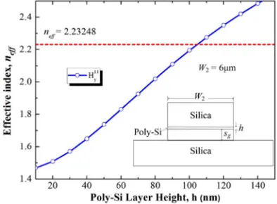
m, 1.4552 and 1.45, respectively. In order to explain the mechanism, the multi-layer based SSCs with one, two and eleven layers are se-quentially simulated by using the rigorousH-field based VFEM and the LSBR method. In each case, the heightðhÞand separation ðSÞneed to be adjusted to achieve the phase matching be-tween the upper and lower waveguides.At first, the analysis for a single Poly-Si layer based SSC is considered. Effective indexðneffÞ
for the fundamental quasi-TE H11y mode of the NW is accurately calculated as being neff¼
2:23248 and shown by a horizontal dashed red line in Fig. 2. A single layer of wider Poly-Si can be phase matched to silicon NW by varying its heighth. Here, its width is taken as 6
m to ex-pand its spot-size horizontally. Variation ofneff with the height of the Poly-Si layerh for the H11ymode is shown in Fig. 2 by a solid blue line. It can be noted that as the heighth of the Poly-Si layer is increased, the neff of the H11y mode is increased and at the crossing point, when
[image:6.594.215.380.62.346.2]h¼107 nm, has the same effective index as that of the silicon NW. Although the phase match-ing condition is shown, when these two guides are isolated, however, the phase matchmatch-ing con-dition for coupled guides also needs to be studied. To identify phase matching between two nonidentical waveguides, it is essential to solve for the supermodes as the phase matching
conditions may differ considerably from the solutions of two isolated waveguides, due to the un-equal loading of each waveguide by the other.
To achieve phase matching for the nonidentical structure, variations of the propagation con-stantsðÞshould be calculated with the separationðSÞand height ðhÞto identify the necessary height for a given separation. The VFEM is used to find the supermodes of the coupled struc-tures consisting two nonidentical waveguides. Variations of the propagation constants for even and odd supermodes with the height of the Poly-Si layer for two different separations, S are shown in Fig. 3(a). When the separation is large, forS¼500 nm, the first supermode, which is even or even-like, is shown by a green dotted line. Its second supermode, which is odd or odd-like is shown by a red dash-dotted line. When the Poly-Si layer height h107 nm, these two propagation constants become closer. The horizontal line sections of these two curves repre-sent the propagation constants of the H11y mode in the lower silicon NW (almost constant), while the slanted line sections of these two curves represent the propagation constants of the
[image:7.594.198.395.60.205.2]H11y mode in the upper Poly-Si layer which is increasing as the h is increased. However, these two curves do not cross each other and both supermodes go through a transformation around this anti-crossing region. Near the phase matching condition, two propagation constants are close to each other and the phase difference between these modes will be smallest. In this sit-uation, two modes become degenerate, get mixed up and formed two supermodes. Especially, curves for S¼500 nm are closer than those for S¼300 nm, which could indicate the curves
[image:7.594.117.478.263.407.2]Fig. 3. Coupling characteristics of a one-layer-based SSC. (a) Even and odd supermode varia-tions with Poly-Si heighthforS¼300 and 500 nm, respectively. (b) Semi-log plot of the variation of coupling lengthLcwithhforS¼300 and 500 nm, respectively.
Fig. 2. Variations ofneff with the height of the Poly-Si layerhfor theH11y mode. The horizontal line
of propagation constants become closer for larger separation between upper and lower wave-guides due to weaker interactions. It can be noted, for S¼300 nm, the difference between two curves of propagation constants become larger due to the strong coupling. In this case, the phase matchinghmoves fromh¼107 nm for isolated or weakly coupled guides toh¼120 nm, which is due to the strong coupling.
The coupling length can be defined asLc ¼=ðevenoddÞ[29] whereevenandoddare the
propagation constants of the even and odd supermodes, respectively. Variations of coupling length with the heightðhÞof the Poly-Si layer are shown in Fig. 3(b) forS¼300 and 500 nm, re-spectively. It can be observed that, when phase matching was achieved, the difference between the propagation constants of the two supermodes was smallest and the coupling length shows a peak value. As separation ðSÞ increases, the peak value of theLc gets larger due to weaker
coupling near the phase matching region. Especially, for a smaller separation, it not only yields a smaller coupling length, but also less sensitive to the variation of the height of the Poly-Si layer, which makes it less sensitive to the fabrication tolerances. For the separationS¼300 nm at the phase matching condition, the coupling length and the SSC length should be 5.5
m.As shown in Fig. 1, an input NW in the Section 1 is butt-coupled to the start of the Section 2 containing the SSC section, identified as z¼0. Transfer of butt-coupled power at this junction to the lower NW of a coupled SSC section is calculated by using the LSBR method from the ex-cited supermodes’ coefficients in the directional coupler section. After propagating along the Section 2, the optical power can be evanescently coupled from the lower silicon NW to the up-per Poly-Si array atz ¼Lc. The transfer of optical power from the lower primary silicon NW, a,
to the upper secondary Poly-Si layer,b, by evanescent coupling at exactlyz ¼Lc may be
calcu-lated from the modal coefficients of two supermodes and their field profiles. For the nonidentical waveguides, most of the traditional coupled mode methods may be inadequate to calculate ac-curately the power transfer between two strongly coupled nonidentical waveguides due to the coefficients of two supermodes will be highly unequal when the guides are not phase matched. The LSBR method has been proved to be an accurate and efficient approach for these type of structures, which is used here to calculate the power transfer efficiency by imposing the continu-ity of the tangentialEandHfields at the junction.
The variations of the normalized power transfer efficiency withh forS¼300 nm are shown in Fig. 4, in whichPaandPb are the power remaining in the silicon NW and the power coupled to
the Poly-Si layer at z ¼Lc, respectively. It can be observed that the maximum power transfer
could be achieved when the heightðhÞof the Poly-Si layer is 118 nm, and the waveguides are phase matched and in this case the power transfer efficiency is 93.2%. It can also be noted that the output power remains within 1 dB of its maximum value when the height,hremains between 114 to 124 nm. The field profile at the end of the SSC sectionðz ¼LcÞis shown as an inset in
[image:8.594.200.394.56.206.2]Fig. 4, which indicates that the field profile has been expanded horizontally by using the SSC. In
this case, the effective areaðAeffÞ[30] of the upper waveguide core is 5.168
m2, which is morethan 12.8 times larger than that of the lower silicon NW. Subsequently, the LSBR method is used again to calculate the coupling efficiency between the SSC and a standard SMF. Since the spot-size has been expanded at the end of the SSC, the coupling efficiency at this junction increased to 21.6% when a single layer wider SSC is considered, compared to only 3.9% for the direct coupling. The total coupling loss is 6.961 dB considering the coupling efficiency of two separate values (93.2% and 21.6%). Meanwhile, power reflection for the single layer based SSC-SMF is reduced to 9.4% compared to the original 30% for the direct butt-coupling of NW to a standard SMF.
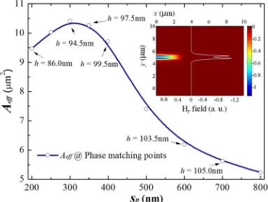
Following this, design of a two-layer based SSC is considered to reduce the coupling loss fur-ther. For two-layer based SSC, the effective area of the two isolated layers also needs to be studied to identify the optimum inner separation. The effective areas are calculated at the phase matching points for different inner separations. Variation of the effective area,Aeff, with the inner
separation,Sp, of two Poly-Si layers is shown in Fig. 5. It can be noted that, for Sp¼300 nm
andh¼94:5 nm, the maximum Aeff of 10.4
m2for the isolated 2-layers can be achieved, andin this case the field profile of the isolated 2-layers Poly-Si is shown as the inset in Fig. 5, pro-viding the maximum spot-size for coupling with the fiber.
Although the poly-Si layer thickness necessary for phase matching of isolated waveguides have been determined, but as the thickness necessary would change slightly when these iso-lated waveguides form a strongly coupled directional coupler with the NW. Next, for the com-bined coupled structure with fixedSp ¼300 nm, the variations of the propagation constants for
even and odd supermodes with the height of the Poly-Si layer are shown in Fig. 6(a). Variations of the propagation constants for even and odd supermodes are calculated with the separation
ðSÞ of 500 and 800 nm, respectively. Variations of coupling length with the height ðhÞ of the Poly-Si layer are shown in Fig. 6(b) for S¼500 and 800 nm, respectively. It can be observed that, when the separationS¼500 and 800 nm, the necessary phase matching can be achieved with the height, h¼96:0 and 95.4 nm, respectively, and these values are different from the heighth¼94:5 nm required for two isolated waveguides for phase matching. For the separation
S¼500 nm, at phase matching the coupling length and the SSC length needs to be 61
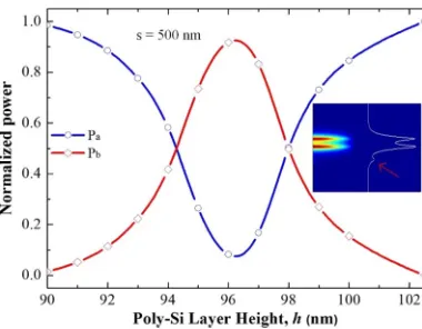
m. Next, transfer of optical power from the input NW to the lower silicon NW in the SSC section atz ¼0 and from the lower silicon NW to the upper two Poly-Si layers atz ¼Lc are calculated [image:9.594.201.393.60.205.2]by using the LSBR method. The modal coefficients can be calculated by using the LSBR method and from these modal coefficients and modal field profiles of the supermodes, obtained by the FEM, the power transfer efficiency could be calculated. The variations of the normalized power transfer efficiency withh forS¼500 nm are shown in Fig. 7, in whichPaandPb are the
Fig. 5. Variations of effective areaAeff with the separation between the Poly-Si layersSpat
power remaining in the silicon NW and the power coupled to the two Poly-Si layers atz ¼Lc,
re-spectively. It can be observed that the maximum power transfer could be achieved when the heightðhÞof the Poly-Si layer is 96 nm, in which the power transfer efficiency is 91.8%. It can be also noted that the output power remains within 1 dB of its maximum value when the height,
h remains between 95.2 to 97.2 nm. The field profile at the end of the SSC sectionðz ¼LcÞis
shown as an inset in Fig. 7, which demonstrate that the field profile has been expanded by using the SSC. A small kink below the two-layer, shown by a red arrow, indicates a small amount of field remained in the lower NW. In this case, theAeff of the upper waveguide core is
10.41
m2, which is more than 26 times larger than that of the lower silicon NW. The LSBR method is used again to calculate the coupling efficiency between the SSC and a standard SMF. Since the spot-size has been expanded at the end of the SSC, the coupling efficiency at this junction increased from 3.9% for the direct coupling to 27.0% when a two-layer based SSC is considered. The total coupling loss is 6.06 dB considering the coupling efficiency at two sepa-rate junctions (91.8% and 27.0%) and reflected power at the end of the two-layer based SSC-SMF interface is 8.9%. [image:10.594.118.480.56.202.2]To increase the spot-size further in the vertical direction, design of an eleven-layer based SSC is considered. To achieve phase matching for 11 isolated waveguides, it is necessary to calculate the variations of the effective indices of the upper waveguide neff with the height
Fig. 6. Coupling characteristics of a two-layer-based SSC. (a) Even- and odd-like supermode vari-ations with Poly-Si heighthforS¼500 and 800 nm, respectively. (b) Semi-log plot of the variation of coupling lengthLcwithhforS¼500 and 800 nm, respectively.
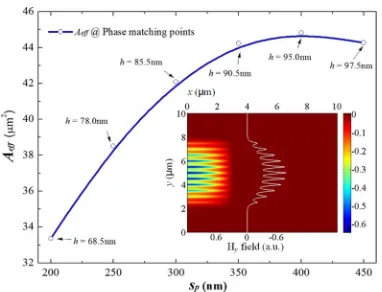
[image:10.594.202.392.272.420.2]ðhÞ and inner separation ðSpÞ to identify the necessary inner separation. Variations of the
ef-fective area Aeff with inner separation Sp of 11 Poly-Si layers are shown in Fig. 8. The
effec-tive areas are calculated at phase matching points for different inner separations. It can be noted that forSp ¼400 nm andh¼95:0 nm, the maximum Aeffof 44.8
m2for the isolated 11 layerscan be achieved, and in that case, the field profile of the isolated Poly-Si 11-layers is shown as the inset in Fig. 8, providing the maximum spot-size for coupling with the fiber.
Next, for the combined coupled structure fixedSp¼400 nm, the variations of the propagation
[image:11.594.203.394.57.203.2]constants for even and odd supermodes with the height of the Poly-Si layer are shown in Fig. 9(a). The propagation constants for even and odd supermodes are calculated with the separationðSÞof 200 and 500 nm, respectively. Then, the variations of coupling length with the height ðhÞof the Poly-Si layer are shown in Fig. 9(b) forS¼200 and 500 nm, respectively. It can be observed that, when the separationS¼200 and 500 nm, the necessary phase matching can be achieved with the height h¼105 and 87.2 nm, respectively. When a coupled structure is composed of eleven identical waveguides, they are always phase matched when the separation between them changes. However, for nonidentical waveguides, the phase matching also depends on mutual load-ing of the waveguides, in which their phase matchload-ing condition can be altered significantly due to unequal loading of each other. Therefore, the phase matching condition for height value changes with S shown here, which is also different from the height for phase matching of the 11 isolated
Fig. 8. Variations of effective areaAeff with the separation between the Poly-Si layersSpfor the even modes at phase-matching points for 11 Poly-Si layers. (Inset) Modal field profile of the iso-lated layers for maximumAeff.
[image:11.594.117.478.271.415.2]waveguides. For the separationS¼200 nm, at phase matching the coupling length and the SSC length needs to be 158.67
m.Next, transfer of optical power from the input NW to the lower silicon NW of the SSC atz¼0 and from the lower silicon NW to the upper 11 Poly-Si layers at exactlyz ¼Lc are calculated by
using the LSBR method. The modal coefficients can be obtained from these modal coefficients and modal field profiles of the supermodes by using the LSBR method. Following that, the power transfer efficiency can be calculated with these modal coefficients and modal field profiles of the supermodes. As shown in Fig. 10, the variations of the normalized power transfer effi-ciency are with h for S¼200 nm, in which Pa and Pb are the powers remaining in the silicon
NW and coupled to the 11 Poly-Si layers at z¼Lc, respectively. The maximum 95.2% power
transfer could be achieved when the heightðhÞof the Poly-Si layer is 105 nm. It can be noted that the output power remains within 1 dB of its maximum value when the height,hremains be-tween 103 to 121.5 nm. The field profile at the end of the SSC sectionðz¼LcÞis shown as an
inset in Fig. 10, which can indicate that the field profile has been expanded significantly by using the SSC. In this case, theAeff of the upper waveguide core is 44.5
m2, which is more than twoorders larger than that of the lower silicon NW. The LSBR method is used again to calculate the coupling efficiency between the SSC and the SMF. Since the spot-size has been expanded at the end of the SSC, the coupling efficiency at this junction will increase from 3.9% for the direct coupling to 56.1% when an eleven-layer wider SSC is considered. The total coupling loss is only 2.72 dB considered the coupling efficiency of two separate values (95.2% and 56.1%) at two junctions and the 11 layer based SSC-SMF power reflection is 6.8%. However, instead of a standard SMF, if a smaller lensed fiber can be introduced to couple with the multi-layer based SSC, a higher coupling efficiency can be achieved. For the same normalized frequency, V, as for a standard SMF, the radius of a lensed fiber is taken as 2
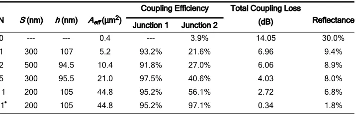
m as an example and the core and cladding refractive indices are taken as 1.4731 and 1.45, respectively. The coupling effi-ciency between the 11 layer based SSC and the lensed fiber can be dramatically improved to 97.1%, and the total coupling loss is reduced to only 0.34 dB. The reflected power at the end of the 11-layer based SSC-SMF interface is reduced to only 1.8%. [image:12.594.198.393.56.208.2]To give the coupling performance for different Poly-Si layers, the SSC with one, two, five and eleven Ploy-Si layers are calculated, which are summarized in Table 1. It can be noted that the coupling efficiency of the Junction 1 is the power transfer from the silicon NW to the multi-Poly-Si layers, while the Junction 2 is the coupling between the SSC and the standard SMF. The total coupling loss is the sum of the coupling losses of the Junctions I and II. It can be observed from Table 1 that the effective area is increased with the increase of the layer number, and therefore, larger spot-size could be achieved with more layers. Therefore, the total coupling loss can be significantly reduced from 14.05 dB to 2.72 dB by using an 11 layer based SSC. It can also be
observed that the 11 layer based SSC-SMF power reflection is reduced to 6.8% compared to the original 30% for the direct silicon NW and SMF coupling. It should be noted that, when a sili-con NW is directly butt-coupled to a standard SMF, the reflection is due to both mode-size mis-match and impedance mismis-match. On the other hand, when this multi-layer based SSC is butt-coupled to the standard SMF, the mode size mismatch is reduced but remaining impedance mismatch is responsible for the reflection, although much smaller. The SSC facet could be anti-reflection coated for a further reduction in the overall power anti-reflection.
Recently, the use of an inverted taper obtained by the reduction of the width of the sili-con nanowire with a fiber-adapted polymer waveguide, yield a coupling loss of ∼0.66 dB and∼0.36 dB between the inverted taper and the tapered fiber with 2.9-
m mode-size diameter for the TE and TM polarizations, respectively [31]. However, such structure requires a taper tip width smaller than 15 nm for a smaller than 250-nm-thick silicon layer, which is not trivial to fabri-cate by using the standard CMOS process.4. Conclusion
In conclusion, we have proposed a novel concept and designed and optimized the nanopho-tonic coupling using a multi-layer based SSC, which is composed of non-tapered structure. This compact structure can be fabricated by using the CMOS process and be directly integrated. An efficient algorithm, combining the VFEM and the LSBR, has been developed to find the mode profiles and power transfer efficiency for the SSC. Here, the single and multi-Poly-Si layers based SSCs are investigated, in which the coupling process, phase matching for isolated and combined waveguides are given. With an 11 Poly-Si layers based SSC, the coupling loss be-tween the silicon NW and the SMF can be reduced to 2.72 dB. On the other hand, instead of a standard SMF, a lensed fiber of radius 2
m is used, the coupling loss is considerably re-duced to 0.34 dB. However, if desired, the coupling loss can be further rere-duced by using more layers and using the Poly-Si layer of larger width, which can be incorporated in the PIC system on chip.References
[1] H. Subbaramanet al.,“Recent advances in silicon-based passive and active optical interconnects,”Opt. Exp., vol. 23, no. 3, pp. 2487–2511, 2015.
[2] B. Jalali and S. Fathpour,“Silicon photonics,”J. Lightw. Technol., vol. 24, no. 12, pp. 4600–4615, 2006.
[3] P. P. Absilet al.,“Silicon photonics integrated circuits: A manufacturing platform for high density, low power optical I/O’s,”Opt. Exp., vol. 23, no. 7, pp. 9369–9378, 2015.
[4] D. Liang and J. E. Bowers,“Recent progress in lasers on silicon,”Nature Photon., vol. 4, no. 8, pp. 511–517, 2010. [5] G. T. Reed, G. Mashanovich, F. Y. Gardes, and D. J. Thomson,“Silicon optical modulators,”Nature Photon., vol. 4,
[image:13.594.121.479.91.206.2]no. 8, pp. 518–526, 2010.
[6] C. Koppet al.,“Silicon photonic circuits: On-CMOS integration, fiber optical coupling, and packaging,”IEEE J. Sel. Top. Quantum Electron., vol. 17, no. 3, pp. 498–509, May/Jun. 2011.
[7] H. Ronget al.,“A continuous-wave Raman silicon laser,”Nature, vol. 433, no. 7027, pp. 725–728, 2005.
[8] D. Marris-Morini, L. Vivien, J. M. Fédéli, E. Cassan, P. Lyan, and S. Laval,“Low loss and high speed silicon optical modulator based on a lateral carrier depletion structure,”Opt. Exp., vol. 16, no. 1, pp. 334–339, 2008.
[9] A. Liu et al., “A high-speed silicon optical modulator based on a metal-oxide-semiconductor capacitor,” Nature, vol. 427, no. 6975, pp. 615–618, 2004.
[10] G. Roelkenset al.,“III-V/silicon photonics for on-chip and intra-chip optical interconnects,”Laser Photon. Rev., vol. 4, no. 6, pp. 751–779, 2010.
[11] J. S. Levy, A. Gondarenko, M. A. Foster, A. C. Turner-Foster, A. L. Gaeta, and M. Lipson,“CMOS-compatible multiple-wavelength oscillator for on-chip optical interconnects,”Nature Photon., vol. 4, no. 1, pp. 37–40, 2010.
[12] F. E. Doanyet al.,“Multichannel high-bandwidth coupling of ultradense silicon photonic waveguide array to standard-pitch fiber array,”J. Lightw. Technol., vol. 29, no. 4, pp. 475–482, 2011.
[13] G. Masanovicet al.,“A high efficiency input/output coupler for small silicon photonic devices,”Opt. Exp., vol. 13, no. 19, pp. 7374–7379, 2005.
[14] G. Roelkenset al.,“High efficiency diffractive grating couplers for interfacing a single mode optical fiber with a nano-photonic silicon-on-insulator waveguide circuit,”Appl. Phys. Lett., vol. 92, no. 13, 2008, Art. no. 131101.
[15] H. L. Tseng, E. Chen, H. Rong, and N. Na,“High-performance silicon-on-insulator grating coupler with completely vertical emission,”Opt. Exp., vol. 23, no. 19, pp. 24 433–24 439, 2015.
[16] A. Bozzola, L. Carroll, D. Gerace, I. Cristiani, and L. C. Andreani,“Optimising apodized grating couplers in a pure SOI platform to−0.5 dB coupling efficiency,”Opt. Exp., vol. 23, no. 12, pp. 16 289–16 304, 2015.
[17] C. Li, K. S. Chee, J. Tao, H. Zhang, M. Yu, and G. Q. Lo,“Silicon photonics packaging with lateral fiber coupling to apodized grating coupler embedded circuit,”Opt. Exp., vol. 22, no. 20, pp. 24 235–24 240, 2014.
[18] T. H. Lohet al.,“Ultra-compact multilayer Si/SiO2GRIN lens mode-size converter for coupling single-mode fiber to Si-wire waveguide,”Opt. Exp., vol. 18, no. 21, pp. 21519–21533, 2010.
[19] H. Yoda and K. Shiraishi,“A new scheme of a lensed fiber employing a wedge-shaped graded-index fiber tip for the coupling between high-power laser diodes and single-mode fibers,”J. Lightw. Technol., vol. 19, no. 12, p. 1910, 2001.
[20] L. Jiaet al.,“Analysis of the polarization rotation effect in the inversely tapered spot size converter,”Opt. Exp., vol. 23, no. 21, pp. 27 776–27 785, 2015.
[21] Q. Wanget al.,“Heterogeneous Si/III-V integration and the optical vertical interconnect access,”Opt. Exp., vol. 20, no. 15, pp. 16745–16756, 2012.
[22] J. Zou et al.,“Short and efficient mode-size converter designed by segmented-stepwise method,”Opt. Lett., vol. 39, no. 21, pp. 6273–6276, 2014.
[23] X. Sun, L. Zhou, H. Zhu, Q. Wu, X. Li, and J. Chen,“Design and analysis of a miniature intensity modulator based on a silicon-polymer-metal hybrid plasmonic waveguide,”IEEE Photon. J., vol. 6, no. 3, pp. 1–10, Jun. 2014. [24] J. Puet al.,“Heterogeneous integrated III-V laser on thin SOI with single-stage adiabatic coupler: Device realization
and performance analysis,”IEEE J. Sel. Topics Quantum Electron., vol. 21, no. 6, Nov./Dec. 2015, Art. no. 1501808. [25] B. M. A. Rahman and J. B. Davies,“Finite-element solution of integrated optical waveguides,”J. Lightw. Technol.,
vol. 2, no. 5, pp. 682–688, 1984.
[26] M. Rajarajan, B. M. A. Rahman, T. Wongcharoen, and K. T. V. Grattan,“Accurate analysis of MMI devices with two-dimensional confinement,”J. Lightw. Technol., vol. 14, no. 9, pp. 2078–2084, 1996.
[27] T. Wongcharoen, B. M. A. Rahman, and K. T. V. Grattan, “Accurate characterization of optical filters with two-dimensional confinement,” J. Lightw. Technol., vol. 14, no. 11, pp. 2596–2603, 1996.
[28] B. M. A. Rahman and J. B. Davies,“Analysis of optical waveguide discontinuities,”J. Lightw. Technol., vol. 6, no. 1, pp. 52–57, 1988.
[29] A. Barh, B. M. A. Rahman, R. K. Varshney, and B. P. Pal,“Design and performance study of a compact SOI polari-zation rotator at 1.55m,”J. Lightw. Technol., vol. 31, no. 23, pp. 3687–3693, 2013.
[30] D. M. H. Leung, N. Kejalakshmy, B. M. A. Rahman, and K. T. V. Grattan,“Rigorous modal analysis of silicon strip nanoscale waveguides,”Opt. Exp., vol. 18, no. 8, pp. 8528–8539, 2010.