Dislocation-mediated plasticity in silicon during nanometric cutting:
A molecular dynamics simulation study
Saeed Zare Chavoshi
a, Shuozhi Xu
b, Xichun Luo
a,n aCentre for Precision Manufacturing, Department of Design, Manufacture and Engineering Management, University of Strathclyde, Glasgow G1 1XJ, UK
bGWW School of Mechanical Engineering, Georgia Institute of Technology, Atlanta, GA 30332-0405, USA
a r t i c l e i n f o
Article history:
Received 25 February 2016 Received in revised form 4 May 2016
Accepted 6 May 2016 Available online 19 May 2016
Keywords:
Molecular dynamics Dislocation nucleation Amorphization Nanometric cutting Single crystalline silicon
a b s t r a c t
The nucleation and propagation of dislocations and its consequence on the defect structure in silicon during nanometric cutting are not well known, although the amorphization and high pressure phase transformation studies on silicon have remained at the epicentre of research across various disparate disciplines for over a decade. This paper proposes a new mechanism of crystal plasticity identified by a fully automated dislocation extraction algorithm in molecular dynamics simulations of nanometric cutting of silicon for different cutting planes/directions at a wide range of temperatures (300–1500 K). Alongside amorphization of silicon, our simulations revealed nanoscale stochastic nucleation of dis-locations and stacking faults, which serve as mediators of microscopic plasticity during various contact loading operations and manufacturing processes of silicon. Of interest is that, irrespective of the cutting temperature, the stacking faults, which were not formed for either the (010)[100] or (111)[11̅ 0] crystal setups, were generated with three atomic layers in the (110)[001̅] cutting.
&2016 The Authors. Published by Elsevier Ltd. This is an open access article under the CC BY license (http://creativecommons.org/licenses/by/4.0/).
1. Introduction
Silicon, a diamond cubic lattice structured material, exhibits strong and directionalsp3bonding and has two sets of {111} slip
planes, the shuffle and the glide sets. Recent molecular dynamics (MD) simulation studies of high-power, pulsed, laser-driven shock compression of silicon revealed that partial dislocations and stacking faults can be emitted from the surface under pressures that are slightly higher than 10 GPa[1,2]. Likewise, in MD simu-lations of strained silicon nanowires of different lengths, the yield was exhibited by dislocation nucleation[3,4]. Nevertheless, pre-vious studies in nanometric cutting of silicon showed that the ductility and plasticity of silicon are direct consequences of amorphization rather than dislocation nucleation and migration [5,6].
A key question thus is whether the nucleation and migration of dislocations and other crystal defects assist in crystal plasticity of silicon during nanometric cutting at room and high temperatures. Previous MD studies failed to answer this question primarily due to the application of an improper interatomic potential function, i.e. Tersoff[7], to describe the dislocation cores[8]. Accordingly, the present study aims to gain an in-depth understanding of the plasticity mechanisms of silicon during nanometric cutting at
different temperatures, using the Stillinger-Weber (SW) potential function[9]with the aid of the dislocation extraction algorithm (DXA)[10]. The DXA has a proven ability to identify dislocations in diamond structure such as Si[5]and Ge[11]; its algorithm is based on a discrete Burgers circuit integral over the elastic displacement field and is not limited to specific lattices or dislocation types[10]. The virtual X-ray diffraction (XRD)[12]analysis is also carried out to quantify the structural changes of silicon.
2. Computational method
The three-dimensional MD model of nanometric cutting is il-lustrated inFig. 1, with the details of simulation model and process parameters summarized inTable 1. The simulation methodology is the same as in our previous work[13–15], i.e. the region of atoms in the tool and the substrate were divided into three zones namely, boundary atom zone, thermostatic atom zone and Newtonian atom zone. The boundary atoms were held rigid to reduce the boundary effects and to maintain the symmetry of the lattice. The Newtonian region followed the Newtonian dynamics (NVE en-semble) while the thermostat zone was updated according to the Berendsen thermostat to emulate the effect of heat carriers like chips and lubricants. The periodic boundary conditions (PBCs) were imposed along thezdirection of the simulation domain to reduce the effects of simulation scale. The MD simulations were conducted using LAMMPS[16]with an“Open Visualization Tool” Contents lists available atScienceDirect
journal homepage:www.elsevier.com/locate/mssp
Materials Science in Semiconductor Processing
http://dx.doi.org/10.1016/j.mssp.2016.05.003
1369-8001/&2016 The Authors. Published by Elsevier Ltd. This is an open access article under the CC BY license (http://creativecommons.org/licenses/by/4.0/).
nCorresponding author.
(OVITO) [17] and DXA [10] to visualise and analyse the atomic trajectories.
The SW potential function [9], which incorporates a linear combination of two- and three-body terms, was employed to de-scribe the interactions between silicon atoms (Si-Si) in the sub-strate whereas an analytical bond order potential (ABOP) formal-ism[18]was adopted to dictate the interactions between diamond atoms (C-C) in the cutting tool as well as those between substrate and tool atoms (Si-C). The SW potential provides a better ap-proximation of the maximum restoring force, the theoretical shear strength, and the strain associated with the critical stress for both shuffle and glide sets planes than the Tersoff[7]and Environment-Dependent Interatomic Potential[19]potentials. Moreover, the SW potential leads to smooth stacking fault energy (SFE) variations, in agreement with ab-initiosimulations [8,20,21]. Some caveats of the SW potential include an underestimation of the unstable/ stable SFE for the shuffle set-plane and an overestimation of them for the glide set-plane. As a result, it is expected that for the glide set-plane, using the SW potential, (1) both the leading and trailing partials are more difficult to nucleate and (2) the stacking fault width is smaller, compared withab-initiosimulations. The oppo-site is true for the shuffle set-plane. Nevertheless, in the motion of dislocations, the unstable SFE is less important than the rebound force of the lattice subject to large deformations, which is accu-rately given by the SW potential[8]. The SW potential also accu-rately reproduces the melting temperature of silicon which,
however, comes as a price that the cohesive energy is rescaled; by consequence, the elastic constants are also rescaled, leading to some inconsistencies in reproducing relevant mechanical proper-ties of silicon with those of experiments, as indicated inAppendix A. Taking into account the restricted transferability of empirical potentials, the SW potential is a good choice for exploring dis-location-mediated plasticity of silicon at room and elevated tem-peratures during nanometric cutting.
In order to obtain accurate simulation results, wefirst calcu-lated the cohesive energies and corresponding equilibrium lattice constants of silicon at various temperatures using the SW potential energy function, as shown inTable 2; these lattice constants are subsequently utilized to build the geometry of the substrate. In all cases, the tool was equilibrated at 300 K; hence the lattice con-stant of 3.568 Å calculated using the ABOP function at 300 K was used for the carbon atoms. Note that the cohesive energy was time-averaged over 1 ns under NPT ensemble.
3. Results and discussion
[image:2.595.141.466.56.252.2]Nanometric cutting involves plastic deformation of materials at high strain rates. The slip systems with the largest resolved shear stress along the Burgers vector are activated on the threshold of plasticity. Dislocation glide in silicon occurs in two widely and narrowly spaced {111} dense planes, shuffle and glide sets, re-spectively[8]. However, at high temperatures slip can also take place in the {110} and {100} planes[24].
[image:2.595.41.294.313.453.2]Fig. 1.Schematic diagram of the MD simulation model of nanometric cutting. Different cutting planes (yplane) and cutting directions (xdirection) are tested at a wide range of temperatures.
Table 1
Details of the MD simulation model and the cutting parameters used in the study.
Substrate/tool material Single crystalline silicon/diamond
Substrate dimensions 381910.8 nm3
Cutting edge radius (tip radius) 3.5 nm Uncut chip thickness (cutting depth in 2D) 3 nm Cutting plane (yplane) and cutting
direc-tion (xdirection)
Case 1: (010)[100] Case 2: (110)[001]̅ Case 3: (111)[110]̅ Rake and clearance angle of the cutting
tool
25°and 10°
Substrate temperature 300 K, 750 K, 850 K, 1173 K, 1273 K, 1500 K
Cutting speed 50 m/s
Time step 1 fs
Potential energy function SW[9]
Table 2
Calculated equilibrium lattice constants and cohesive energies of silicon at different temperatures using SW potential energy function. The cohesive energy calculated here is slightly lower than the experimental value of4.6270.08 eV[22], which potentially results in smaller elastic constants. We assume that such effects are small in the context of this work, which focuses on the plastic response of silicon.
Temperature (K) lattice con-stant (Å)
cohesive en-ergy (eV)
Experimental lattice con-stant (Å)[23]
300 5.4348 4.3355 5.431
750 5.4405 4.3338 5.439
850 5.4423 4.3326 –
1173 5.4458 4.332 5.449
1273 5.4473 4.3312 5.452
1500 5.4502 4.3308 5.457
[image:2.595.311.563.660.744.2]3.1. Case 1: (010)[100] cutting
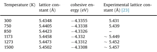
Figs. 2and3show the formation of defects during nanometric cutting of silicon on the (010) crystal plane at two cutting dis-tances (10 nm and 20 nm) and two typical temperatures (300 K and 1500 K). The white atoms demonstrated in thesefigures sig-nify the highly-disordered (amorphous) atoms, obtained via monitoring the local environment of atoms up to the second neighbor shell using the diamond structure identification tool in OVITO[11]. It is shown that the cutting chip and subsurface re-spond by local amorphization followed by dislocation formation and migration near the cutting sites. Further characterization of the crystal qualities of silicon atoms was performed by virtual XRD
[12], as detailed in Appendix B. As evident inFig. 2(a), a perfect 60° dislocation with 1[101̅ ]
2 Burgers vector glides ahead of the cutting tool, which facilitates the crystal plasticity of silicon during na-nometric cutting at room temperature. At a larger cutting distance of 20 nm, more perfect 60°dislocations are nucleated within the substrate. Of interest is the dissociation of one perfect screw dis-location with 12[ ̅101] Burgers vector into two partials, i. e. a
Shockley partial with 1[121̅ ]
6 Burgers vector and another partial with 1[ ̅211]
[image:3.595.129.457.182.717.2]3 Burgers vector, possibly due to the high local stress immediately ahead of the cutting tool. This agrees with a recent finding that an undissociated perfect dislocation in the shuffle-set plane can switch to the glide-set plane and dissociate subject to a
large shear stress[8].
At 1500 K and a short cutting distance of 10 nm, a perfect 60° dislocation with 1[011̅ ]
2 Burgers vector is nucleated underneath the cutting tool. However, this dislocation stopped after migrating for a short distance, suggesting that it only slightly assists in the plasticity of silicon. Note that, generally, dislocations ahead of the tool tip moving the crystalline region play a more important in plasticity during the nanometric cutting process because they drive the plasticity and promote the ductility more than those located beneath and behind the cutting tool. Should the disloca-tion activities be subdued, the plasticity is primarily driven by amorphization and weaker bonding between atoms at high tem-peratures. With the increase of temperature, the amplitude of atomic vibration within the substrate increases, as well as the
number of phonons. The increased atomic displacements within the substrate lead to a rise in the averaged interatomic distances, which lowers the energy needed to break the atomic bonds and facilitates the thermal softening and amorphization. Note that an increase of dislocation density at higher temperatures was not observed in our simulations, as opposed to what was observed for the cubic silicon carbide[15]. The total length of dislocations was found to vary haphazardly from 11.4 nm to 14.4 nm and from 40.1 nm to 60 nm at the short and long cutting distances, re-spectively, over the studied temperatures.
3.2. Case 2: (110)[001̅] cutting
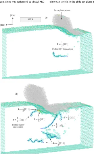
As seen in Fig. 4, while cutting the (110) surface at 300 K, perfect 60°dislocations with 1[110̅ ]
[image:4.595.138.467.242.548.2]2 Burgers vector are nucleated Fig. 3.Dislocation nucleation while cutting the (010) plane at 1500 K at a cutting distance of (a) 10 nm and (b) 20 nm.
ahead of the cutting tool. As the cutting process advances, perfect 60°dislocations are nucleated continuously, as shown inFig. 4(b), in accordance with the results for the (010) plane.
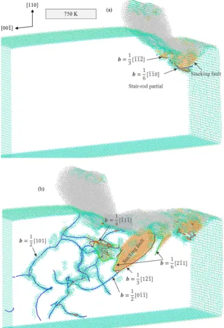
Fig. 5(a) shows that at 750 K, stair-rod partials with 1[ ̅ ̅ ]1 10 6 Burgers vectors emerged. In addition, a quadric shape-stacking fault bounded between partial dislocations, in accordance with the experimental observation [24]. Note that the partial dislocations do not arise from dissociation of perfect dislocations, but are nu-cleated independently; the dislocation-originated stacking fault consists of three atomic layers. It is thus demonstrated that plane defects, such as the stacking faults, can be formed within the confined volume of silicon substrate. It is observed from Fig. 5 (b) that numerous perfect 60° dislocations, partials and a large stacking fault, bounded between a Shockley partial with 16[211̅ ]
Burgers vector and another partial with13[121̅ ̅ ]Burgers vector, are formed at the cutting distance of 20 nm. Previous MD simulations
showed that under high temperature and low stress conditions, dislocations are more likely nucleated in the glide-set plane over the shuffle-set plane [25,26]. Li and Picu [8] reported that a pressure increase leads to a reduction in the activation energy for nucleation in the shuffle-set, confirming that dislocations tend to be nucleated in the shuffle-set at high stress levels, e. g. in the regions beneath the cutting tool.
It is worth mentioning that while cutting the (110) at 850 K, at short cutting distances, no stacking faults were observed as op-posed to the 750 K case. At higher temperatures of 1173 K and 1273 K, three atomic layers-stacking fault bounded between par-tials was formed underneath the cutting tool. Moreover, the size of the stacking fault increased as the cutting advanced.
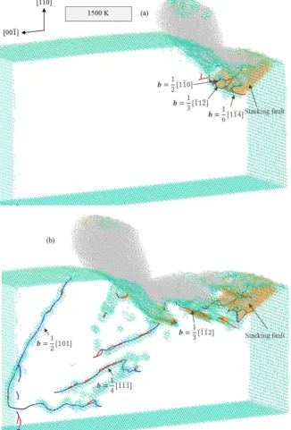
[image:5.595.130.459.61.528.2]Quadric shape-stacking fault, perfect 60°dislocations and par-tial dislocations are formed at 1500 K and a cutting distance of 10 nm, as shown inFig. 6(a). Interestingly, the stacking fault does Fig. 4.Dislocation nucleation while cutting the (110) plane at 300 K at a cutting distance of (a) 10 nm and (b) 20 nm. The two long perfect 60°dislocations with1[ ̅110]
2 and
⎡⎣110̅ ⎤⎦
1
not grow during the cutting. At a cutting distance of 20 nm, perfect 60°dislocations and partials are nucleated ahead of the cutting tool; partial dislocations, which are on the glide-set planes, are more prevalent at high temperatures, in agreement with the ex-periments[27]. Nevertheless, there is no sharp transition between two regimes of dissociated and undissociated dislocations at high temperatures. The total length of dislocations varied randomly from 27.8 nm to 89.6 nm and from 105.6 nm to 258.7 nm at the short and long cutting distances, respectively, over the studied temperatures.
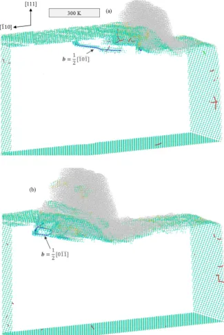
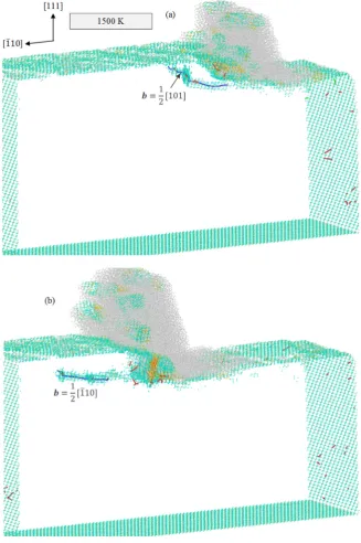
3.3. Case 3: (111)[11̅ 0] cutting
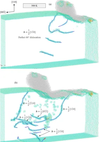
During nanometric cutting of silicon on the (111) crystal plane at different temperatures, mostly perfect 60° dislocations are
nucleated ahead of the cutting tool, as illustrated inFigs. 7and8. The total length of dislocations was found to vary stochastically from 22.1 nm to 48.4 nm and from 24.4 nm to 59.6 nm at the short and long cutting distances, respectively, over the studied tem-peratures. The pattern of dislocation emission is almost identical at different cutting temperatures and distances, i.e. nucleation of perfect 60°dislocations ahead of the cutting tool and near the free surface without stacking faults.
3.4. A comparison between three cases
[image:6.595.138.467.61.541.2]In general, more defects were found for the (110)[001̅] cutting than in the other two cases, which could be attributed to the ease of activating slip systems in this crystal setup. However, a Schmid factor analysis is not suitable due to the complicated stress state in Fig. 5.Formation of crystal defects while cutting the (110) plane at 750 K at a cutting distance of (a) 10 nm and (b) 20 nm. Pink rod represents the stair-rod partial dislocation. (For interpretation of the references to color in thisfigure legend, the reader is referred to the web version of this article.)
adjacent to the cutting tool. Moreover, the dislocation nucleation and stacking fault formation are stochastic at different cutting distances and temperatures in all three cases, with perfect 60° dislocations more prevalent than perfect screw dislocations and partial dislocations.
Our simulations found that for the (010)[100] and (111)[11̅ 0] cutting, dislocation nucleation without stacking faults marginally assists the crystal plasticity of silicon at all temperatures such that the plasticity is mainly controlled by the amorphization and weak bonding between atoms at high temperatures. In contrast, dis-locations and stacking faults dominate the plastic deformation of the silicon substrate in the case of (110)[001̅] cutting at different temperatures, especially at the longer cutting distances. We re-mark that at the initial stage of the (110)[001̅] cutting, the in-cipient plasticity still corresponds to the amorphization of silicon
atoms. This could provide a new insight to understand the brittle-to-ductile transition in silicon.
4. Conclusions
[image:7.595.130.457.63.545.2]during cutting the (110)[001̅] at different temperatures than the (010)[100] and (111)[11̅ 0] crystal setups. Also, perfect 60° location nucleation was more prevalent than perfect screw dis-locations and partial disdis-locations, the latter of which were more likely formed at higher temperatures and in regions of a higher shear stress.
Acknowledgments
SZC would like to thank the help of Dr. Saurav Goel from Queen's University, Belfast, UK for his useful advice. SZC and XL gratefully acknowledge thefinancial support from the EPSRC (EP/ K018345/1) and Royal Society-NSFC International Exchange Pro-gramme (IE141422) for this study, as well as the use of the EPSRC
(EP/K000586/1) funded ARCHIE-WeSt High Performance Compu-ter at the University of Strathclyde. SX acknowledges the Extreme Science and Engineering Discovery Environment (XSEDE), which is supported by National Science Foundation Grant no. ACI-1053575.
Appendix A
[image:8.595.139.465.60.547.2]Study of nanometric cutting at a wide range of temperatures requires an interatomic potential function that correctly predicts the temperature dependence as well as thermal softening. Hence, it is indispensable that the selected potential function reproduces the melting temperature of silicon accurately. To obtain the melting point of silicon estimated by the SW potential, the solid-liquid coexistence method was employed. A 15×15×60lattice Fig. 7. Dislocation nucleation while cutting the (111) plane at 300 K at a cutting distance of (a) 10 nm and (b) 20 nm.
cells comprising of 108000 atoms was equilibrated at an initial guess in a way that the longest direction, [001], was normal to the solid-liquid interface, and the entire simulation was repeated to bracket the melting point. An NPT ensemble was employed at the relaxation step, where only the box length in the zdirection is allowed to change, leading to a seamless, merged solid and liquid system along that direction. The detailed procedure can be found elsewhere[28–29].Fig. A1showed that the simulation cell soli-difies completely at 1670 K after 8.4 ns. Similarly, the simulation cell melts entirely at 1690 K after 5.7 ns. The melting point is de-termined to be Tm=1678K, where the line of average potential energy has an almost zero slope, as demonstrated in Fig. A1. Clearly, there is a good consistency between the experimental value of melting point (1687 K)[30]and that predicted by the SW potential in this study.
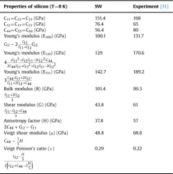
Using the SW potential function, we reproduced the
mechanical properties of silicon, such as elastic constants, bulk modulus, shear modulus, Young's modulus for the three sets of crystallographic directions/planes, and Voigt averages at 0 K, as listed inTable A1. It is found that there exist some inconsistencies between the predicted and experimental values, as a consequence of that the cohesive energy is rescaled to reproduce the accurate melting temperature.
Appendix B
[image:9.595.128.456.61.554.2]spacing parameter of 0.092 between diffraction angles (2
θ
) ranges of 10°to100°on an elemental atomic volume (212 nm3) inthe cutting deformation zone [13]. Virtual 2
θ
x-ray diffraction patterns are demonstrated inFig. B1for the (010)[100] cutting in case 1. Peaks at 2θ
values of 28.41°, 47.3°, 56.12°, 69.17°, 76.37°, 87.16°and 94.91°shown inFig. B1(a) and B1b correspond to the crystalline silicon, which is well-matched with the XRD pattern of standard silicon powder[32]. The strongest reflection, Si (111), at 2θ¼
28.41° corresponds to an interplanar spacing of 3.14 Å. As evident fromFig. B1(b), no shift of the intensity peaks is observed after increasing the temperature of substrate before nanometric cutting, signifying no alteration in the interplanar spacing.Fig. B1 (c) reveals that after cutting at 300 K, the main peaks are dimin-ished remarkably and several new diffractions appear, suggesting that a transformation towards an amorphous configuration has happened for the atoms in the cutting region.References
[1]S. Zhao, et al., Amorphization and nanocrystallization of silicon under shock compression, Acta Mater. 103 (2016) 519–533.
[2]S. Zhao, et al., Pressure and shear-induced amorphization of silicon, Extrem. Mech. Lett. 5 (2015) 74–80.
[3]F.A. El Nabi, et al., Onset of ductility and brittleness in silicon nanowires mediated by dislocation nucleation, Model. Simul. Mater. Sci. Eng. 23 (2) (2015) 025010.
[4]J. Godet, et al., Surface effects on the mechanical behavior of silicon nano-wires: Consequence on the brittle to ductile transition at low scale and low temperature, Phys. Status Solidi A 212 (8) (2015) 1643–1648.
[5]S. Goel, et al., Influence of microstructure on the cutting behaviour of silicon, Acta Mater. 105 (2016) 464–478.
[6]S. Goel, et al., Diamond machining of silicon: a review of advances in mole-cular dynamics simulation, Int. J. Mach. Tools Manuf. 88 (2015) 131–164. [7]J. Tersoff, Modeling solid-state chemistry: Interatomic potentials for
multi-component systems, Phys. Rev. B 39 (1989) 5566.
[8]Z. Li, R.C. Picu, Shuffle-glide dislocation transformation in Si, J. Appl. Phys. 113 (2013) 083519.
[9]F.H. Stillinger, T.A. Weber, Computer simulation of local order in condensed phases of silicon, Phys. Rev. B 31 (8) (1985) 5262–5271.
[10]A. Stukowski, K. Albe, Extracting dislocations and non-dislocation crystal de-fects from atomistic simulation data, Model. Simul. Mater. Sci. Eng. 18 (2010) 085001.
[11] E. Maras, Global transition path search for dislocation formation in Ge on Si (001), Comput. Phys. Com. (2016), in press,http://dx.doi.org/10.1016/j.cpc. 2016.04.00110.1016/j.cpc.2016.04.001.
[12]S.P. Coleman, et al., Virtual diffraction analysis of Ni [010] symmetric tilt grain boundaries, Model. Simul. Mater. Sci. Eng. 21 (2013) 055020.
[13]S. Zare Chavoshi, X. Luo, An atomistic simulation investigation on chip related phenomena in nanometric cutting of single crystal silicon at elevated tem-peratures, Comput. Mater. Sci. 113 (2016) 1–10.
[14]S. Zare Chavoshi, et al., Molecular dynamics simulation investigation on plastic
flow behaviour of silicon during nanometric cutting, Model. Simul. Mater. Sci. Eng. 24 (2016) 015002.
[15]S. Zare Chavoshi, X. Luo, Molecular dynamics simulation study of deformation mechanisms in 3C-SiC during nanometric cutting at elevated temperatures, Mater. Sci. Eng.: A 654 (2016) 400–417.
[16]S. Plimpton, Fast parallel algorithms for short-range molecular-dynamics, J. Comput. Phys. 117 (1) (1995) 1–19.
[17]A. Stukowski, Visualization and analysis of atomistic simulation data with OVITO-the open visualization tool, Model. Simul. Mater. Sci. Eng. 18 (2010) 015012. [18]P. Erhart, K. Albe, Analytical potential for atomistic simulations of silicon,
carbon, and silicon carbide, Phys. Rev. B 71 (3) (2005) 035211.
[19]J.F. Justo, et al., Interatomic potential for silicon defects and disordered phases, Phys. Rev. B 58 (1998) 2539.
[20] J. Godet, et al., Comparison between classical potentials and ab initio methods for silicon under large shear, J. Phys.: Condens. Matter 15 (2003) 6943–6953. [21]J. Godet, et al., Computer study of microtwins forming from surface steps of
silicon, Comput. Mater. Sci. 30 (2004) 16.
[22] B. Farid, R.W. Godby, Cohesive energies of crystals, Phys. Rev. B 43 (1991) 17. [23] Y. Okada, Y. Tokumaru, Precise determination of lattice parameter and thermal expansion coefficient of silicon between 300 and 1500 K, J. Appl. Phys. 56 (2) (1984) 314–320.
[24] B. Joo's, et al., Peierls-Nabarro model of dislocations in silicon with generalized stacking-fault restoring forces, Phys. Rev. B 50 (1994) 5890.
[25] S. Izumi, S. Yip, Dislocation nucleation from a sharp corner in silicon, J. Appl. Phys. 104 (2008) 033513.
[image:10.595.326.548.56.205.2][26] J. Godet, et al., Evidence of two plastic regimes controlled by dislocation nu-cleation in silicon nanostructures, J. Appl. Phys. 105 (2009) 026104. Fig. A1.Evolution of the average potential energy versus simulation time for an
[image:10.595.60.279.56.229.2]initially coexisting solid-liquid structure equilibrated at various temperatures using an NPT ensemble.
Table A1
Material properties of single crystalline silicon obtained by experiment and MD simulations.
Properties of silicon (T¼0 K) SW Experiment[31]
C11¼C22¼C33(GPa) 151.4 168
C12¼C13¼C23(GPa) 76.4 65
C44¼C55¼C66(GPa) 56.4 80
Young's modulus (E100) (GPa) 100.1 131.7
− +
C 2 C C
C C
11 12
11 1212
Young's modulus (E110) (GPa) 129 170.6
( + − )
+ + −
4 C C C C C C C C C C C
112 12 11 2 122 44 2 44 11 112 12 11 2 122
Young's modulus (E111) (GPa) 142.7 189.2
( + ) + + 3C C C C C C 44 11 2 12 11 2 12 44
Bulk modulus (B) (GPa) 101.4 99.3
+ C11 2 12C
3
Shear modulus (G) (GPa) 43.8 61
− + C11 C12 C44
3
Anisotropy factor (H) (GPa) 37.8 57
+ −
C C C
244 12 11
Voigt shear modulus (m) (GPa) 48.8 68.6
− C44 15H
Voigt Poisson's ratio (ν) 0.29 0.22
⎛ ⎝ ⎜ ⎞⎠⎟ − + − C H
C C H
12 5
2 12 44 2 5
Fig. B1. Virtual XRD patterns computed for silicon before nanometric cutting at (a) 300 K, (b) 1173 K, and (c) after nanometric cutting at 300 K for the (010)[100] crystal setup.
[image:10.595.43.294.305.557.2][27]J. Godet, et al., Theoretical study of dislocation nucleation from simple surface defects in semiconductors, Phys. Rev. B70 (2004) 054109.
[28] J.R. Morris, X. Song. The melting lines of model systems calculated from co-existence simulations. J. Chem. Phys. 116, 9352, 2002.
[29]J. Wang, et al., Freezing point and solid-liquid interfacial free energy of Stockmayer dipolarfluids: a molecular dynamics simulation study, J. Chem. Phys. 139 (2013) 114705.
[30]D.R. Lide, CRC Handbook of Chemistry and Physics, CRC Press, Boca Raton, FL 2004, p. 200 (editor-in-chief).
[31]G.L. Harris (Ed.), Properties of Silicon, Emis Datareviews Series No. 4, INSPEC, London, 1988.