Cite this:J. Mater. Chem. C,2016, 4, 5109
Nanoparticles of Cu
2
ZnSnS
4
as performance
enhancing additives for organic field-effect
transistors
†
Punarja Kevin,aMohammad Azad Malik,bPaul O’Brien,abJoseph Cameron,c Rupert G. D. Taylor,cNeil J. Findlay,cAnto R. Inigocand Peter J. Skabara*c
The addition of oleylamine coated Cu2ZnSnS4(CZTS) nanoparticles to solutions of an organic semiconductor used to fabricate organic field-effect transistors (OFETs) has been investigated. The oligothiophene-based small molecule 5T-TTF and the polymer poly(3-hexylthiophene) (P3HT) were each applied in the transistors with various concentrations of CZTS (5–20%). Atomic force microscopy (AFM) was applied to characterise the surface morphology of the OFETs. The use of 5 and 10 wt% of the CZTS nanoparticles in 5T-TTF and P3HT solutions, respectively, appears to be a simple and effective way of improving OFET performance.
Introduction
Organic semiconductors are low cost materials for organic electronic devices, such as organic field-effect transistors (OFETs), which utilise small molecules1–3or polymers4–6to achieve high charge carrier mobilities in excess of 40 cm2 V1 s1.7 However, attempts have been made to improve the charge carrier mobility of OFETs by providing more effective pathways for charge transport by using materials such as graphene,8,9which acts as an electrically conducting bridge between domains in composites comprising of mainly P3HT. This led to an increased mobility with increase in the composition of graphene, showing highly stable transfer characteristics, a highest hole mobility of 1.82 cm2V1s1 and a moderately highION/IOFFratio of 104.9Similarly, carbon
nanotubes (CNTs)10–12 have been used in OFETs and have produced a 60-fold increase in the effective mobility of the starting semiconducting material with a minor decrease of the
ION/IOFF current ratio.12 In a separate study, the addition of
CNTs at a concentration of up to 10 wt%, led to a 10-fold improvement in field-effect mobility in P3HT OFETs.11The use of inorganic nanomaterials in OFET devices is under-explored and yet there is a vast array of such materials with broadly varying properties to choose from. Kesterites such as Cu2ZnSnS4
(CZTS) have attracted considerable recent interest13–17 because
they are composed of elements that are earth abundant, of low toxicity and hence relatively environmentally benign. In addition to their good absorption characteristics, such as broad absorption spectra and tunable band gaps, kesterite nanoparticles exhibit good charge transport and have been used in devices such as FETs with good performance.15,18 These materials are therefore exciting potential additives for improving the transistor characteristics of organic semiconductors in OFETs, as well as in organic solar cells and organic layers (hole and electron transport layers) of perovskite solar cells.
In this work we demonstrate that oleylamine coated CZTS nanoparticles, used in low concentration, can be used as an additive in organic semiconductor solutions for the enhancement of charge carrier mobility in OFET devices. Often nanoparticles are processed in a ligand-exchange solution, with the long ligands of the nanoparticles exchanged for shorter ligands such as butylamine,19 ethanedithiol20 or benzenedithiol21 in order to reduce the distance between particles. However, in this study we show that the kesterite nanoparticles capped with long ligands can be used to improve the performance of transistor devices. The simple addition of these nanoparticles to organic semi-conductor solutions reduces the need for complex processing techniques or toxic ligands normally required.
Synthesis of CZTS nanoparticles
The compounds [Cu(S2CNEt2)2] (1), [Zn(S2CNEt2)2] (2) and
[nBu2Sn(S2CNEt2)2] (3) were synthesised as reported in the
literature.22–25The CZTS nanocrystals were synthesised, under dry nitrogen atmosphere, using a Schlenk line by a modification of a published procedure.27In a typical synthesis, 20 ml oleylamine was heated to 901C and purged under N2. The complexes were used as
follows: 1.0 g (2.8 mmol) of [Cu(S2CNEt2)2], 0.50 g (1.4 mmol) of
aSchool of Chemistry, The University of Manchester, M13 9PL, UK bSchool of Materials, The University of Manchester, M13 9PL, UK
cWestCHEM, Department of Pure and Applied Chemistry, University of Strathclyde,
G1 1XL, UK. E-mail: [email protected]
†Electronic supplementary information (ESI) available: p-XRD data for CZTS grown under different temperatures (1801C, 2201C and 2501C); OFET data for transistors fabricated with oleylamine only as the additive; TGA analyses of samples1–3. See DOI: 10.1039/c6tc01650b
Received 22nd April 2016, Accepted 4th May 2016
DOI: 10.1039/c6tc01650b
www.rsc.org/MaterialsC
Materials Chemistry C
PAPER
Open Access Article. Published on 05 May 2016. Downloaded on 13/09/2016 12:28:42.
This article is licensed under a
Creative Commons Attribution 3.0 Unported Licence.
[Zn(S2CNEt2)2] and 0.73 g (1.4 mmol) of [nBu2Sn(S2CNEt2)2]
were mixed and ground in a mortar and pestle, and then added to the hot degassed oleylamine. The temperature of the solution was then raised to the processing temperature: 180, 220 or 250 1C. This temperature was maintained for 1 hour. The
nanocrystals were precipitated by dispersing in methanol and were centrifuged for 5–10 min at 4000 rpm. The supernatant was discarded and the nanocrystals were redispersed in hexane. The precipitation and dispersion steps were repeated several times to remove excess oleylamine. Finally, the nanocrystals were stored for later use by dispersing in hexane or dried and kept under N2.
The nanoparticles appear to be stable for more than six months.
Nanoparticle characterisation
The nanoparticles were characterised using p-XRD, TEM, HRTEM, UV-vis absorption spectroscopy and photoluminescence spectro-scopy. The X-ray diffraction (XRD) studies were performed on a Bruker AXSD8 diffractometer using CuKaradiation. The samples were mounted flat and scanned between 201and 801in a step size of
0.051. Nanoparticles in hexane were deposited on 400 mesh copper
Formvar/carbon grids for TEM work. TEM images were collected on a Technai T20 microscope using an accelerating voltage of 300 kV. STEM imaging and energy dispersive X-ray (EDX) spectrum imaging were performed using a probe side aberration corrected Titan ChemiSTEM instrument operated at 200 kV with a probe current ofB440 pA. The nanoscale elemental map images were analysed using Aztec software. TEM images were analysed by Gatan Digital Micrograph software. The XPS spectra were collected using a Kratos Axis Ultra in the School of Materials in the University of Manchester.
OFET fabrication
Organic field-effect transistors were fabricated on SiO2 substrates
with prefabricated interdigitated Au source-drain channels with lengths of 2.5, 5, 10 and 20mm and width of 1 cm. N-doped Si and SiO2were the gate electrode and gate dielectric materials,
respectively. The substrates were cleaned using water, acetone and ethanol before being treated in UV-ozone for 30 seconds. A pentafluorobenzenethiol (PFBT) self-assembled monolayer (SAM) was prepared by drop-casting a solution of PFBT (10 mM in ethanol) onto the substrate. After 1 min, the residual PFBT was then washed away with ethanol and the substrate was dried over a stream of compressed air. Similarly, an octadecyl-trichlorosilane (OTS) SAM was prepared by drop-casting an OTS solution (13 mM in toluene) onto the substrate which was washed with toluene and dried after 1 minute.
The conditions for the fabrication of OFETs using 4,40,6,60 -tetrakis(30-hexyl-50-methyl-[2,20-bithiophen]-5-yl)-2,20 -bithieno[3,4-d]-[1,3]dithiolylidene (5T-TTF) were the same as those previously reported26 with the addition of differing amounts of CZTS as
the only variable. All OFETs fabricated using P3HT were made using PFBT and OTS SAMs by spin-coating a 5 mg ml1solution of the polymer at 2000 rpm with varying amounts of CZTS onto the substrate and annealing at 1501C. Every OFET fabricated
was spin-coated from a solution which had been subjected to ultra-sonication for 20 minutes.
Current–voltage characteristics were recorded using a Keithley 4200 semiconductor characterisation system at room temperature in a nitrogen filled glove box where oxygen and water levels were maintained below 0.1 ppm. The field-effect mobilities were determined from the saturation regime and calculated using the following equation:
msat¼ 2L WCi
@
ffiffiffiffiffiffiffi
IDS
p
@VGS
2
whereIDSis the drain current,msatis the saturation carrier mobility,
VGSis the gate voltage,Lis the channel length,Wis the channel
width and Ci is the capacitance per unit area of the insulator
material. The mobility values reported were calculated from the average mobility of six devices and the standard deviation (s) is shown for the OFETs fabricated. The surface morphologies of the OFETs were characterised using a Dimension 3100 atomic force microscope (AFM) in tapping mode.
Results and discussion
CZTS nanoparticlesThe synthesis of CZTS nanoparticles was previously carried out using a mixture of [Cu(S2CNEt2)2] (1), [Zn(S2CNEt2)2] (2) and
[Sn(S2CNEt2)4] (4) in octadecene and oleic acid, followed by
injection into oleylamine.27 Herein we report a method using [nBu2Sn(S2CNEt2)2] (3) in place of [Sn(S2CNEt2)4] (4) in oleylamine.
The reported decomposition temperatures of copper, zinc and tin diethyldithiocarbamates (1), (2) and (4)27 are 220 1C (1),
240 1C (2), and 174 1C (4),18,24,27 which may have led to
premature decomposition/over-incorporation of tin due to the lower decomposition temperature of the [Sn(S2CNEt2)4]. In our
studies, thermogravimetric analysis (TGA) of the complexes (1), (2) and (3) (Fig. S3, ESI†), showed more compatible and sharp
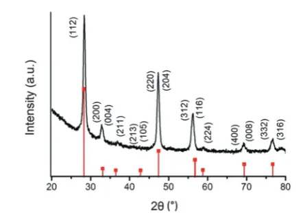
Fig. 1 The p-XRD patterns of CZTS nanoparticles synthesised at 2201C for 1 hour. The reference patterns are of kesterite CZTS (ICDD: 04-015-0223). The TEM images showed hexagonal particles with an average size of 102 nm. The high resolution TEM (HRTEM) images shown in Fig. 2a and b, exhibit clear lattice fringes with measuredd-spacing ofca.0.313(1) nm corresponding to the (112) lattice plane of the kesteritic CZTS structure (Fig. 2c). The elemental composition of the CZTS nanocrystals was determined by energy dispersive X-ray spectroscopy (EDX), which gave a Cu/Zn/Sn/S composition (atomic%) of Cu (28.43%), Zn (11.38%), Sn (12.85%) and S (47.34%).
Open Access Article. Published on 05 May 2016. Downloaded on 13/09/2016 12:28:42.
This article is licensed under a
[image:2.595.313.533.468.623.2]decomposition starting at 2841C (1), 3031C (2) and 3001C (3),
all leading to their corresponding metal sulphides. The mid-point of each decomposition is within 51C of 3301C. These TGA results
for complexes (1), (2) and (3) match well with our previous reports.28 The difference in the decomposition temperatures
between this work and earlier reports may be due to the method of reporting or experimental differences.
The p-XRD pattern (Fig. 1) of the sample prepared at 2201C
for 1 hour shows main peaks atd-spacings of: 3.14, 2.73, 1.92, 1.64, 1.35, 69.34 and 1.24 for the (112), (200), (204), (312), (400) and (316) spacings of kesterite CZTS (ICDD: 04-015-0223).24The p-XRD patterns of samples formed at other temperatures are shown in the ESI†(Fig. S1).
The stoichiometry of the material is Cu2.5Zn1Sn1.1S4, which is
slightly Cu rich (however Cu grids were used for the TEM). Fig. 2d shows the selected area elemental map for the nanoparticles synthesised at 2201C; it shows a uniform distribution of the
elements in the entire area of analysis.
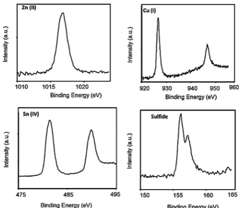
The valence state of the elements in the nanoparticles synthesised at 2201C were determined by XPS (Fig. 3); binding
energies were as follows: Zn 2p3/2, 1017 eV; Cu 2p3/2, 926 eV;
Cu 2p1/2, 947 eV; Sn 3d5/2, 480 eV; Sn 3d3/2, 491 eV; S 2p3/2,
156 eV; S 2p1/2158 eV. The values are commensurate with the
valence states Cu(I), Sn(IV), Zn(I) and S2.25
Organic field-effect transistors
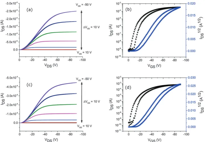
The details of OFET fabrication using both 5T-TTF and P3HT organic semiconductors are given in the experimental section. The results for OFETs fabricated using 5T-TTF are summarised below in Table 1. OFETs fabricated using only 5T-TTF show an average hole mobility of 9.5 103 cm2 V1 s1, which is similar to that determined previously.26The output and trans-fer characteristics for the devices tested are shown below in Fig. 4a and b. The current response is increased (Fig. 4c) for the OFET fabricated using 5 wt% CZTS and the hole mobility calculated is 0.016 cm2 V1 s1, a 68% increase with respect to the device fabricated using pristine 5T-TTF. The ION/IOFF
ratio remains the same for both devices. When the nanoparticle concentration is increased, there is no saturation observed in the output graph. In order to investigate the OFET performance further, AFM was used in tapping mode to characterise the surface morphology of the different devices; these images are
Fig. 2 (a) and (b) are the HRTEM images, (c) the diffraction patterns and (d) the elemental map of CZTS nanoparticles synthesised at 2201C. The scale bar shown for the elemental map isca.50 nm.
[image:3.595.309.546.47.252.2]Fig. 3 High resolution XPS spectra of CZTS nanoparticles synthesised at 2201C.
Table 1 Data for OFETs fabricated from 5T-TTF with various concentra-tions of CZTS nanoparticles
Compound VTh(V)
ON/OFF ratio
Averagemhole (cm2V1s1) sm
hole
5T-TTF 13 103 9.5103 5.8103
5T-TTF + 1% CZTS 17 103 8.5103 3.8103
5T-TTF + 2.5% CZTS 17 103 8.3103 4.6103
5T-TTF + 5% CZTS 15 103 0.016 4.6103
5T-TTF + 10% CZTS — — —
Open Access Article. Published on 05 May 2016. Downloaded on 13/09/2016 12:28:42.
This article is licensed under a
[image:3.595.49.285.283.681.2] [image:3.595.302.554.644.717.2]shown in Fig. 5. The surface of the OFET fabricated using 5T-TTF is comparable to the image of the surface from the previously fabricated device.26Surprisingly, despite the increased roughness of the surface of the device fabricated with 5 wt% CZTS, compared to the pristine organic film, the hole mobility is higher. As the concentration of CZTS is increased to 10%, there is a significant change in morphology with the 5T-TTF domains being broken up. The emergence of a number of gaps in the film explains the poor performance for this device.
The behaviour of the OFETs fabricated using P3HT and CZTS is slightly different to those from 5T-TTF and the device data for each OFET are summarised in Table 2. The output and transfer characteristics for the OFET fabricated using P3HT without any additives are shown in Fig. 6a and b. The average hole mobility calculated for P3HT is 0.041 cm2V1s1and in a similar trend to the 5T-TTF OFET, when 5 wt% CZTS is added to the solution used for OFET fabrication there is an increase in
the mobility. The output and transfer graphs for this device are shown in Fig. 6c and d. The calculated hole mobility (0.053 cm2 V1 s1) is 29% higher than the OFET fabricated without any nanoparticles. However, unlike the oligomer based OFETs where 10% CZTS led to a deterioration in performance, OFETs fabricated with P3HT and 10% CZTS (Fig. 6e and f) showed a further increase in charge carrier mobility, with the
Fig. 4 (a) and (b) show the output and transfer characteristics for an OFET fabricated using 5T-TTF; (c) and (d) are the output and transfer characteristics for an OFET fabricated with 5T-TTF + 5% CZTS.
[image:4.595.118.479.48.297.2]Fig. 5 AFM images of OFETs fabricated from 5T-TTF (left), 5T-TTF + 5% CZTS (centre) and 5T-TTF + 10% CZTS (right)
Table 2 Results for fabricated OFETs from P3HT with various concentra-tions of CZTS
Compound VTh(V)
ON/OFF ratio
Averagemhole
(cm2V1s1) smhole
P3HT 8 102 0.041 0.015
P3HT + 5% CZTS 9 102 0.053 0.012
P3HT + 10% CZTS 10 102 0.088 0.013
P3HT + 15% CZTS 10 102 0.037 9.6103
P3HT + 20% CZTS 10 102 0.033 0.016
Open Access Article. Published on 05 May 2016. Downloaded on 13/09/2016 12:28:42.
This article is licensed under a
[image:4.595.60.552.330.480.2] [image:4.595.303.553.539.618.2]average mobility calculated as 0.088 cm2 V1 s1, a 115% increase compared to the value for the device fabricated using only the polymer. In contrast, a further increase in nanoparticle concentration to 15% or 20% shows charge carrier mobilities only slightly lower than the OFET fabricated with a neat P3HT film, showing that performance is not enhanced by the addition of higher concentrations of nanoparticles.
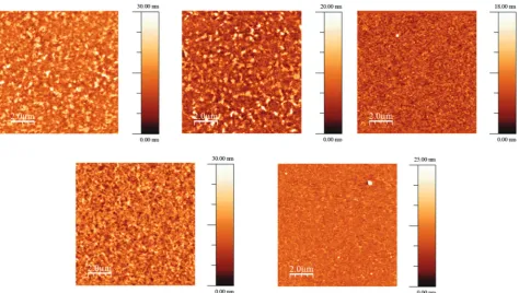
The AFM images for P3HT devices are shown in Fig. 7 and give a clear trend. The device fabricated using neat P3HT shows a number of polymer aggregates on the surface. As 5 wt% CZTS is added to the solution, the resulting device still shows P3HT aggregates, but overall there are fewer of these domains. There is a further reduction in the surface roughness as the CZTS concentration is increased to 10% and there appears to be a significant decrease in the size of the P3HT aggregates. The domain sizes are slightly larger when the concentration is
increased to 15% CZTS and the surface roughness also increases, but the aggregates are smaller than those present in the neat polymer film. This suggests that, although the P3HT aggregates are being broken up in films formed from 15% and 20% CZTS solutions, charge transport is inhibited by the increased nano-particle concentration and therefore leads to a charge carrier mobility that is slightly reduced with respect to OFETs fabricated using P3HT. It is worth noting that the OFET performance does not tail off as significantly as when the CZTS concentration is increased for 5T-TTF containing OFETs.
Finally, in an attempt to determine if the nanoparticles or the oleylamine ligands are responsible for the improved performance, P3HT OFETs were fabricated using 5% v/v and 10% v/v oleylamine. The output and transfer characteristics for each of these OFETs are shown in the ESI†(Fig. S2). The addition of 5% oleylamine leads to a severely reduced mobility (mh= 2.83 103cm2V1s1) and
Fig. 6 Output and transfer characteristics (left and right columns, respectively), for OFETs fabricated using neat P3HT [(a) and (b)], P3HT + 5% CZTS [(c) and (d)], and P3HT + 10% CZTS [(e) and (f)].
Open Access Article. Published on 05 May 2016. Downloaded on 13/09/2016 12:28:42.
This article is licensed under a
[image:5.595.72.534.256.693.2]although this is improved with 10% oleylamine (mh = 6.07
103cm2V1s1), the performance of both devices is considerably poorer than any of the devices fabricated using P3HT and CZTS. This would suggest that the nanoparticles are responsible for improving the OFET performance rather than the long oleylamine ligands.
Conclusion
CZTS nanoparticles have been used as additives for the fabrication of solution-processed OFETs. The nanoparticle composites (5% CZTS) with 5T-TTF had a hole mobility 68% higher than devices using only the oligomer, whilst 10% addition to P3HT devices led to a hole mobility more than double (115% increase) that of the OFET with neat P3HT. The additives are inexpensive and environmentally benign, which suggests that they have potential for the improvement of OFETs. Reports on applications of inorganic nanoparticles in OFETs are sparse in the literature and have been limited mainly to their use as nanocomposites in gate dielectric layers.29–31Zinc oxide nanoparticles have been used in polyfluorene composites for light-emitting field effect transistors,32whilst Q-ZnO has been applied as a component in a hybrid OFET bilayer device fabricated with P3HT as the organic film.33Blends of P3HT and CdSe have been studied in
OFETs34and also in organic photovoltaics devices.35However, the mechanism of charge transport in these composites is not well understood. It has been shown by low temperature light-induced electron spin resonance studies that the morphology of P3HT changes in the presence of CdSe nanoparticles34and that charge transfer between the two components only takes place efficiently if
the CdSe capping ligand is removed. In OFETs, however, the structure of the capping ligand in P3HT/CdSe composites influences the value of the mobility.35This begs the question whether or not the inorganic nanoparticles in hybrid OFETs change the characteristics of the device as a function of morphology or if the role of the inorganic material is more complex. It is perhaps more intuitive to assume the former and our work clearly shows that morphology changes with different loadings of CZTS nanoparticles. However, an in-depth study needs to be conducted to elucidate the full role of CZTS in composites. One would expect that the inclusion of nanoparticles into pristine molecular (5T-TTF) and polymeric (P3HT) materials would disrupt long-range order and affect charge transport detrimentally, and remarkably we see an enhancement of hole mobility upon the application of CZTS nanoparticles. One possible explanation is that the inorganic material reduces the density of traps in the organic layer and this has been seen in the case of MEH-PPV/ZnO blends.36
Acknowledgements
P. K. thanks the School of Chemistry, The University of Manchester for funding. We thank EPSRC for funding the instruments under grant number (EP/K039547/1) for characterisation of the CZTS compounds. P. J. S. thanks the Royal Society for a Wolfson Research Merit Award. R. G. D. T. thanks the EPSRC for funding (EP/L012200/1). All data supporting this research are openly available from http://dx.doi.org/10.15129/2527c5db-bde6-48cd-b145-55f15f837fb2.
Fig. 7 AFM images for OFETs fabricated using P3HT (top, left), P3HT + 5% CZTS (top, centre), P3HT + 10% CZTS (top, right), P3HT + 15% CZTS (bottom, left) and P3HT + 20% CZTS (bottom, right).
Open Access Article. Published on 05 May 2016. Downloaded on 13/09/2016 12:28:42.
This article is licensed under a
[image:6.595.62.537.47.315.2]Notes and references
1 Y. Qiao, Y. Guo, C. Yu, F. Zhang, W. Xu, Y. Liu and D. Zhu,
J. Am. Chem. Soc., 2012,134, 4084–4087.
2 R. Pfattner, M. Mas-Torrent, I. Bilotti, A. Brillante, S. Milita, F. Liscio, F. Biscarini, T. Marszalek, J. Ulanski, A. Nosal, M. Gazicki-Lipman, M. Leufgen, G. Schmidt, L. W. Molenkamp, V. Laukhin, J. Veciana and C. Rovira, Adv. Mater., 2010,22, 4198–4203.
3 E. D. Głowacki, M. Irimia-Vladu, M. Kaltenbrunner, J. Gsiorowski, M. S. White, U. Monkowius, G. Romanazzi, G. P. Suranna, P. Mastrorilli, T. Sekitani, S. Bauer, T. Someya, L. Torsi and N. S. Sariciftci,Adv. Mater., 2013,25, 1563–1569.
4 H.-R. Tseng, H. Phan, C. Luo, M. Wang, L. A. Perez, S. N. Patel, L. Ying, E. J. Kramer, T.-Q. Nguyen, G. C. Bazan and A. J. Heeger,
Adv. Mater., 2014,26, 2993–2998.
5 I. Meager, M. Nikolka, B. C. Schroeder, C. B. Nielsen, M. Planells, H. Bronstein, J. W. Rumer, D. I. James, R. S. Ashraf, A. Sadhanala, P. Hayoz, J.-C. Flores, H. Sirringhaus and I. McCulloch,Adv. Funct. Mater., 2014,24, 7109–7115.
6 S. Park, B. T. Lim, B. Kim, H. J. Son and D. S. Chung,
Sci. Rep., 2014,4, 5482.
7 Y. Yuan, G. Giri, A. L. Ayzner, A. P. Zoombelt, S. C. B. Mannsfeld, J. Chen, D. Nordlund, M. F. Toney, J. Huang and Z. Bao,Nat. Commun., 2014,5, 3005.
8 J. Huang, D. R. Hines, B. J. Jung, M. S. Bronsgeest, A. Tunnell, V. Ballarotto, H. E. Katz, M. S. Fuhrer, E. D. Williams and J. Cumings,Org. Electron., 2011,12, 1471–1476.
9 M. El Gemayel, A. Narita, L. F. Dossel, R. S. Sundaram, A. Kiersnowski, W. Pisula, M. R. Hansen, A. C. Ferrari, E. Orgiu, X. Feng, K. Mullen and P. Samori,Nanoscale, 2014,
6, 6301–6314.
10 S. Park, S. Jin, G. Jun, S. Jeon and S. Hong,Nano Res., 2011,
4, 1129–1135.
11 Y. D. Park, J. A. Lim, Y. Jang, M. Hwang, H. S. Lee, D. H. Lee, H.-J. Lee, J.-B. Baek and K. Cho, Org. Electron., 2008, 9, 317–322.
12 X.-Z. Bo, C. Y. Lee, M. S. Strano, M. Goldfinger, C. Nuckolls and G. B. Blanchet,Appl. Phys. Lett., 2005,86, 182102. 13 P. Jackson, D. Hariskos, E. Lotter, S. Paetel, R. Wuerz,
R. Menner, W. Wischmann and M. Powalla, Prog. Photo-voltaics, 2011,19, 894–897.
14 W. Wang, M. T. Winkler, O. Gunawan, T. Gokmen, T. K. Todorov, Y. Zhu and D. B. Mitzi,Adv. Energy Mater., 2014,4, 1301465. 15 W. Yang, H.-S. Duan, K. C. Cha, C.-J. Hsu, W.-C. Hsu,
H. Zhou, B. Bob and Y. Yang,J. Am. Chem. Soc., 2013,135, 6915–6920.
16 B. Shin, O. Gunawan, Y. Zhu, N. A. Bojarczuk, S. J. Chey and S. Guha,Prog. Photovoltaics, 2013,21, 72–76.
17 H. Zhou, H.-S. Duan, W. Yang, Q. Chen, C.-J. Hsu, W.-C. Hsu, C.-C. Chen and Y. Yang, Energy Environ. Sci., 2014,7, 998–1005.
18 L. Arora, V. Singh, G. Partheepan, T. D. Senguttuvan and K. Jain,Appl. Nanosci., 2015, 1–10.
19 G. Konstantatos, I. Howard, A. Fischer, S. Hoogland, J. Clifford, E. Klem, L. Levina and E. H. Sargent, Nature, 2006,442, 180–183.
20 J. M. Luther, M. Law, Q. Song, C. L. Perkins, M. C. Beard and A. J. Nozik,ACS Nano, 2008,2, 271–280.
21 G. I. Koleilat, L. Levina, H. Shukla, S. H. Myrskog, S. Hinds, A. G. Pattantyus-Abraham and E. H. Sargent, ACS Nano, 2008,2, 833–840.
22 N. Revaprasadu, M. A. Malik and P. O’Brien,S. Afr. J. Chem., 2004,57, 40–43.
23 M. B. Hursthouse, M. A. Malik, M. Motevalli and P. O’Brien,
J. Mater. Chem., 1992,2, 949–955.
24 K. Ramasamy, V. L. Kuznetsov, K. Gopal, M. A. Malik, J. Raftery, P. P. Edwards and P. O’Brien, Chem. Mater., 2013,25, 266–276.
25 A. V. Moholkar, S. S. Shinde, G. L. Agawane, S. H. Jo, K. Y. Rajpure, P. S. Patil, C. H. Bhosale and J. H. Kim,
J. Alloys Compd., 2012,544, 145–151.
26 I. A. Wright, N. J. Findlay, S. Arumugam, A. R. Inigo, A. L. Kanibolotsky, P. Zassowski, W. Domagala and P. J. Skabara,
J. Mater. Chem. C, 2014,2, 2674–2683.
27 S. Ji, T. Shi, X. Qiu, J. Zhang, G. Xu, C. Chen, Z. Jiang and C. Ye,Sci. Rep., 2013,3, 2733.
28 K. Ramasamy, M. A. Malik and P. O’Brien,Chem. Sci., 2011,
2, 1170–1172.
29 M. R. Beaulieu, J. K. Baral, N. R. Hendricks, Y. Tang, A. L. Brisen˜o and J. J. Watkins,ACS Appl. Mater. Interfaces, 2013,5, 13096–13103.
30 L. Huang, Z. Jia, I. Kymissis and S. O’Brien, Adv. Funct. Mater., 2010,20, 554–560.
31 R. P. Ortiz, A. Facchetti and T. J. Marks,Chem. Rev., 2010,
110, 205–239.
32 N. A. Andrey and P. S. Igor, J. Phys. D: Appl. Phys., 2010,
43, 315104.
33 R. A. Picca, M. C. Sportelli, D. Ho¨tger, K. Manoli, C. Kranz, B. Mizaikoff, L. Torsi and N. Cioffi,Electrochim. Acta, 2015,
178, 45–54.
34 U. Bielecka, P. Lutsyk, M. Nyk, K. Janus, M. Samoc, W. Bartkowiak and S. Nespurek,Mater. Sci.-Pol., 2013,31, 288–297.
35 M. D. Heinemann, K. von Maydell, F. Zutz, J. Kolny-Olesiak, H. Borchert, I. Riedel and J. Parisi,Adv. Funct. Mater., 2009,
19, 3788–3795.
36 Z.-X. Xu, V. A. L. Roy, P. Stallinga, M. Muccini, S. Toffanin, H.-F. Xiang and C.-M. Che,Appl. Phys. Lett., 2007,90, 223509.
Open Access Article. Published on 05 May 2016. Downloaded on 13/09/2016 12:28:42.
This article is licensed under a
![Fig. 6Output and transfer characteristics (left and right columns, respectively), for OFETs fabricated using neat P3HT [(a) and (b)], P3HT + 5% CZTS[(c) and (d)], and P3HT + 10% CZTS [(e) and (f)].](https://thumb-us.123doks.com/thumbv2/123dok_us/1533474.105948/5.595.72.534.256.693/output-transfer-characteristics-columns-respectively-ofets-fabricated-czts.webp)