Carrier Localization in the Vicinity of Dislocations in InGaN
F.C-P. Massabuau,1,a) P. Chen,1 M.K. Horton,2, 3 S.L. Rhode,3 C.X. Ren,1 T.J. O’Hanlon,1 A. Kov´acs,4 M.J. Kappers,1 C.J. Humphreys,1 R.E. Dunin-Borkowski,4 and R.A. Oliver1
1)Department of Materials Science and Metallurgy, University of Cambridge,
Cambridge, UK
2)Materials Science Division, Lawrence Berkeley National Laboratory, Berkeley,
US
3)Department of Materials, Imperial College London, London,
UK
4)Ernst Ruska-Centre for Microscopy and Spectroscopy with Electrons
and Peter Gr¨unberg Institute, Forschungszentrum J¨ulich GmbH, J¨ulich,
Germany
We present a multi-microscopy study of dislocations in InGaN, whereby the same
threading dislocation was observed under several microscopes (atomic force
mi-croscopy, scanning electron mimi-croscopy, cathodoluminescence imaging and
spec-troscopy, transmission electron microscopy), and its morphological optical and
struc-tural properties directly correlated. We achieved this across an ensemble of defects
large enough to be statistically significant. Our results provide evidence that carrier
localization occurs in the direct vicinity of the dislocation through the enhanced
for-mation of In-N chains and atomic condensates, thus limiting non-radiative
recombi-nation of carriers at the dislocation core. We highlight that the localization properties
in the vicinity of threading dislocations arise as a consequence of the strain field of
the individual dislocation and the additional strain field building between interacting
neighboring dislocations. Our study therefore suggests that careful strain and
dis-location distribution engineering may further improve the resilience of InGaN-based
devices to threading dislocations. Besides providing a new understanding of
disloca-tions in InGaN, this paper presents a proof-of-concept for a methodology which is
relevant to many problems in materials science.
PACS numbers: 68.37.Hk, 68.37.Lp, 68.37.Ma, 68.37.Og, 68.37.Ps, 78.60.Hk, 78.66.Fd
I. INTRODUCTION
Owing to a direct band gap ranging from the ultraviolet (Eg GaN = 3.51 eV) to the infrared
(Eg InN = 0.7 eV)1, InxGa1−xN (which for convenience we abbreviate to InGaN) has become
the leading semiconductor for numerous optoelectronic applications. Whilst thin layers of
InGaN (thickness below ∼5 nm) are employed in the active region of light emitting diodes
(LEDs), as quantum wells (QWs)2,3, thick layers of InGaN (thickness above 20 nm) find application as the active region in solar cells4–7, as prelayers located under the InGaN/GaN QW stack in LEDs8–10 or as sacrificial layers for example in the fabrication of microdisk11 or nanobeam12 lasers.
However this material is characterized by a high density of threading dislocations, which
are commonly associated with non-radiative recombination centers13–17. Threading dislo-cations in InGaN fall into three categories depending on their Burgers vector, b, namely
edge-type (b =a), mixed-type (b = a +c) and screw-type (b =c) dislocations, and have
been reported to be terminated by V-shaped pits18. However InGaN-based devices are sur-prisingly resilient to the presence of such high densities of threading dislocations. Several
mechanisms have been suggested to explain this resilience19 but the role of dislocations in InGaN is still ambiguous and poorly understood.
In this study we observed the same threading dislocation in a thick layer of InGaN
under different microscopes, namely atomic force microscopy (AFM), scanning electron
mi-croscopy (SEM), cathodoluminescence (CL) and transmission electron mimi-croscopy (TEM).
This approach, referred to as “multi-microscopy”20, allowed us to directly correlate the mor-phological, optical and structural properties of that specific dislocation. We observed an
enhancement of the CL emission at the center of the V-pits, which could be ascribed to
an enhanced formation of In-N chains and atomic condensates and localize carriers in the
vicinity of the dislocation core. The correlation of these multiple microscopy techniques
al-lowed us to link the carrier localization properties to the strain of the individual dislocation
as well as to that arising from the interaction of neighboring dislocations, while showing no
II. EXPERIMENTAL METHODS
A. Sample Growth and Characterization
A Si-doped InGaN epilayer was grown by metal-organic vapor phase epitaxy (MOVPE)
in a Thomas Swan 6 ×2 inch close-coupled showerhead reactor. Trimethylgallium (TMG),
trimethylindium (TMI), diluted silane in hydrogen (SiH4) and ammonia (NH3) were used
as precursors for the Ga, In, Si and N elements, respectively. Hydrogen (H2) was used as the carrier gas for the growth of GaN, while a mixture of hydrogen and nitrogen (N2) was employed for InGaN growth. Pseudo-substrates consisting of ca. 5 µm of GaN (of which 2
µm undoped and 3µm Si-doped to 5×1018 cm−3) grown on c-plane sapphire with a miscut of 0.25±0.10◦ towards (11¯20) were employed, yielding a threading dislocation density of
4×108 cm−2 approximately. After the growth of a 500 nm thick GaN connecting layer, the InGaN layer was grown at 749◦C using a TMI flow of 8.1 µmol.min−1, a TMG flow of 5.9 µmol.min−1, a SiH4 flow of 0.6 nmol.min−1 resulting in a Si-doping of approximately 5×1018cm−3, a NH
3 flow of 446 mmol.min−1, and a H2 flow rate of 200 sccm (standard cubic centimetre per minute) to improve the surface quality21. The thickness and composition of the InGaN layer were obtained by X-ray diffraction (XRD) on a Philips X-pert MRD
diffractometer, using a four-bounce Ge(220) monochromator and a three-bounce Ge(220)
analyzer crystal. Analysis of the symmetric 002 reflection yields a thickness of the InGaN
layer of 136±2 nm and an indium composition of x = 8.6±0.5%. Reciprocal space maps
taken around the symmetric 006 and asymmetric 204 reflections revealed that the InGaN
layer is fully strained on the GaN pseudo-substrate. The sample was prepared for
multi-microscopy analysis using the set-up described in earlier work20, consisting of a copper grid, as is used in TEM sample preparation, positioned at the surface of the sample. Using the
50 µm size square mesh as well as the trench defects at the surface of the sample (basal
plane stacking fault bounded by a vertical stacking mismatch boundary which opens up at
the sample surface as a trench enclosing a region of material)22–24, the same V-defects could be easily identified in the different microscopes: AFM, SEM, CL and high angle annular
dark-field scanning TEM (HAADF-STEM). About 600 dislocations have been analyzed by
AFM and SEM-CL, and about 30 of them have been observed at the atomic scale by TEM.
SEM-CL, TEM sample preparation, TEM.
B. Analysis of AFM data
AFM, performed on a Veeco Dimension 3100 operating in tapping mode, was used to
determine the dislocation type and the distance to nearest neighbor of each of the 600
dislocations. In III-Nitrides, threading dislocations have their line direction parallel to [0001]
and fall into in three categories depending on their Burgers vector. Therefore a-type,
ctype and a+cctype dislocations respectively edge, screw and mixedctype dislocations
-have a Burgers vector b = 1/3 h11¯20i, b = [0001] and b = 1/3 h11¯23i, respectively25. The dislocation type can be determined by AFM using the diameter of the V-pit which
terminates the dislocation26. The diameter of the V-defects was measured as the distance between the two sides of the pit taken 4 nm below the average level of the surrounding
material. It is worth noting that in order to reduce the impact of the tip status on our
measurements, all the AFM images were taken using the same fresh tip. Using this method,
two distinct populations of V-defects can be directly identified, one type of pits of smaller
diameter identified as V-pits originating from edge-type dislocations and the other type of
larger diameter corresponding to mixed-type dislocations. Finally a third group can be
observed, with a diameter greater than that of the other two populations, and relates to
V-pits originating from screw-type dislocations. The ratio of edge, mixed and screw-type
dislocations is 55%, 45% and <1%, respectively, in agreement with results from studies
carried out on similar pseudo-substrates26,27. It should be noted that only 2 out of the 600 dislocations are of pure screw character, and therefore are not discussed here due to their
poor statistical relevance.
C. Analysis of SEM-CL data
SEM-CL was conducted at room temperature using an FEI field emission gun XL30 SEM,
and coupled with a Gatan MonoCL4 CL system. The spatial resolution of CL measurements
is a function of several factors (including probe size, interaction volume size, and carrier
This results in the CL signal to originate from 0.3 RKO∼30-40 nm below the surface30(which
corresponds to the depth at which the electron energy-loss profile reaches a maximum).
Taking into account the absorption of an emitted photon by the material (which is generally
quite high for III-Nitrides, with a typical absorption coefficient of∼105cm−1)31, the majority of the CL signal collected must arise from the first 25-30 nm of material below the surface.
This value was confirmed using a Monte Carlo simulation32. The slits and diffraction grating of the CL system were set at 0.2 mm and 1200 lines/mm, respectively, thus allowing a
0.5 nm spectral resolution. The light emission was recorded between 370 nm to 430 nm
approximately, with the peak emission of the sample being at 406 nm. For each of the
V-pits previously observed by AFM, a series of CL emission spectra were recorded along a
line scan crossing the V-pit, about 500 nm long and with a pitch of 25 nm approximately
(i.e. comparable to the lateral size of the interaction volume). For each line spectra across
a V-pit, the data analysis was performed as follows. Each spectrum was first fitted using
a single Gaussian function. The central wavelength and intensity of the Gaussian fits were
then recorded and plotted as a function of the probe position. The pixels allocated to the
V-pit were firstly identified and then the remaining pixels - allocated to the surrounding
material only - were fitted by a third order polynomial function. This allowed us to fit the
variations in intensity and peak emission wavelength of the material surrounding the V-pit.
(Given that the intensity and peak emission of the surrounding material, non-affected by
the presence of V-pits, is not uniform across the sample, for example because of the presence
of compositional or strain fluctuations, additional line spectra similar in length and pixel
size were recorded on regions unaffected by the V-pits. This allowed the determination of
the best fit for the fluctuations in wavelength and intensity of the material surrounding the
V-pits, showing the third-order polynomial to be the most suitable approach.) The data
thus recorded to characterize each V-pit are the “energy shift”, measured as the difference in
emission energy between the experimental data and the “surrounding” polynomial fit taken
at the position of the center of the pit, and on the facets of the pit, and the “intensity ratio”,
measured as the ratio between the intensity of the experimental data and the “surrounding”
D. Analysis of TEM data
The sample was prepared for plan-view imaging in the TEM using standard mechanical
polishing method followed by Ar+ion milling at 5 kV and cleaning at 1 kV. Finally, acetone and a dilute solution of nitric acid were used to clean the sample from thermal wax and from
sputtering of material back to the TEM foil during the ion milling process. HAADF-STEM
was performed on an FEI Titan G2 80-200 with a detector collection semi-angle of 69 mrad.
In order to prevent electron beam damage in the TEM33,34, the microscope was operated at 80 kV, which is below the knock-on threshold for InGaN34. The threading dislocations could be easily identified in ADF-STEM contrast due to the foil thickness reduction induced
by the presence of a V-pit at their termination, resulting in a sudden change in contrast.
The dislocations were observed along the [0001] zone-axis (i.e. parallel to the dislocations
line direction), thus allowing identification of the core structure27,35.
III. RESULTS AND DISCUSSION
A. Multi-microscopy proof-of-concept
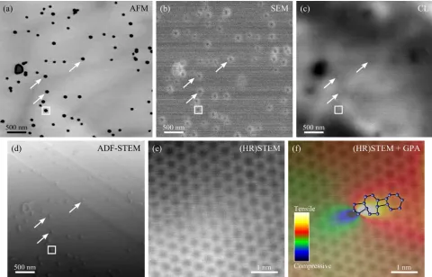
Figure 1 gives an example of multi-microscopy observation of dislocations in InGaN which
demonstrates the ability to perform a one-to-one analysis of the same threading dislocations
by AFM, SEM, CL and TEM. In several cases the dislocations have been observed at the
atomic scale, where the core structure as well as the strain domains around the dislocation
could be identified (Figure 1(e)-(f)). It should be noted that the GPA is used here only
qualitavely, as an illustration of the regions of tensile and compressive strain around the
dislocation core. One can see that the V-pits, directly observable on the AFM and SEM
pictures (Figure 1(a)-(b)), coincide with bright spots surrounded by a darker halo in the CL
image (Figure 1(c)). This observation indicates enhanced light emission properties from the
central part of the V-pit, where the dislocation is located, in contrast to previous reports
which only observed dark spots by CL and therefore concluded that dislocations are
non-radiative recombination centers13–15.
The correlation between the AFM measurements (which give “dislocation type”, i.e.
edge-, mixed- or screw-type, and “distance to nearest neighbor”, i.e. smallest distance
FIG. 1. AFM (a), SEM (b), panchromatic CL (c), and ADF-STEM (d) performed on the same
micrometre-scale area. To guide the eye, a few dislocations are indicated by arrows in each picture. (e) High-resolution (HR) STEM image of the dislocation indicated by a square in (a)-(d), enabling
the identification of the core structure (here dissociated 7/4/8/5-atom ring), and (f) geometric phase analysis (GPA) showing the xx strain component of the dislocation core region.
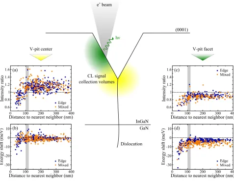
SEM-CL measurements (“intensity ratio” and “energy shift” from different parts of the
V-pit, i.e. emission intensity and energy relative to the surrounding material) is illustrated in
Figure 2. (It should be noted that no correlation was found between the diameter of the
V-pit and the emission properties recorded at the center of the V-V-pit (yellow region in Figure 2)
or from its facet (green region in Figure 2), hence we believe that the results we present here
are not an artefact due to a difference in light extraction efficiency between the V-pit and
its surroundings. Additionally, the fact that both energy shift and intensity ratio depend
on nearest neighbor distance also indicates that this is not an extraction efficiency effect,
since roughening induced increases in extraction efficiency do not lead to energy shifts.)
FIG. 2. Schematic showing the electron probe in the SEM-CL scanning across a V-pit. The scale of the schematic, although indicative, is representative of the experimental conditions in which the
experiment was conducted. Distance to nearest neighbor dependence of the intensity ratio (a)(c) and energy shift (b)(d) measured at the center (a)(b) and facet (c)(d) of the V-pits.
ratio and energy shift can be observed to increase as the distance to nearest neighboring
dislocation increases before reaching a plateau. In all the graphs the transition between the
two regimes occurs for dislocation separations of 100-120 nm, as indicated by the grey bars
in Figure 2. For convenience we will refer to the threading dislocations with spacing below
100 nm as “clustered dislocations”, and to those with spacing above 120 nm as “isolated
B. Investigation of isolated dislocations
Looking in more detail at the properties of isolated dislocations, it can be seen that the
intensity ratio measured in the center of the V-pit (i.e. in the close vicinity of the dislocation
core) is above unity (Figure 2(a)), which is in line with the enhanced luminescence shown in
Figure 1(c). On average, the emission intensity is increased by 15% with a standard deviation
σ = 10% for isolated edge-type dislocations, and by 17% (σ = 13%) for isolated mixed-type
dislocations. (Note that the standard error here is under 1%, but standard deviations are
quoted to indicate the width of the distribution). This result suggests an increase in the
radiative recombination rate occurring in the vicinity of the dislocation core. It can also be
noted that the energy shift remains close to zero (Figure 2(b)). The shift from the center
of the V-pit is -1 meV (σ = 2 meV) for isolated edge-type dislocations, with minimum and
maximum values of -5 meV and +9 meV, respectively. For isolated mixed-type dislocations
this shift is -1 meV (σ = 2 meV) with minimum and maximum values of -7 meV and +7
meV, respectively. On the other hand, on the facets of the V-pit the intensity ratio remains
below unity (Figure 2(c)) whereby we note a reduction of the CL emission by 9% (σ = 4%)
for isolated edge-type dislocations and 11% (σ = 6%) for isolated mixed-type dislocations.
The energy shift is almost always observed to be negative (i.e. emission redshifted compared
to the surrounding material), -3 meV (σ= 1 meV) for edge-type dislocations with minimum
and maximum values of -9 meV and +1 meV, respectively. For mixed-type dislocations the
shift is -6 meV (σ = 2 meV) with minimum and maximum values -12 meV and -1 meV,
respectively (Figure 2(d)). It is worth pointing out that except in the case of the energy
shift measured on the facets, the optical properties have no measureable dependence on
the dislocation type. It can then be inferred that the mechanism explaining the emission
properties of the dislocation itself is distinct from that determining the properties of the
facets of the V-pit which forms at its apex. Given the local character of the properties we
report (i.e. variations on a lateral scale of a few nms), as well as the energy shifts involved
in this experiment (i.e. a few meVs), two main mechanisms can be considered: strain
relaxation36,37 and formation of In-N chains and atomic condensates38–40 (in short “In-N chains”).
Using XRD the InGaN layer was found to be, on average, fully strained on the GaN
dislocation disturbs the strain state locally. Indeed the dislocation is bordered by a region
of higher strain - i.e. compressive region - and a region of lower strain - i.e. tensile region
- as illustrated in Figure 1(f). Additionally, dislocations in InGaN form V-pits as a means
to reduce the strain in the material36, thus leading to a local strain relaxation around the facets of the V-pit. A variation in strain commonly induces a variation in the transition
energy in the material. Indeed a recent study performed on a number of thick InGaN
films reported that the band gap bowing parameter varied as a function of the relaxation37. Based on the values of bowing reported in this study, a full relaxation of the InGaN would
induce a decrease in the emission energy of 129 meV in our sample. Hence a (local) partial
relaxation of the material could lead to a redshift of the CL emission similar to what we
report. It is worth noting that we do not ascribe the CL emission properties to a different
indium incorporation on the facets of the V-pit as compared to the surrounding material
because the energy shift is observed to vary with dislocation type, which cannot be easily
explained by mechanisms other than strain relaxation. Besides, the compositional variations
required to cause such low energy shifts must be<<1%. Therefore, we attribute the emission
properties of the facet of the V-pit, whereby the emission intensity is poorer than that of the
surrounding material, and the energy shift is almost systematically negative and dependent
on the dislocation type, to strain relaxation occurring on the facets of the V-pit. The
intensity ratio below unity could be explained by a lesser amount of localization centers in
this region, thus leading to a fraction of the carriers to recombine non-radiatively at the
dislocations core.
The presence of In-N chains in the material has been found, theoretically38,39 and experimentally40, to strongly localize holes in InGaN. Using a first-principle density func-tional theory approach on In0.14Ga0.86N alloy, Liuet al. predicted that the formation of In-N zigzag chains and In-N atomic condensates localized the valence band states and reduced
the energy band gap by 20 meV and 100 meV, respectively38. Similarly, Schulz et al. used density functional theory calculations on dilute InGaN alloys to determine the effect of
having one to four indium atoms sharing a same nitrogen atom on carrier localization39. Their results revealed a strong hole wavefunction localization associated by a decrease of the
band gap energy. Compared to a single In-N bond, an In-N chain (i.e. two or more indium
atoms sharing a same nitrogen atom) were found to decrease the band gap energy by 8
Moreover, the excited hole states were localized up to 50 meV from the valence band edge.
Thus an In-N chain or atomic condensate would localize the holes while inducing an energy
shift between approximately +42 meV and -8 meV (two indium atoms), +32 meV and -18
meV (three indium atoms), and +21 meV and -29 meV (four indium atoms). Moreover,
recent studies reported that indium tends to segregate in the tensile part of the core of
threading dislocations in thick InGaN layers35,41. Our data then suggest that the enhanced emission recorded in the center of the V-pit, and the low energy shift independent of the
dislocation type are ascribed to an increase in the number of In-N chains forming in the
vicinity of the dislocation core as a result of the indium segregation reported by Horton et
al. and Rhode et al.35,41. It should be noted that the segregation of indium atoms at the vicinity of the dislocation core was reported to occur within a few nanometers from the core
of the dislocation, and hence does not alter our measurements and conclusions reported on
the V-pit facets.
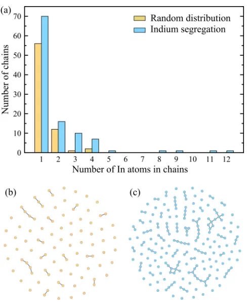
To investigate this hypothesis further, Metropolis Monte Carlo simulations of indium
segregation to a dislocation core were performed to obtain statistical information on the
expected length and distribution of In-N chains if indium segregation occurs relative to
that of a random alloy. To match our sample, the calculation considered a volume of
InGaN of composition 8.6% strained to match a GaN template and containing an edge-type
dislocation. The 5/7-atom ring edge-type core was selected as a representative example,
since there are too many unique core structures in the wurtzite crystal system to do a
systematic analysis of all core types. However, since segregation of comparable magnitudes
is expected for all core types41, this example should prove sufficient. The dimensions of the supercell are 64a × 64a × 16c, with Monte Carlo swaps performed in the vicinity of
a single dislocation core. Equilibrium was said to be obtained after approximately 6×10⁴ trial swaps when the trend in total potential energy stops decreasing and instead fluctuates
around a constant level and the local concentration around the dislocation core stabilized,
although a total of 1.8×10⁵ trial swaps were ultimately performed. Further details on this computational methodology can be found detailed elsewhere41. Graph-tool42 was used to extract additional information from the resulting microstructure. Histograms of the results
are shown in Figure 3, obtained by counting the number and length of In-N chains within
a cylinder of radius 10 ˚A centered on the dislocation core. Alongside the histogram are 2D
FIG. 3. (a) Histogram of the number of In-N chains as a function of the number of indium atoms
in the chains, located within a 10 ˚A radius centered on the dislocation, in the case of a random distribution of indium (i.e. initial configuration of the simulation) or segregation of indium (i.e.
equilibrium configuration of the simulation). Abstract representation of the data in (a), in the case of a random distribution (b) or segregation (c) of indium atoms.
point joined to another point represents an InNIn chain (Figure 3(b) random alloy,(c)
-indium segregation to dislocation core). At equilibrium, a significantly higher proportion of
longer chains can be clearly seen, and in particular a significant proportion of 3-In-containing
and 4-In-containing chains, which would be comparatively rare in a random alloy at this
composition. These results support the proposition that the enhanced emission properties
measured in the center of the V-pit arise from the formation of In-N chains in the vicinity
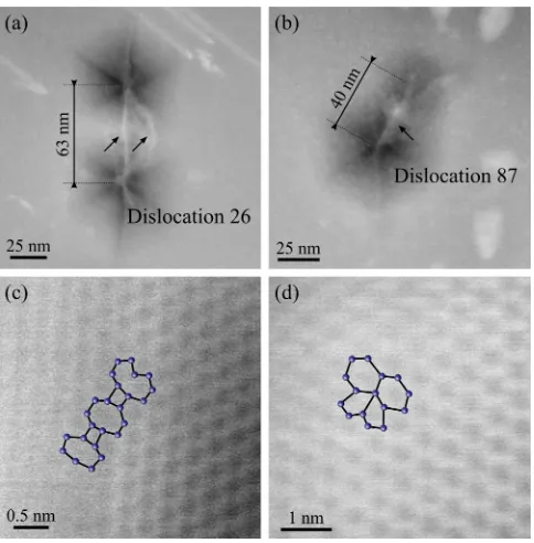
[image:13.612.184.428.66.370.2]FIG. 4. ADF-STEM image of the clustered dislocations 26 (a) and 87 (b). The white strain-related
contrast between the neighboring dislocations is indicated by an arrow. Aberration-corrected HAADF-STEM image of the core of dislocation 26 (dissociated 7/4/8/4/9-atom ring)(c) and 87
(undissociated double 5/6-atom ring)(d). An ABSF-filter (Average Background Subtraction Filter) has been applied to (c) and (d) in order to remove noise from the images.
C. Investigation of clustered dislocations
Figure 2 highlighted different emission properties for those threading dislocations which
have a distance to their nearest neighbor below 100-120 nm - i.e. clustered dislocations. In
this configuration, both the intensity ratio and energy shift were observed to decrease when
the dislocation is closer to its neighbor. For the dataset recorded on the center of the V-pit,
we note a sharp decrease in the intensity ratio down to below unity. Similarly, we record
increasing negative energy shifts, down to -18 meV. For the data taken on the facet of the
V-pit, this phenomenon is even more pronounced with lower intensity ratios and energy shifts
down to -33 meV. Based on our earlier arguments, these observations can be attributed to
a decrease in strain affecting the V-pit globally (facet and center). We tentatively attribute
that decrease in strain to the additional strain field that is generated when two neighboring
dislocations are close enough to interact with each other. The intensity ratio is reduced in
- i.e. the neighboring dislocation - within the CL generation volume. Figure 4 shows
ADF-STEM images of two clustered mixed-type dislocations (referred to as “Dislocation 26” and
“Dislocation 87”). Dislocations 26 and 87 are representative of typical clustered dislocations
having distances to nearest neighbors of 63 nm and 40 nm respectively, intensity ratios in
the center of the V-pit of 0.66 and 0.81 respectively, and energy shifts in the center of the
V-pit of -4 meV and -6 meV respectively. Figure 4(a),(b) highlights the interaction of these
two dislocations with their neighbor. ADF-STEM is an imaging technique which is generally
used for Z-contrast imaging, although the contrast is also sensitive to the strain and to the
foil thickness. A bright contrast (indicated by arrows in Figure 4(a),(b)) can be clearly
observed linking the apices of the two neighboring dislocations, which indicates a change
in strain in the region between the two dislocations compared to the surrounding material.
The geometry of this contrast makes it very unlikely to be Z-related (i.e. indicating an
increase in indium composition), and furthermore the required compositional variation to
achieve such a contrast change would incur a much larger energy shift than that which is
observed. Therefore Figure 4 further confirms that the CL emission properties of clustered
dislocations arise from the additional strain relaxation mechanism due to the proximity of
two (or more) dislocations.
Figure 4 also shows the dislocation core structures of Dislocations 26 (Figure 4(c)) and 87
(Figure 4(d)). It reveals that whilst Dislocation 26 has a dissociated core, with formation of
a 7/4/8/4/9-atom ring, the core of Dislocation 87 is undissociated, with a double 5/6-atom
ring27,35. Despite being both mixed-type, these two dislocations exhibit a fundamentally different core property in which the core of Dislocation 26 dissociated in order to reduce
its energy (through formation of two partial dislocations and a stacking fault)43 while Dis-location 87 did not. One might have suggested that the disDis-location’s core structure may
influence the emission properties of the material in its vicinity. However we saw that the
CL emission properties are quite similar between these two dislocations, therefore indicating
that the impact of the core structure on the optical properties of a dislocation is negligible.
The fact that edge-type dislocations only take one specific core configuration in our sample
(we only observed 5/7-atom ring cores, in agreement with Rhode et al.)27,35, irrespective of the isolated or clustered configuration, but exhibit the same variations in emission properties
FIG. 5. 16K CL integrated intensity (a)(c) and peak emission energy (b)(d) maps of isolated
(a)(b) and clustered (c)(d) dislocations. To guide the eye, the position of the bright spots, directly observable in (a) and (c), is indicated by circles in all the maps. To emphasize the relative variations
in intensity and energy between isolated and clustered configurations, a common color scale is used in (a) and (c) and in (b) and (d).
D. Comparison with liquid He SEM-CL
In order to consolidate our analysis, the sample has been observed by CL in the SEM at a
temperature of 16K. Decreasing the temperature has many advantages; in particular it leads
to a decrease of the non-radiative recombination rate in the material resulting in a dramatic
increase of the CL signal. This consequently enables us to record spectral maps (instead
of spectral lines) with improved spectral resolution (herein 0.2 nm approximately). Figure
5 shows an example of such maps taken around isolated (Figure 5(a)-(b)) and clustered
(Figure 5(c)-(d)) dislocations, and which qualitatively summarizes and corroborates the
measurements reported in Figure 2.
The intensity maps in Figure 5(a),(c) clearly show the presence of a bright spot
sur-rounded by a darker halo at the position of a dislocation, which supports our observations
made by room temperature CL as well as the measurements of intensity ratio reported
ear-lier. The bright spot and the dark halo can be also easily distinguished in the energy map
as their energy domains are distinct. The bright spot - corresponding to the emission from
[image:16.612.184.427.68.265.2]sur-rounding material, as was shown quantitatively in Figure 2(b). In comparison the shift in
energy measured on the facets of the V-pits - the dark halo - is much greater, in line with the
results reported in Figure 2(d). While the emission properties from the center of the V-pit
have been ascribed to the enhanced formation of In-N chains in the tensile region of the
dislocation core, those from the facet of the V-pit have been attributed to strain relaxation.
The possibility of recording CL maps highlights a very interesting feature which supports
this analysis. In Figure 5(b) it can be seen that although a low energy ring surrounds the
position of the dislocations (indicated by a circle), one side of the ring has a significantly
more pronounced energy shift, making the ring appear like a bean partially encircling the
dislocation. This asymmetry is the emission energy signature of the tensile (low energy
side of the ring) and compressive (high energy side of the ring) regions of the dislocation
superimposed on the strain relaxation from the V-pit facets. Finally Figure 5(c)-(d) show
the intensity and emission energy maps recorded around clustered dislocations. Facilitated
by the use of a common color scale with Figure 5(a)-(b), it can be seen that, similar to what
was reported in Figure 2, the intensity ratio is decreased and the energy shift is more
pro-nounced compared to the configuration where the dislocations are isolated. It can be noted
that the low energy domain that in the isolated dislocation case we noted was asymmetric
and bean-shaped, is now much larger and links all the dislocations in the cluster. This
corroborates our earlier observations that the stronger energy shift in clustered dislocations
relates to additional strain relaxation arising from the proximity of the dislocations.
This experiment corroborates our quantitative analysis described in sections A-C. It also
further supports that the phenomena we observed are not due to a light extraction effect
because the relative position of the bright spot to the dark halo - as well as their energy
counterparts - varies between dislocations; the bright spot is sometimes centered on the halo,
but very often off-centered in various different directions. Were this a light extraction effect,
we would expect it to occur similarly for all isolated dislocations since the pit shapes vary
very little.
IV. CONCLUSION
In conclusion we conducted a multi-microscopy analysis of a statistically significant
nanometer-scale defects in several microscopes. Enhanced luminescence was observed by CL in the
central part of the V-pits. Our data support the hypothesis that carrier localization occurs
in the vicinity of dislocations in InGaN through formation of In-N chains and atomic
con-densates, as a consequence of indium segregating at the tensile region of the dislocation core.
In the specific case of clustered dislocations, different optical properties were observed which
we attribute to an additional strain relaxation due to the proximity of the dislocations which
tends to screen the effects of the carrier localization. We show that the core structure of the
dislocation has no impact on its emission properties. Instead, our results indicate that the
key to the optical properties of dislocations lies in the strain field of each dislocation and the
strain field building between neighboring dislocations. Our study therefore suggests that
the spatial distribution of dislocations may have more impact on the emission properties
of InGaN alloys than their actual density, and that careful strain and dislocation
distribu-tion engineering may further improve the resilience of InGaN-based devices to threading
dislocations.
ACKNOWLEDGMENTS
This project is funded in part by the European Research Council under the European
Community’s Seventh Framework Programme (FP7/2007-2013)/ERC grant agreement no
279361 (MACONS). The research leading to these results has received funding from the
Eu-ropean Union Seventh Framework Programme under Grant Agreement 312483 - ESTEEM2
(Integrated Infrastructure InitiativeI3). F.M. would also like to acknowledge financial
sup-port from EPSRC Doctoral Prize Awards and Cambridge Philosophical Society. M.H. would
like to acknowledge support from the Lindemann Fellowship. Datasets for the figures in this
paper can be found at https://www.repository.cam.ac.uk/handle/1810/253410.
REFERENCES
1I. Vurgaftman and J. R. Meyer, “Band parameters for nitrogen-containing
semiconduc-tors,” Journal of Applied Physics 94, 3675 (2003).
3M. Krames, O. Shchekin, R. Mueller-Mach, G. Mueller, L. Zhou, G. Harbers, and
M. Craford, “Status and Future of High-Power Light-Emitting Diodes for Solid-State
Lighting,” Journal of Display Technology 3, 160 (2007).
4C. Neufeld, N. Toledo, S. Cruz, M. Iza, S. DenBaars, and U. Mishra, “High quantum
efficiency ingan/gan solar cells with 2.95 ev band gap,” Applied Physics Letters93, 143502
(2008).
5Y. Zhang, M. Kappers, D. Zhu, F. Oehler, F. Gao, and C. Humphreys, “The effect of
dislocations on the efficiency of InGaN/GaN solar cells,” Solar Energy Materials and Solar
Cells 117, 279 (2013).
6X. Cai, S. Zeng, and B. Zhang, “Fabrication and characterization of InGaN p-i-n
homo-junction solar cell,” Applied Physics Letters 95, 2007 (2009).
7E. Matioli and C. Weisbuch, “Direct measurement of internal quantum efficiency in light
emitting diodes under electrical injection,” Journal of Applied Physics109, 073114 (2011).
8T. Akasaka, H. Gotoh, T. Saito, and T. Makimoto, “High luminescent efficiency of InGaN
multiple quantum wells grown on InGaN underlying layers,” Applied Physics Letters 85,
3089 (2004).
9P. T¨orm¨a, O. Svensk, M. Ali, S. Suihkonen, M. Sopanen, M. Odnoblyudov, and
V. Bougrov, “Effect of InGaN underneath layer on MOVPE-grown InGaN/GaN blue
LEDs,” Journal of Crystal Growth 310, 5162 (2008).
10M. J. Davies, P. Dawson, F. C. Massabuau, R. A. Oliver, M. J. Kappers, and C. J.
Humphreys, “The effects of Si-doped prelayers on the optical properties of InGaN/GaN
single quantum well structures,” Applied Physics Letters 105, 092106 (2014).
11I. Aharonovich, A. Woolf, K. Russell, T. Zhu, N. Niu, M. Kappers, R. Oliver, and E. Hu,
“Low threshold, room-temperature microdisk lasers in the blue spectral range,” Applied
Physics Letters 103, 021112 (2013).
12N. Niu, A. Woolf, D. Wang, T. Zhu, Q. Quan, R. Oliver, and E. Hu, “Ultra-low threshold
gallium nitride photonic crystal nanobeam laser,” Applied Physics Letters 106, 231104
(2015).
13T. Sugahara, H. Sato, M. Hao, Y. Naoi, S. Kurai, and S. Tottori, “Direct evidence that
dislocations are non-radiative recombination centers in gan,” Japanese Journal of Applied
14S. Rosner, E. Carr, M. Ludowise, G. Girolami, and H. Erikson, “Correlation of
cathodo-luminescence inhomogeneity with microstructural defects in epitaxial gan grown by
met-alorganic chemical-vapor deposition,” Applied Physics Letters 70, 420 (1997).
15D. Cherns, S. Henley, and F. Ponce, “Edge and screw dislocations as nonradiative centers
in InGaN/GaN quantum well luminescence,” Applied Physics Letters 78, 2691 (2001).
16Q. Dai, M. Schubert, M. Kim, J. Kim, E. Schubert, D. Koleske, M. Crawford, S. Lee,
A. Fischer, G. Thaler, and M. Banas, “Internal quantum efficiency and nonradiative
recombination coefficient of GaInN/GaN multiple quantum wells with different dislocation
densities,” Applied Physics Letters 94, 111109 (2009).
17A. Armstrong, T. Henry, D. Koleske, M. Crawford, K. Westlake, and S. Lee, “Dependence
of radiative efficiency and deep level defect incorporation on threading dislocation density
for InGaN/GaN light emitting diodes,” Applied Physics Letters 101, 162102 (2012).
18N. Sharma, P. Thomas, D. Tricker, and C. Humphreys, “Chemical mapping and formation
of V-defects in InGaN multiple quantum wells,” Applied Physics Letters 77, 1274 (2000).
19R. Oliver, S. Bennett, T. Zhu, D. Beesley, M. Kappers, D. Saxey, A. Cerezo, and
C. Humphreys, “Microstructural origins of localization in InGaN quantum wells,” Journal
of Physics D: Applied Physics 43, 354003 (2010).
20F. Massabuau, L. Trinh-Xuan, D. Lodie, E. Thrush, D. Zhu, F. Oehler, T. Zhu, M.
Kap-pers, C. Humphreys, and R. Oliver, “Correlations between the morphology and emission
properties of trench defects in InGaN/GaN quantum wells,” Journal of Applied Physics
113, 073505 (2013).
21E. Taylor, F. Fang, F. Oehler, P. Edwards, M. Kappers, K. Lorenz, E. Alves, C. McAleese,
C. Humphreys, and R. Martin, “Composition and luminescence studies of InGaN epilayers
grown at different hydrogen flow rates,” Semiconductor Science and Technology28, 065011
(2013).
22S. Rhode, W. Y. Fu, M. Moram, F. Massabuau, M. Kappers, C. McAleese, F. Oehler,
C. Humphreys, R. Dusane, and S. Sahonta, “Effect of Defects on Strain-Relaxation in
InxGa1−xN Epilayers,” Journal of Applied Physics 116, 103513 (2014).
23F. Massabuau, S.-L. Sahonta, L. Trinh-Xuan, S. Rhode, T. Puchtler, M. Kappers,
C. Humphreys, and R. Oliver, “Morphological, structural, and emission
characteriza-tion of trench defects in InGaN/GaN quantum well structures,” Applied Physics Letters
24J. Bruckbauer, P. Edwards, T. Wang, and R. Martin, “High resolution
cathodolumines-cence hyperspectral imaging of surface features in InGaN/GaN multiple quantum well
structures,” Applied Physics Letters 98, 141908 (2011).
25V. Narayanan, K. Lorenz, W. Kim, and S. Mahajan, “Gallium nitride epitaxy on (0001)
sapphire,” Philosophical Magazine A 82, 885 (2002).
26R. Oliver, M. Kappers, J. Sumner, R. Datta, and C. Humphreys, “Highlighting threading
dislocations in MOVPE-grown GaN using an in situ treatment with SiH4 and NH3,”
Journal of Crystal Growth 289, 506 (2006).
27S. Rhode, M. Horton, M. Kappers, S. Zhang, C. Humphreys, R. Dusane, S.-L. Sahonta,
and M. Moram, “Mg Doping Affects Dislocation Core Structures in GaN,” Physical Review
Letters 111, 025502 (2013).
28P. Edwards and R. Martin, “Cathodoluminescence and nano-characterization of
semicon-ductors,” Semiconductor Science and Technology 26, 064005 (2011).
29K. Kanaya and S. Okayama, “Penetration and energy-loss theory of electrons in solid
targets,” J. Phys. D: Appl. Phys. 5, 43 (1972).
30M. Toth and M. Phillips, “Monte Carlo Modeling of Cathodoluminescence Generation
Using Electron Energy Loss Curves,” Scanning 20, 425 (1998).
31J. Muth, J. Lee, I. Shmagin, R. Kolbas, H. Casey, B. Keller, U. Mishra, and S. DenBaars,
“Absorption coefficient, energy gap, exciton binding energy, and recombination lifetime of
GaN obtained from transmission measurements,” Applied Physics Letters71, 2572 (1997).
32D. Drouin, P. Hovington, and R. Gauvin, “CASINO: A new Monte Carlo code in C
language for electron beam interactions - Part II: Tabulated values of the Mott cross
section,” Scanning 19, 29 (1997).
33T. Smeeton, M. Kappers, J. Barnard, M. Vickers, and C. Humphreys,
“Electron-beam-induced strain within InGaN quantum wells: False indium cluster detection in the
trans-mission electron microscope,” Applied Physics Letters 83, 5419 (2003).
34K. Baloch, A. Johnston-Peck, K. Kisslinger, E. Stach, and S. Grade˘cak, “Revisiting the
In-clustering question in InGaN through the use of aberration-corrected electron microscopy
below the knock-on threshold,” Applied Physics Letters 102, 191910 (2013).
35S. Rhode, M. Horton, S. Sahonta, M. Kappers, S. Haigh, T. Pennycook, C. McAleese,
C. Humphreys, R. Dusane, and M. Moram, “Dislocation core structures in (0001) InGaN,”
36T. Song, “Strain relaxation due to V-pit formation in In
xGa1−xN-GaN epilayers grown on
sapphire,” Journal of Applied Physics 98, 084906 (2005).
37G. Orsal, Y. El Gmili, N. Fressengeas, J. Streque, R. Djerboub, T. Moudakir, S. Sundaram,
A. Ougazzaden, and J. Salvestrini, “Bandgap energy bowing parameter of strained and
relaxed InGaN layers,” Optical Materials Express 4, 1030 (2014).
38Q. Liu, J. Lu, Z. Gao, L. Lai, R. Qin, H. Li, J. Zhou, and G. Li, “Electron localization
and emission mechanism in wurtzite (Al, In, Ga)N alloys,” Physica Status Solidi (B)247,
109 (2010).
39S. Schulz, O. Marquardt, C. Coughlan, M. Caro, O. Brandt, and E. O’Reilly, “Atomistic
description of wave function localization effects in In {x} Ga {1-x}N alloys and quantum
wells,” Proceedings of SPIE 9357, 93570C (2015).
40S. Chichibu, A. Uedono, T. Onuma, B. Haskell, A. Chakraborty, T. Koyama, P. Fini,
S. Keller, S. Denbaars, J. Speck, U. Mishra, S. Nakamura, S. Yamaguchi, S. Kamiyama,
H. Amano, I. Akasaki, J. Han, and T. Sota, “Origin of defect-insensitive emission
proba-bility in in-containing (al,in,ga)n alloy semiconductors,” Nature materials 5, 810– (2006).
41M. Horton, S. Rhode, S.-L. Sahonta, M. Kappers, S. Haigh, T. Pennycook, C. Humphreys,
R. Dusane, and M. Moram, “Segregation of In to Dislocations in InGaN,” Nano letters
15, 923 (2015).
42T. P. Peixoto, “The graph-tool python library,” (2015).
43P. Hirsch, J. Lozano, S. Rhode, M. Horton, M. Moram, S. Zhang, M. Kappers,
C. Humphreys, A. Yasuhara, E. Okunishi, and P. Nellist, “The dissociation of the [ a