energies
Article
THD Reduction in Wind Energy System Using Type-4
Wind Turbine/PMSG Applying the Active Front-End
Converter Parallel Operation
Nadia Maria Salgado-Herrera1,* , David Campos-Gaona1, Olimpo Anaya-Lara1, Aurelio Medina-Rios2, Roberto Tapia-Sánchez2and Juan Ramon Rodríguez-Rodríguez3
1 Institute for Energy and Environment, University of Strathclyde, Glasgow G1 1XW, UK;
[email protected] (D.C.-G.); [email protected] (O.A.-L.)
2 Facultad de Ingenieria Electrica, División de estudios de posgrado, Universidad Michoacana de San Nicolas
de Hidalgo, Morelia 58030, Mexico; [email protected] (A.M.-R.); [email protected] (R.T.-S.) 3 Facultad de Ingeniería; Departamento de Energía, Eléctrica Universidad Nacional Autónoma de México,
Coyoacán, Ciudad de México 04510, Mexico; [email protected] * Correspondence: [email protected]; Tel.: +52-144-3101-9237
Received: 29 August 2018; Accepted: 15 September 2018; Published: 16 September 2018
Abstract:In this paper, the active front-end (AFE) converter topology for the total harmonic distortion (THD) reduction in a wind energy system (WES) is used. A higher THD results in serious pulsations in the wind turbine (WT) output power and several power losses at the WES. The AFE converter topology improves the capability, efficiency, and reliability in the energy conversion devices; by modifying a conventional back-to-back converter, from using a single voltage source converter (VSC) to usepVSC connected in parallel, the AFE converter is generated. The THD reduction is achieved by applying a different phase shift angle at the carrier of digital sinusoidal pulse width modulation (DSPWM) switching signals of each VSC. To verify the functionality of the proposed methodology, the WES simulation in Matlab-Simulink®(Matlab r2015b, Mathworks, Natick, MA, USA) is analyzed,
and the experimental laboratory tests using the concept of rapid control prototyping (RCP) and the real-time simulator Opal-RT Technologies®(Montreal, QC, Canada) is achieved. The obtained results show a type-4 WT with a total output power of 6 MVA, generating a THD reduction up to 5.5 times of the total WES current output by Fourier series expansion.
Keywords: active front-end converter; back-to-back converter; permanent magnet synchronous generator (PMSG); THD; type-4 wind turbine; wind energy system; Opal-RT Technologies®
1. Introduction
Nowadays, the number of wind energy systems (WES) has increased dramatically, as evidence of this; in 2013, WES were installed in more than 80 countries, generating a power of 240 GW [1], in 2014, the generation reached a capacity of 369.9 GW [2], in 2015, a production of 432.883 GW was generated [3]. By the end of 2016 a global generation of 487 GW was installed [4], and in 2021 the installed capacity is expected to exceed 800 GW [5]. Within the types of variable speed wind turbines (WT) there are three types: Type-2 (squirrel-cage induction generator (SCIG)), type-3 (double-fed induction generator (DFIG)) and type-4 (squirrel-cage induction generator (SCIG)/permanent magnet synchronous generator (PMSG) with full-scale back-to-back converter); in which, type-2 has a 10% variability in the rotor, type-3 has a 30% variability, and type-4 has 60% in the variability of the rotor speed [6]. The type-3 (DFIG) wind turbine schemes constitute the majority of variable speed commerce applications; however, the type-4 WT with a PMSG (WT-PMSG) is an attractive and the best option since this is not directly connected to the grid, presenting advantages such as: High efficiency,
increased reliability, major variable speed operation, and low cost in maintenance and installation, due the absence of gearboxes [7]. In the type-4 WT-PMSG installation the important aspects to prevent are associated problems with the wind-nature fluctuations. For example: The flicker generation is mainly caused by load flow changes, due to its continuous operation [8]; a power factor not unity, this characteristic happens as the modulation index of the back-to-back converter is not high [9]. Voltage sags occur by the sudden changes in the rotor speed of the type-4 WT-PMSG and cause a decrement in the transferred power from the dc-link to the grid [10]. A higher total harmonic distortion (THD) is mainly produced by the power converters switching, this results in serious pulsations in the type-4 WT-PMSG output power and in several power losses at the WES [11,12]. All these problems can be mitigated through the full-scale back-to-back converter in the type-4 WT-PMSG scheme, and this generates the following advantages [13–16]: (i) Bidirectional power flow; (ii) adjustable dc-link voltage; (iii) a sinusoidal grid-side current with an exchange of active and reactive power. These advantages are possible because the generated whole power by the type-4 WT-PMSG on the AC grid is supplied through the back-to-back converter.
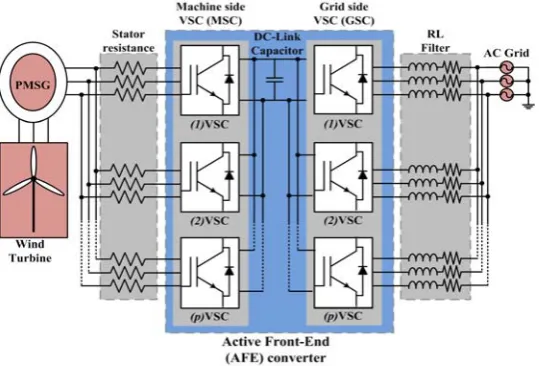
However, its implementation is very difficult, since this must handle very high powers of up to 6 MVA. Notwithstanding, the Active Front-End (AFE) converter topology provides a viable and efficient solution to improve the power transfer capacity and reliability of the WES quality; the AFE converter is generated by modifying a conventional back-to-back converter, from using a single voltage source converter (VSC) to usepVCS connected in parallel, as shown in Figure1. As evidence, in [3] the authors describe the principal WT manufacturers, those in low voltage and medium voltage technologies are classified, generating power ratings of >3 MVA and <3 MVA, respectively. In the open literature there exists some research works that address the AFE converter topology applied to WES; for example, in [17] the authors analytically and experimentally present the control method for the current balance in an AFE power converter of 600 kVA, this is a very important topic in the parallel connection of power converters, however, the authors make the AFE converter analysis connecting only two VSCs in parallel, generating: A THD of 4.32% (three times higher than in our research work with THD of 1.23%); in addition, they use the space vector modulation for the switching of VSCs, which generates a more complex control ifpVSC in parallel are connected.
commerce applications; however, the type‐4 WT with a PMSG (WT‐PMSG) is an attractive and the best option since this is not directly connected to the grid, presenting advantages such as: High efficiency, increased reliability, major variable speed operation, and low cost in maintenance and installation, due the absence of gearboxes [7]. In the type‐4 WT‐PMSG installation the important aspects to prevent are associated problems with the wind‐nature fluctuations. For example: The flicker generation is mainly caused by load flow changes, due to its continuous operation [8]; a power factor not unity, this characteristic happens as the modulation index of the back‐to‐back converter is not high [9]. Voltage sags occur by the sudden changes in the rotor speed of the type‐4 WT‐PMSG and cause a decrement in the transferred power from the dc‐link to the grid [10]. A higher total harmonic distortion (THD) is mainly produced by the power converters switching, this results in serious pulsations in the type‐4 WT‐PMSG output power and in several power losses at the WES [11–12]. All these problems can be mitigated through the full‐scale back‐to‐back converter in the type‐4 WT‐PMSG scheme, and this generates the following advantages [13–16]: (i) Bidirectional power flow; (ii) adjustable dc‐link voltage; (iii) a sinusoidal grid‐side current with an exchange of active and reactive power. These advantages are possible because the generated whole power by the type‐4 WT‐PMSG on the AC grid is supplied through the back‐to‐back converter.
However, its implementation is very difficult, since this must handle very high powers of up to 6 MVA. Notwithstanding, the Active Front‐End (AFE) converter topology provides a viable and efficient solution to improve the power transfer capacity and reliability of the WES quality; the AFE converter is generated by modifying a conventional back‐to‐back converter, from using a single voltage source converter (VSC) to use pVCS connected in parallel, as shown in Figure 1. As evidence, in [3] the authors describe the principal WT manufacturers, those in low voltage and medium voltage technologies are classified, generating power ratings of >3 MVA and <3 MVA, respectively. In the open literature there exists some research works that address the AFE converter topology applied to WES; for example, in [17] the authors analytically and experimentally present the control method for the current balance in an AFE power converter of 600 kVA, this is a very important topic in the parallel connection of power converters, however, the authors make the AFE converter analysis connecting only two VSCs in parallel, generating: A THD of 4.32% (three times higher than in our research work with THD of 1.23%); in addition, they use the space vector modulation for the switching of VSCs, which generates a more complex control if pVSC in parallel are connected.
Figure 1. Type‐4 wind turbine (WT) connected at wind energy system (WES) through the active
front‐end (AFE) converter parallel topology.
The main goal of this work is the AFE converter topology application for the THD reduction in a WES and the increase of power transfer between the WT and the AC grid; generating greater capability, efficiency, and reliability in the energy conversion at the WES.
Figure 1. Type-4 wind turbine (WT) connected at wind energy system (WES) through the active
front-end (AFE) converter parallel topology.
The main goal of this work is the AFE converter topology application for the THD reduction in a WES and the increase of power transfer between the WT and the AC grid; generating greater capability, efficiency, and reliability in the energy conversion at the WES.
[image:2.595.164.434.479.662.2]In this paper, the AFE converter topology applied in the THD reduction at WES is made. Through the AFE converter parallel topology the following advantages were possible:
(i) Increased the converter power capacity.
(ii) Minimized size of each VSC unit, which manages a portion of the total nominal power.
(iii) A reduced ripple on the injected current, which improves the voltage quality at the Point of Common Coupling (PCC).
(iv) An increased equivalent switching frequency, generating a smaller passive filter on the AC-side. (v) The possibility of THD Reduction at the WES, modifying the Digital sinusoidal pulse width
modulation (DSPWM) switching signals in each VSC.
To verify the functionality and robustness of the proposed methodology, an AFE converter formed with three VSCs connected in parallel is incorporated, as shown in Figure1. The WES simulation in Matlab-Simulink®is analyzed, and the experimental laboratory tests using the concept of rapid control prototyping (RCP) and the real-time simulator Opal-RT®is achieved. The obtained results show a WES prototyping that incorporates a type-4 wind turbine with a total output power of 6 MVA and a THD reduction of up to 5.5 times.
This paper is organized as follows: Section2details the modeling of the Type-4 WT-PMSG; first, the modeling power transfer control between the WT-PMSG and AFE converter is generated; subsequently, the modeling of the machine-side VSC control, DC-link control and the grid-side VSC control of the AFE converter is analyzed, and finally, the design of the AFE converter system parameters is presented. Section3presents the modeling of the DSPWM Technique Applied in the THD Reduction. Section4shows the simulated results of a study case for WES. Section5presents the real-time simulation results of a study case for WES using Opal-RT Technologies®. Finally, in Section6, the conclusions are presented.
2. Modeling of the Type-4 WT-PMSG
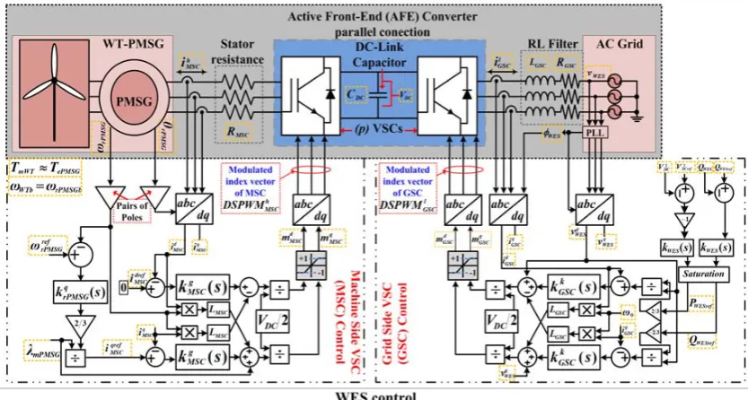
The AFE converter structure consists in two power electronics converters: A machine-side VSC (MSC) to provide power conversion between medium AC voltage and low DC voltage levels, and a grid-side VSC (GSC) to generate the voltages required by the consumers [18], for which, the next sections describe the control modeling of MSC and GSC and these are shown in Figure2.
Energies 2018, 11, 2458 3 of 22
Contributions from this Work
In this paper, the AFE converter topology applied in the THD reduction at WES is made.
Through the AFE converter parallel topology the following advantages were possible:
(i) Increased the converter power capacity.
(ii) Minimized size of each VSC unit, which manages a portion of the total nominal power.
(iii) A reduced ripple on the injected current, which improves the voltage quality at the Point of
Common Coupling (PCC).
(iv) An increased equivalent switching frequency, generating a smaller passive filter on the
AC‐side.
(v) The possibility of THD Reduction at the WES, modifying the Digital sinusoidal pulse width
modulation (DSPWM) switching signals in each VSC.
To verify the functionality and robustness of the proposed methodology, an AFE converter
formed with three VSCs connected in parallel is incorporated, as shown in Figure 1. The WES
simulation in Matlab‐Simulink® is analyzed, and the experimental laboratory tests using the concept
of rapid control prototyping (RCP) and the real‐time simulator Opal‐RT is achieved. The obtained
results show a WES prototyping that incorporates a type‐4 wind turbine with a total output power
of 6 MVA and a THD reduction of up to 5.5 times.
This paper is organized as follows: Section 2 details the modeling of the Type‐4 WT‐PMSG; first,
the modeling power transfer control between the WT‐PMSG and AFE converter is generated;
subsequently, the modeling of the machine‐side VSC control, DC‐link control and the grid‐side VSC
control of the AFE converter is analyzed, and finally, the design of the AFE converter system
parameters is presented. Section 3 presents the modeling of the DSPWM Technique Applied in the
THD Reduction. Section 4 shows the simulated results of a study case for WES. Section 5 presents
the real‐time simulation results of a study case for WES using Opal‐RT Technologies. Finally, in
Section 6, the conclusions are presented.
2. Modeling of the Type‐4 WT‐PMSG
The AFE converter structure consists in two power electronics converters: A machine‐side VSC
(MSC) to provide power conversion between medium AC voltage and low DC voltage levels, and a
grid‐side VSC (GSC) to generate the voltages required by the consumers [18], for which, the next
sections describe the control modeling of MSC and GSC and these are shown in Figure 2.
[image:3.595.89.506.517.740.2]
2.1. Modeling of the Machine-Side VSC Control at AFE Converter
The MSC provides the rotor flux frequency control, thus enabling the rotor shaft frequency to optimally track wind speed [19]. The time-domain relationship of the VSC AC-side is given by:
h
dihMSC(t)/dti=−RhMSC/LhMSChihMSC(t)i+1/LhMSChvhMSC(t)i−1/LhMSChvhWT−PMSG(t)i (1)
wherehis the MSC three-phase vector (a,b,c),LMSCis the PMSG armature inductance,RMSCis the
PMSG stator phase resistance,vMSCandiMSCare the MSC voltage and current, respectively,vWT-PMSG
is the generated WT-PMSG voltage.
Then, the dq reference frame model derived from the AC-side of the MSC, including the inductances cross-coupling, is described as:
d(id
MSC(t)) dt =− Rd MSC Ld MSC h
idMSC(t)i+
ωrPMSGLqMSC Ld
MSC
h
iqMSC(t)i+
vd MSC(t) Ld MSC − vd
WT−PMSG(t) Ld
MSC
(2a)
d(iqMSC(t))
dt
=−
RqMSC LqMSC
h
iqMSC(t)i−
ωrPMSGLd MSC LqMSC
h
id MSC(t)
i −
(λmPMSG)(ωrPMSG) LqMSC
+
vqMSC(t)
LqMSC
−
vqWT−PMSG(t)
LqMSC
(2b)
whereωrPMSGis the PMSG rotor angular velocity;λmPMSGis the maximum flux linkage generated by
the PMSG rotor magnets and transferred to the stator windings. The generated MSC voltage is given by:
h
vgMSC(t)i= (1/2)hmgMSC(t)∗VDC(t)
i
(3)
wheregis thedqcomponents reference frame vector of the MSC,VDCis the DC-link voltage,mgMSCis the modulated index vector.
MakingLMSC=LdMSC =L q
MSC, the presence ofωrPMSGLMSCin (2) indicates the coupled dynamics
betweenid
MSCandi q
MSC. To decouple these dynamics, thei q
MSCvector signals are changed, based in
thedqreference frame, i.e., h
mdMSC(t)i= (2/VDC(t))
h
d
MSC(t)−
(ωrPMSG·LMSC)iqMSC(t)
+vdWT−PMSG(t)i (4a)
h
mqMSC(t)i= (2/VDC(t)) hq
MSC(t) +
(ωrPMSG·LMSC)idMSC(t)
+λmPMSGωrPMSG+vqWT−PMSG(t) i
(4b)
whereEd
MSC(t)andE q
MSC(t)are two additional control inputs.
The MSC plant is obtained by substituting (4) into (3), subsequently, (3) is substituting into (2) generating a first order lineal system that, in Equation (5) is described.
hg
MSC(t)
i
=LMSC
h
digMSC(t)/dti+RMSC
h
igMSC(t)i (5)
Equation (5) in the time domain is represented; its representation in the frequency domain is shown in (6); which describes a decoupled and first-order linear system, controlled throughEgMSC(s).
hg
MSC(s)
i
= (sLMSC+RMSC)
h
igMSC(s)i (6)
Rewriting equation (6), the transfer function representing the MSC plant is given, i.e.,
h
With the purpose of tracking the igMSC(s) reference commands in the loop, the proportional-integral (PI) compensators are used, obtaining:
hg
MSC(s)
i
≈hkgMSC(s)i=
"
(αMSCskpgMSC+αMSCkigMSC)
αMSCs
#
= "
αMSC
s
(skpg
MSC+ki g MSC)
αMSC
!#
(8)
wherekpgMSCandkigMSCare the proportional and integral gains, respectively,αMSC=2.2/τMSCis the
MSC bandwidth of the closed loop control andτMSCis compensator response time.
Substituting Equation (8) into (7), the closed-loop transfer functionhιgMSC(s) i
is formed:
h ιgMSC(s)
i
≈higre fMSC(s)−igMSC(s)i=
αMSC
s
skpgMSC(s)+kigMSC(s)
αMSC
1
sLMSC(s)+RMSC(s)
(9)
If in open loop the expression (9) tends to be∞whens=jω→0 , this guarantees that, in closed loop the system will not have a phase shift delay.
Based on (9), the relation between the plant pole and the PI compensator zero is obtained through (10), generating thekpgMSCandkigMSCcontrol gains.
h
kpgMSCi= [αMSCLMSC] = [(2.2/τMSC)LMSC] (10a)
h
kigMSCi= [αMSCRMSC] = [(2.2/τMSC)RMSC] (10b)
Compensator response time, τMSC, in the range from 5 to 0.5 ms is selected, in this case a
τMSC=2.2 ms is designated.
2.2. Modeling Power Transfer Control between the WT-PMSG and AFE Converter
In the WT-PMSG power transfer modeling the following power-speed characteristics are considered [20]: (i) The base angular velocity of the WT is determined by the base rotor angular velocity of the PMSG,ωWTb =ωrPMSGb; (ii) the WES base power is determined by the WT-PMSG
nominal power,PWESb=PWT-PMSGb;iii) the output base power of the AFE converter is determined by
the base WES power,PAFEb=PWESb; this power is transferred from WT to PMSG through the electric
torque, this is represented by:
[TePMSG] = (3/2)
h
(LdMSC−LqMSC)idMSCiqMSC+ (λmPMSGi q MSC)
i
(11)
whereTePMSGis the PMSG electrical torque,LdMSCandLqMSCare thedqreference frame components of
the PMSG armature inductance.
However, considering that the rotor has a cylindrical geometry, then it is established that, LdMSC=LqMSC[21], generating (12):
[TePMSG] = ((3/2)λmPMSG)
h
iqMSCi (12)
Then, to realize the WT-PMSG variable speed control, it is necessary to generate the plant model that represents it. Therefore, in (13) the dynamic characteristics are shown as a time function so that it represents:
d(ωrPMSG) dt
= 1
Equation (13) analyzes the WT-PMSG in the time domain; however, the WT-PMSG plant representation requires a transfer function to design the ωrPMSG control. By using Laplace
transformation, the WT-PMSG plant in the frequency domain is represented, i.e.,
[ωrPMSG(s)] =
h
(TmWT−TePMSG)(2Hs+D)−1
i
(14)
Equation (14) shows a multiple inputs single output system (MISO); however, because in steady state it is valid thatTmWT≈TePMSG, then, in the control design it is considered thatTmWT= 0; generating
a single input single output system (SISO), as shown in (15).
ωrPMSG(s) −TePMSG
=
1 2Hs+D
(15)
With the purpose of tracking theωrPMSGreference commands in the closed-loop transfer function,
the proportional-integral (PI) compensators are used. The feedback loophιqrPMSG(s) i
is:
h
ιqrPMSG(s) i
=hωrPMSGre f (s)−ωrPMSG(s)
i =
αPMSG
s
(skpqrPMSG+kiqrPMSG)
αPMSG
1 (2Hs+D)
(16)
wherekpqrPMSGandkiqrPMSGare the proportional and integral gains, respectively.
From (16), the relation between the plant pole and PI compensator zero is obtained and the control gains using the next expression are generated:
h
kpqrPMSGi= [2HαPMSG] = [(2.2/τPMSG)2H] (17a)
h
kiqrPMSGi= [αPMSGD] = [(2.2/τPMSG)D] (17b)
where the subscriptτPMSGis the response time by the closed loop of the WT-PMSG first-order transfer
function. This is selected according to the WT-PMSG transferred power and this must be at least ten times higher thanτMSC.
2.3. Modeling of the Grid-Side VSC Control of the AFE Converter
The GSC is used to keep the DC-link constant, transferring the generated power between the WT-PMSG and AC grid. The time-domain relationship of the VSC AC-side is given by:
h
dilGSC(t)/dti=−RlGSC/LlGSChilGSC(t)i+1/LlGSChvlGSC(t)i−1/LlGSChvlWES(t)i (18)
wherelis the VSC three-phase vector (a,b,c),LGSCandRGSCare the RL filter parameters through which
the AFE converter is connected to the grid,vGSCandiGSCare the GSC voltage and current, respectively; vWESis the generated WES voltage.
Then, from (18) the deriveddqmodel is described as:
LGSC
didGSC(t)/dt= (ω0·LGSC)
h
iqGSC(t)i−(RGSC)
h
idGSC(t)i+hvdGSC(t)i−hvdWES(t)i (19a)
LGSC
diqGSC/dt=−(ω0·LGSC)
h
idGSC(t)i−(RGSC)
h
iqGSC(t)i+hvqGSC(t)i−hvqWES(t)i (19b) whereω0is the WES angular frequency; the generated GSC voltages are given by:
vkGSC(t) = (VDC/2)
h
mkGSC(t)i (20)
MakingLGSC = LdGSC = LqGSC, the presence ofω0LGSCin (19) indicates the coupled dynamics
betweenidGSCandiqGSC. Decoupling these dynamics changesmdGSCandmqGSC, based in thedqreference frame, i.e.,
h
mdGSC(t)i= (2/VDC(t))
h
d
GSC(t)−
(ω0·LGSC)iqGSC(t)
+vdWES(t)i (21a)
h
mqGSC(t)i= (2/VDC(t))
hq
GSC(t) +
(ω0·LGSC)idGSC(t)
+vqWES(t)i (21b)
whereEd
GSC(t)andE q
GSC(t)are two additional control inputs.
The GSC plant is obtained by substituting (21) into (20), subsequently, (20) is substituting into (19) generating a first order lineal system, this in Equation (22) is described as:
LGSC
h
dikGSC(t)/dti=hkGSC(t)i−RGSC
h
ikGSC(t)i (22)
The frequency domain of the Equation (22) is shown in (23); which describes a decoupled, first-order, linear system, controlled throughEGSCk (s). Also, Equation (23) represents the grid-side VSC plant.
h
ikGSC(s)i=hkGSC(s)i(sLGSC+RGSC)−1 (23)
With the purpose of tracking the ikGSC(s) reference commands in the closed loop, the proportional-integral (PI) compensators are used, obtaining:
h
k GSC(s)
i
≈hkkGSC(s)i= "
(αGSCskpkGSC+αGSCkikGSC)
αGSCs
#
= "
αGSC
s
(skpk
GSC+kikGSC)
αGSC
!#
(24)
wherekpk
GSCandkikGSCare the proportional and integral gains, respectively.
The feedback loopιkGSC(s)is:
h ιkGSC(s)
i
=hikre fGSC(s)−ikGSC(s)
i =
"
αGSC
s
(skpk
GSC+kikGSC)
αGSC
!
1
sLGSC+RGSC
#
(25)
The relation between the plant pole and the PI compensator zero is obtained in (26), generating thekpkGSCandkikGSCcontrol gains andαGSC=2.2/τGSCis the GSC bandwidth of the closed-loop control.
h
kpkGSCi= [αGSCLGSC] = [(2.2/τGSC)LGSC] (26a)
h
kikGSCi= [αGSCRGSC] = [(2.2/τGSC)RGSC] (26b)
whereτGSCis selected from 5 to 0.5 ms based on the transferred power.
2.4. The DC-Side Control of the AFE Converter
GSC improves the DC-link control. The time-domain relationship of the DC-link of the AFE converter is given by:
[dVDC(t)/dt] = [IDC(t)/CDC]−[VDC(t)/(CDC·RDC)] (27)
The sum of currents entering the capacitor is:
[IDC(t)] =
1 2
c
∑
l=a
The functionality of the AFE converter requires that:
VDC≥ |2(vWESL−L)| (29)
The DC-link control is calculated through the stored energy in the capacitor, that is,
[UDC(s)] = (CDC/2)
h
VDC2 (s)i (30)
whereUDCis the stored energy in the capacitor andCDCis the DC-link capacitance.
Considering thatUDC(s)≈PGSCref(s), and using thedreference frame component of grid-side
VSC plant described in (22) the DC-link control is made, generating the active power control, that is:
h
PGSCre f(s)
i
= (CDC/2)
h
VDCre f2 (s)−VDC2 (s)ihEdGSC(s)i (31)
The reactive power control is made with theqreference frame component of the GSC plant described in (22), that is,
h
QGSCre f(s)
i
=hQWESre f(s)−QWES(s)
ih
d GSC(s)
i
(32)
whereQWESis the presented reactive power at the WES.
It is important to consider that, the subscriptτWESpresented in (32) must be at least ten times
higher thanτGSC.
2.5. System Parameters Design of the AFE Converter
The correct operation of the type-4 WT control depends on the precise design of the AFE converter parameters; thus, the element’s values of the MSC are obtained from the WT-PMSG nominal power, PWT-PMSG, that is: the current isiMSC = (2/3)(PWT-PMSG/vMSC); the machine-side
impedance isZMSCt=vMSC/iMSC, thus, the MSC works with 15% of the total WT-PMSG impedance,
i.e., ZMSC= (0.15)ZMSCt; from the WT-PMSG characteristics the following parameters are taken:LMSC, RMSG, D,H. The element’s values of the GSC are obtained from the WES nominal power, but to
achievePWES=PWT-PMSGiGSCis generated usingiMSC=(2/3)(PWES/vGSC); the grid-side impedance
isZGSCt=vGSC/iGSCthe GSC works with 15% of the total WES impedance, i.e.,: ZGSC=(0.15)ZGSCt;
therefore,LGSCis calculated withLGSC= ZGSC/ω0, theRGSCvalue varies according to the transferred
power, in a range from 0.1 Ω to 0.5 Ω; the base WES capacitance CWES is calculated with CWES= 1/(ZGSCω0). Then, a better time response in the WES feedback is achieved, since theLMSC
andRMSCvalues are used in (10),HandDvalues are used in (17),LGSCandRGSCvalues are used in
(26), to obtain the system feedback gains. It is important to establish that from the generated active power by the GSC,vWESis kept constant in the presence of any perturbation; for which, it is essential
to calculate the correct capacitance value that maintains the DC-link compensation. This is determined from the base DC-link capacitance, i.e.,CDC=(3/8)CWES, determining the store energy in Equation (30).
3. Modeling of the DSPWM Technique Applied in the THD Reduction
Digital modulation techniques are the most generalized framework in the control of modern power electronics converters applications. Digital sinusoidal pulse width modulation (DSPWM) is a modulation technique created by the internal generation of the modulated and carrier signals using a digital controller [22].
signals, generating the DSPWM signal (phase a) corresponding to each VSC connected in parallel. The correct phase shift angle between each carrier signal is established putting up different values of total phase shift angle at the WES, see Figure2. The analysis is shown in Table1.
Energies 2018, 11, 2458 9 of 22
Figure 3 Digital sinusoidal pulse width modulation (DSPWM) signal applied to each voltage source
converter (VSC) connected in parallel (phase a).
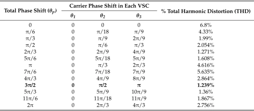
In Table 1 it is observed that the angle that generates a lower THD is 3/2; hence, this angle divides the number of VSCs placed in parallel, i.e.,
(33)
where p is the number of VSC connected in parallel and p is the carrier signal phase shift angle of each VSC.
Table 1. Analysis of different phase shift at the carrier signal.
Total Phase Shift (p) Carrier Phase Shift in Each VSC % Total Harmonic Distortion (THD) 1 2 3
0 0 0 0 6.8%
/6 0 /18 /9 4.33%
/3 0 /9 2/9 1.99%
/2 0 /6 /3 2.054%
2/3 0 2/9 4/9 1.271%
5/6 0 5/18 5/9 1.608%
0 /3 2/3 4.616%
7/6 0 7/18 7/9 5.635%
4/3 0 4/9 8/9 2.864%
3/2 0 /2 1.239%
5/3 0 5/9 10/9 1.36%
11/6 0 11/18 11/9 1.867%
2 0 2/3 4/3 2.756%
The n‐harmonics content is calculated through the Fourier series expansion, i.e.,
(34)
[image:9.595.89.507.569.752.2]where n is the harmonic number, , and . Figure 3.Digital sinusoidal pulse width modulation (DSPWM) signal applied to each voltage source converter (VSC) connected in parallel (phase a).
In Table1it is observed that the angle that generates a lower THD is 3π/2; hence, this angle divides the number of VSCs placed in parallel, i.e.,
θp= (3π/2)/p (33)
wherepis the number of VSC connected in parallel andθpis the carrier signal phase shift angle of
each VSC.
Table 1.Analysis of different phase shift at the carrier signal.
Total Phase Shift (θp)
Carrier Phase Shift in Each VSC
% Total Harmonic Distortion (THD)
θ1 θ2 θ3
0 0 0 0 6.8%
π/6 0 π/18 π/9 4.33%
π/3 0 π/9 2π/9 1.99%
π/2 0 π/6 π/3 2.054%
2π/3 0 2π/9 4π/9 1.271%
5π/6 0 5π/18 5π/9 1.608%
π 0 π/3 2π/3 4.616%
7π/6 0 7π/18 7π/9 5.635%
4π/3 0 4π/9 8π/9 2.864%
3π/2 0 π/2 π 1.239%
5π/3 0 5π/9 10π/9 1.36%
11π/6 0 11π/18 11π/9 1.867%
Then-harmonics content is calculated through the Fourier series expansion, i.e.,
F(t) =C0+ ∞
∑
n=1
CnMSC,GSCcos(nω0t+σ) (34)
where n is the harmonic number, Cn
MSC,GSC =
q (an
MSC,GSC) 2+ (bn
MSC,GSC) 2,
σ=tan−1(bnMSC,GSC/anMSC,GSC)andC0=a0/2.
The magnitude of each harmonic is calculated by,
anMSC,GSC= 2
T
Z T/2
−T/2F
(t)cos(nω0t)dω0t
(35)
bnMSC,GSC=
2 T
Z T/2
−T/2F(t)sin(nω0t)dω0t
(36)
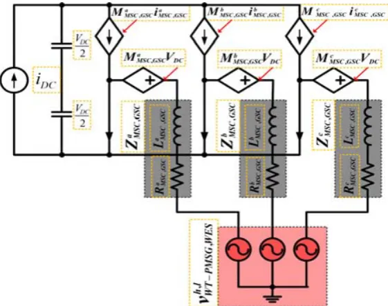
To calculate the THD in the AFE converter, the individually equivalent circuit of each three-phase VSC is analyzed.
A three-phase VSC equivalent circuit is shown in Figure4.
Energies 2018, 11, 2458 10 of 22
The magnitude of each harmonic is calculated by,
(35)
(36)
To
calculate
the
THD
in
the
AFE
converter,
the
individually
equivalent
circuit
of
each
three‐phase VSC is analyzed.
A three‐phase VSC equivalent circuit is shown in Figure 4.
Figure
4
Three‐phase
VSC equivalent circuit.
The three‐phase VSC is represented by the next equation,
(37)
Using Kirchhoffʹs current law (KCL), the currents flowing towards the MSC or/and GSC node
must be equal to the currents leaving the MSC or/and GSC node, i.e.,
(38)
Replacing equation (38) in (37) gives line‐to‐line current of the MSC or/and GSC, i.e.,
(39)
where
v
WT‐PMSGrepresents
the
WT‐PMSG
voltage,
v
WESexemplifies
the
WES
voltage,
v
MSC,GSCis
the
VSC
AC‐side
output
voltage of
MSC or/and
GSC, and
is
the
AC‐side
filter
of
MSC
or/and
GSC.
The
v
MSC,GSCvalue
depends
on
signal
modulation.
The
modulated
and
carrier
signals
implement the DSPWM technique of Figure 3; these have modulation frequencies of 60Hz (
0) and
7kHz (
f
), respectively.
The carrier signal is composed by an up‐slope and a down‐slope, calculated as,
(40)
(41)
where
C
t1,t2pis
the
composed
carrier
signal,
pis
phase
shift
angle
of
each
VSC,
f
is
switching
frequency of the carrier signal,
t
1is the time for the up‐slope,
t
2is the time for the down‐slope.
Figure 4.Three-phase VSC equivalent circuit.
The three-phase VSC is represented by the next equation,
2(Z∗ia) −(Z∗ib) −(Z∗ic)
−(Z∗ia) 2(Z∗ib) −(Z∗ic)
−(Z∗ia) −(Z∗ib) 2(Z∗ic)
MSC,GSC
=
va−vb vb−vc vc−va
MSC,GSC
−
va−vb vb−vc vc−va
WT−PMSG,WES
(37)
Using Kirchhoff’s current law (KCL), the currents flowing towards the MSC or/and GSC node must be equal to the currents leaving the MSC or/and GSC node, i.e.,
[image:10.595.157.438.329.550.2]Replacing equation (38) in (37) gives line-to-line current of the MSC or/and GSC, i.e.,
iabMSC,GSC ibcMSC,GSC icaMSC,GSC
=
1 3ZhMSC,l ,GSC
!
va−vb vb−vc vc−va
WT−PMSG,WES −
va−vb vb−vc vc−va
MSC,GSC
(39)
wherevWT-PMSGrepresents the WT-PMSG voltage,vWES exemplifies the WES voltage,vMSC,GSCis
the VSC AC-side output voltage of MSC or/and GSC, andZhMSC,l ,GSCis the AC-side filter of MSC or/and GSC.
ThevMSC,GSCvalue depends onMhMSC,l ,GSCsignal modulation. The modulated and carrier signals
implement the DSPWM technique of Figure3; these have modulation frequencies of 60Hz (ω0) and
7kHz (fω), respectively.
The carrier signal is composed by an up-slope and a down-slope, calculated as,
Ct1p=1− (4/fω) ω0t1−θp
(40)
Ct2p= (4/fω) ω0t2−(fω/2)−θp
−1 (41)
whereCt1,t2p is the composed carrier signal, θp is phase shift angle of each VSC, fω is switching frequency of the carrier signal,t1is the time for the up-slope,t2is the time for the down-slope.
Timet1for up-slope is:
θp≤t1≤ (fω/2) +θp (42)
Timet2for down-slope is:
(fω/2) +θp≤t2≤ fω+θp (43)
Modulated signals in each VSC are described by the carrier signal time, that is:
Mth,l
1p=cos(t1+ϕ)
Mth,l
2p=cos(t2+ϕ)
(44)
whereh,l = a,b,cthe VSC phases in MSC and GSC, respectively, andϕis the corresponding angle of each phase in the modulated signal.
The comparison between modulated and carrier signals defines the DSPWM signal,
its representation is:
DSPW Mth1,lp=
M
h,l
t1p≤Ct1p
DSPW Mth2,lp=
M
h,l
t2p≤Ct2p
(45)
Multiplying theDSPWMsignal and DC voltage amplitude generates the VSCs output voltage for each phase value in MSC and GSC, i.e.,
vhMSC,l ,GSC=VDC∗DSPW MhMSC,l ,GSC (46)
The WT-PMSG voltagevhWT−PMSGis generated by,
vht
1WT−PMSG=PMSG(cos(ωrPMSGt1+θrPMSG))
vht2WT−PMSG=PMSG(cos(ωrPMSGt2+θrPMSG))
(47)
And the WES voltagevlWESis produced by,
vlt
1WES =WES(cos(ω0t1+φWES))
vlt2WES =WES(cos(ω0t2+φWES))
(48)
whereWESis the AC grid amplitude voltage andφWESis the corresponding angle of each phase in the
three-phase WES grid.
The output current in each VSC is calculated as,
h
iht,l
1MSC,GSC
i
= (1/(3ZMSC,GSC) )
h
vht,l
1WT−PMSG,WES
i
−hvht,l
1MSC,GSC
i
h
iht,l
2MSC,GSC
i
= (1/(3ZMSC,GSC) )
h
vht,l
2WT−PMSG,WES
i
−hvht,l
2MSC,GSC
i (49)
The harmonic content spectrum to obtain the THD is required. By using (35), (36), and (49) the spectrum is calculated as,
an
MSC,GSC= T2
hR(fω/2)+θp
θp
iht,l
1MSC,GSCcos(nω0t1)
dω0t1+Rfω+θp (fω/2)+θp
iht,l
1MSC,GSCcos(nω0t2)
dω0t2i (50)
bnMSC,GSC= 2ThR(fω/2)+θp
θp
ith,l
1MSC,GSCsin(nω0t1)
dω0t1
+Rfω+θp (fω/2)+θp
iht,l
2MSC,GSCsin(nω0t2)
dω0t2 i
(51)
For the harmonic content of the output current signal, the magnitude of the individual harmonics is calculated for each VSC connected in parallel to the MSC and GSC and these are added, i.e.,
anMSC1 ,GSC+anMSC2 ,GSC+. . .+anpMSC,GSC (52)
bnMSC1 ,GSC+bnMSC2 ,GSC+. . .+bnpMSC,GSC (53) wherepis the number of VSCs placed in parallel andnis the number of harmonics.
The THD in the AFE converter output current is,
THDihMSC,l ,GSC= 1
C1MSCp ,GSC
s ∞
∑
n=2
CnpMSC,GSC2
∗100 (54)
whereC1MSCp ,GSCis the fundamental harmonic magnitude andCnpMSC,GSCis thentthharmonic magnitude. Finally, the lower THD content in the output current of the AFE converter is generated when the output current signals of each VSC are added, i.e.,
ihMSC,l ,GSC=ihMSC,l 1,GSC1+ihMSC,l 2,GSC2+. . .+ihMSCp,l ,GSCp (55)
Energies2018,11, 2458 13 of 23
(53)
where p is the number of VSCs placed in parallel and n is the number of harmonics. The THD in the AFE converter output current is,
(54)
where is the fundamental harmonic magnitude and is the ntth harmonic magnitude. Finally, the lower THD content in the output current of the AFE converter is generated when the output current signals of each VSC are added, i.e.,
(55)
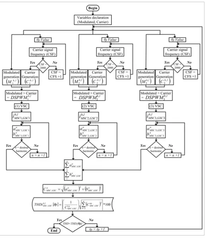
Figure 5 shows the flow diagram that describes the generated method for a lower harmonic content, represented from Equations (33) to (55).
[image:13.595.88.509.88.578.2]
Figure 5 Flow diagram for the lower total harmonic distortion (THD) generation. Figure 5.Flow diagram for the lower total harmonic distortion (THD) generation.
4. Simulation Results: Study Case for WES
In this paper, Matlab-Simulink®(Matlab r2015b, Mathworks, Natick, MA, USA) and Opal-RT Technologies®module (OP-5600) (Montreal, QC, Canada) are the main elements in the WES real-time simulation, since the OP-5600 module uses the rapid control prototyping (RCP) concept, which allows testing of the control law without the need for any programming code.
Energies2018,11, 2458 14 of 23
Table 2.Wind turbine-permanent magnet synchronous generator (WT-PMSG) characteristics.
Wind Turbine (WT)
Nominal output power 2 MW Base wind speed 12 m/s
Pitch angle 45 deg base generator speed 1.2 pu
Permanent Magnet Synchronous Generator (PMSG)
Mechanical input −8.49×10⁵N.m. Stator resistance 8.2×10⁻⁴Ω
Armature inductance 1.6×10⁻³H Flux linkage 5.82
Viscous damping 4.04×10³N.m.s Inertia 2.7×10⁶kg.m2
Pole pairs 4 Rotor type Round
To verify the correct WES operation in Figure2, in Figure6the behavior of the WT mechanical torque and the PMSG electric torque are analyzed.
4. Simulation Results: Study Case for WES
In this paper, Matlab‐Simulink (Matlab r2015b, Mathworks, Natick, MA, USA) and Opal‐RT Technologies module (OP‐5600) (Montreal, QC, Canada) are the main elements in the WES real‐time simulation, since the OP‐5600 module uses the rapid control prototyping (RCP) concept, which allows testing of the control law without the need for any programming code.
In Figure 2, the simulated WES is shown. It contains a WT‐PMSG to supply the MSC, the AFE parallel converter and the infinite bus (considered as an ideal voltage source) to supply the GSC. The MSC and GSC are connected to WT‐PMSG and the AC grid through RL filters, both converters are formed by three VSCs connected in parallel and each one is designed to possess a power and voltage of 2 MVA and 2.5 kV, respectively. The characteristics of the WT‐PMSG are described in Table 2.
Table 2. Wind turbine‐permanent magnet synchronous generator (WT‐PMSG) characteristics. Wind Turbine (WT)
Nominal output power 2 MW Base wind speed 12 m/s Pitch angle 45 deg base generator speed 1.2 pu
Permanent Magnet Synchronous Generator (PMSG)
Mechanical input −8.49 × 10⁵ N.m. Stator resistance 8.2 × 10⁻⁴
Armature inductance 1.6 × 10⁻³ H Flux linkage 5.82
Viscous damping 4.04 × 10³ N.m.s Inertia 2.7 × 10⁶ kg.m2
Pole pairs 4 Rotor type Round
To verify the correct WES operation in Figure 2, in Figure 6 the behavior of the WT mechanical torque and the PMSG electric torque are analyzed.
Figure 6 The behavior of the WT mechanical torque and the permanent magnet synchronous
generator (PMSG) electric torque in the presence of wind fluctuations. (a) Wind fluctuations; (b)
mechanical and electric torque.
[image:14.595.164.430.274.486.2]Figure 6a details the wind fluctuations applied to the WT, which are generated in Matlab‐Simulink by a rotor wind model developed by RISOE National Laboratory based on Kaimal spectra. Figure 6b shows the behavior of the WT mechanical torque and the PMSG electric torque in the presence of wind fluctuations. It is possible to observe that the electric torque follows the mechanical torque behavior, due to the effective structure of the MSC closed‐loop control.
Figure 6.The behavior of the WT mechanical torque and the permanent magnet synchronous generator (PMSG) electric torque in the presence of wind fluctuations. (a) Wind fluctuations; (b) mechanical and electric torque.
Figure 6a details the wind fluctuations applied to the WT, which are generated in
Matlab-Simulink®by a rotor wind model developed by RISOE National Laboratory based on Kaimal spectra. Figure6b shows the behavior of the WT mechanical torque and the PMSG electric torque in the presence of wind fluctuations. It is possible to observe that the electric torque follows the mechanical torque behavior, due to the effective structure of the MSC closed-loop control.
Energies2018,11, 2458 15 of 23
Energies 2018, 11, 2458 14 of 22
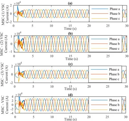
Figure 7 Current present in machine‐side VSC (MSC) of Active Front‐End (AFE) parallel converter.
(a) (1) VSC; (b) (2) VSC; (c) (3) VSC; (d) total current.
Figure 7 shows the generated current by the WT‐PMSG, which is controlled through the MSC of the AFE parallel converter. Because the MSC is formed using the parallel connection of three VSCs, each VSC can handle one third of the total current generated by the WT; Figure 7a–c illustrates the current in the (1), (2), and (3) VSCs, respectively, and in Figure 7d the MSC total current is shown.
While, the main MSC function is the rotor flux frequency control, generating the power conversion between medium AC voltage and low DC voltage levels, the most important GSC function is to keep the DC‐link constant, transferring the generated power between the WT‐PMSG and AC grid in the voltages required by the consumers.
Figure 8a shows that the DC‐link remains constant at 5kV, because, when the MSC requires a reactive power exchange, due to the wind fluctuations of Figure 6a, the GSC restores the DC‐Link, and at the same time injects the needed reactive power, as shown in Figure 8b.
Figure 8 DC‐Link and Reactive Power controlled by the grid‐side VSC (GSC). (a) DC‐link voltage; (b)
exchange of reactive power in WES.
Figure 7.Current present in machine-side VSC (MSC) of Active Front-End (AFE) parallel converter. (a) (1) VSC; (b) (2) VSC; (c) (3) VSC; (d) total current.
While, the main MSC function is the rotor flux frequency control, generating the power conversion between medium AC voltage and low DC voltage levels, the most important GSC function is to keep the DC-link constant, transferring the generated power between the WT-PMSG and AC grid in the voltages required by the consumers.
Figure8a shows that the DC-link remains constant at 5kV, because, when the MSC requires a reactive power exchange, due to the wind fluctuations of Figure6a, the GSC restores the DC-Link, and at the same time injects the needed reactive power, as shown in Figure8b.
Figure 7 Current present in machine‐side VSC (MSC) of Active Front‐End (AFE) parallel converter.
(a) (1) VSC; (b) (2) VSC; (c) (3) VSC; (d) total current.
Figure 7 shows the generated current by the WT‐PMSG, which is controlled through the MSC of the AFE parallel converter. Because the MSC is formed using the parallel connection of three VSCs, each VSC can handle one third of the total current generated by the WT; Figure 7a–c illustrates the current in the (1), (2), and (3) VSCs, respectively, and in Figure 7d the MSC total current is shown.
While, the main MSC function is the rotor flux frequency control, generating the power conversion between medium AC voltage and low DC voltage levels, the most important GSC function is to keep the DC‐link constant, transferring the generated power between the WT‐PMSG and AC grid in the voltages required by the consumers.
Figure 8a shows that the DC‐link remains constant at 5kV, because, when the MSC requires a reactive power exchange, due to the wind fluctuations of Figure 6a, the GSC restores the DC‐Link, and at the same time injects the needed reactive power, as shown in Figure 8b.
Figure 8 DC‐Link and Reactive Power controlled by the grid‐side VSC (GSC). (a) DC‐link voltage; (b)
exchange of reactive power in WES.
Figure 8. DC-Link and Reactive Power controlled by the grid-side VSC (GSC). (a) DC-link voltage; (b) exchange of reactive power in WES.
[image:15.595.171.426.88.327.2] [image:15.595.183.414.479.687.2]Energies2018,11, 2458 16 of 23
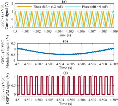
signal does not present any phase shift, generating the DSPWM signal in Figure9c, this is applied to the first VSC connected in parallel in the GSC. In Figure10, the DSPWM generation applied to the second VSC connected in parallel to the GSC is shown; in Figure10a, a phase shift ofπ/2 (rad/s) in the carrier signal is observed. This is compared with the modulated signal of Figure10b, originating the DSPWM with the phase shift of Figure10c. Finally, in Figure11, the DSPWM signal applied to the third VSC connected in parallel of the GSC is presented; in Figure11a the carrier is observed with a phase shift ofπ(rad/s) with respect to the modulated signal of Figure11b, generating the DSPWM of Figure11c.
Figures 9–11 detail the applied DSPWM to each of the VSCs connected in parallel for the correct operation of the GSC, at the stability time from 4.5 to 4.509 ms. In Figure 9, it can be seen that both the carrier signal of Figure 9a and the modulated signal of Figure 9b start at the same time, i.e., the carrier signal does not present any phase shift, generating the DSPWM signal in Figure 9c, this is applied to the first VSC connected in parallel in the GSC. In Figure 10, the DSPWM generation applied to the second VSC connected in parallel to the GSC is shown; in Figure 10a, a phase shift of /2 (rad/s) in the carrier signal is observed. This is compared with the modulated signal of Figure 10b, originating the DSPWM with the phase shift of Figure 10c. Finally, in Figure 11, the DSPWM signal applied to the third VSC connected in parallel of the GSC is presented; in Figure 11a the carrier is observed with a phase shift of (rad/s) with respect to the modulated signal of Figure 11b, generating the DSPWM of Figure 11c.
Figure 9 DSPWM signal applied to the control of the first VSC connected in parallel in GSC. (a)
Carrier signal; (b) modulated signal; (c) DSPWM.
Figure 10. DSPWM signal applied to the control of the second VSC connected in parallel in GSC. (a)
Carrier signal; (b) modulated signal; (c) DSPWM.
Figure 9.DSPWM signal applied to the control of the first VSC connected in parallel in GSC. (a) Carrier signal; (b) modulated signal; (c) DSPWM.
Figures 9–11 detail the applied DSPWM to each of the VSCs connected in parallel for the correct operation of the GSC, at the stability time from 4.5 to 4.509 ms. In Figure 9, it can be seen that both the carrier signal of Figure 9a and the modulated signal of Figure 9b start at the same time, i.e., the carrier signal does not present any phase shift, generating the DSPWM signal in Figure 9c, this is applied to the first VSC connected in parallel in the GSC. In Figure 10, the DSPWM generation applied to the second VSC connected in parallel to the GSC is shown; in Figure 10a, a phase shift of /2 (rad/s) in the carrier signal is observed. This is compared with the modulated signal of Figure 10b, originating the DSPWM with the phase shift of Figure 10c. Finally, in Figure 11, the DSPWM signal applied to the third VSC connected in parallel of the GSC is presented; in Figure 11a the carrier is observed with a phase shift of (rad/s) with respect to the modulated signal of Figure 11b, generating the DSPWM of Figure 11c.
Figure 9 DSPWM signal applied to the control of the first VSC connected in parallel in GSC. (a)
Carrier signal; (b) modulated signal; (c) DSPWM.
Figure 10. DSPWM signal applied to the control of the second VSC connected in parallel in GSC. (a)
Carrier signal; (b) modulated signal; (c) DSPWM.
Figure 10. DSPWM signal applied to the control of the second VSC connected in parallel in GSC.
[image:16.595.180.415.208.420.2] [image:16.595.180.415.463.674.2]Energies 2018, 11, 2458 16 of 22
Figure 11. DSPWM signal applied to the control of the third VSC connected in parallel in GSC. (a)
Carrier signal; (b) modulated signal; (c) DSPWM.
Figure 12 shows the electrical variables present at the GSC when the corresponding phase shift in the carriers of each VSC connected in parallel is performed, according to Equation (33). Figure 12a shows the (1) VSC current generated due to the phase shift at the carrier of Figure 9a; in which, a zoom in time is made from 9.9 to 10.1 s, observing the current magnitude and behavior in the presence of the reactive power exchange at Figure 8b. Figure 12b shows the (2) VSC current generated due the phase shift at the carrier of Figure 10a; Figure 12c shows the (3) VSC current generated due the phase shift at the carrier of Figure 11a; in Figures 12a–c, each current magnitude is 330 A, generating a total GSC current of 990 A, as seen in Figure 12d; Figure 12e details a zoom in time from 9.9 to 10.1 s, observing the generated voltage at the GSC, the magnitude of which corresponds to 2500 V.
Figure12. Electrical variables generated by the GSC. (a) Zoom of the handled current at the (1) VSC;
(b) the handled current at the (2) VSC; (c) the handled current at the (3) VSC; (d) total current; (e)
[image:17.595.181.412.86.281.2]zoom at the magnitude voltage.
Figure 11. DSPWM signal applied to the control of the third VSC connected in parallel in GSC.
(a) Carrier signal; (b) modulated signal; (c) DSPWM.
Figure12shows the electrical variables present at the GSC when the corresponding phase shift in the carriers of each VSC connected in parallel is performed, according to Equation (33). Figure12a shows the (1) VSC current generated due to the phase shift at the carrier of Figure9a; in which, a zoom in time is made from 9.9 to 10.1 s, observing the current magnitude and behavior in the presence of the reactive power exchange at Figure8b. Figure12b shows the (2) VSC current generated due the phase shift at the carrier of Figure10a; Figure12c shows the (3) VSC current generated due the phase shift at the carrier of Figure11a; in Figure12a–c, each current magnitude is 330 A, generating a total GSC current of 990 A, as seen in Figure12d; Figure12e details a zoom in time from 9.9 to 10.1 s, observing the generated voltage at the GSC, the magnitude of which corresponds to 2500 V.
Energies 2018, 11, 2458 16 of 22
Figure 11. DSPWM signal applied to the control of the third VSC connected in parallel in GSC. (a)
Carrier signal; (b) modulated signal; (c) DSPWM.
Figure 12 shows the electrical variables present at the GSC when the corresponding phase shift
in the carriers of each VSC connected in parallel is performed, according to Equation (33). Figure 12a
shows the (1) VSC current generated due to the phase shift at the carrier of Figure 9a; in which, a
zoom in time is made from 9.9 to 10.1 s, observing the current magnitude and behavior in the
presence of the reactive power exchange at Figure 8b. Figure 12b shows the (2) VSC current
generated due the phase shift at the carrier of Figure 10a; Figure 12c shows the (3) VSC current
generated due the phase shift at the carrier of Figure 11a; in Figures 12a–c, each current magnitude is
330 A, generating a total GSC current of 990 A, as seen in Figure 12d; Figure 12e details a zoom in
time from 9.9 to 10.1 s, observing the generated voltage at the GSC, the magnitude of which
corresponds to 2500 V.
Figure12. Electrical variables generated by the GSC. (a) Zoom of the handled current at the (1) VSC;
(b) the handled current at the (2) VSC; (c) the handled current at the (3) VSC; (d) total current; (e)
[image:17.595.185.411.460.721.2]zoom at the magnitude voltage.
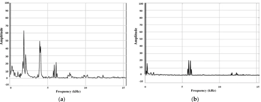
Finally, the current THD is shown in Figure13; Figure13a contents the THD without any phase shift between carriers of each VSC of the AFE converter, which corresponds to 6.8%. Please observe that, in Figure13b, when the corresponding phase shift is performed in the carriers, the current THD is reduced to 1.239%, as specified in Table1. The Figure13shows the harmonics magnitude reduction or even their elimination, once the phase shift between carriers has been made. The THD was reduced by approximately 5.5 times.
Finally, the current THD is shown in Figure 13; Figure 13a contents the THD without any phase
shift between carriers of each VSC of the AFE converter, which corresponds to 6.8%. Please observe
that, in Figure 13b, when the corresponding phase shift is performed in the carriers, the current THD
is reduced to 1.239%, as specified in Table 1. The Figure 13 shows the harmonics magnitude
reduction or even their elimination, once the phase shift between carriers has been made. The THD
was reduced by approximately 5.5 times.
(a) (b)
Figure13. THD present at the WES. (a) Without phase shift between carriers of each VSC; (b) with
phase shift between carriers of each VSC.
5. Real Time Simulation Results: Study Case for WES using Opal‐RT Technologies
To verify the robustness of the applied control in the AFE converter and the THD reduction at
the WES, the grid of Figure 2 in real time using the Opal‐RT Technologies is simulated; generating
an RCP concept that tests the WES dynamics without the need for any programming code.
Specifically, the VSC of the AFE converter is composed by the insulated gate bipolar transistor
(IGBTs), these use a switching frequency of 7 kHz. Figure 14a shows the wind fluctuations generated
by a rotor wind model developed by RISOE National Laboratory based on Kaimal spectra. Figure
14b contains the mechanical torque behavior generated by the wind turbine, and in response to the
applied control at the MSC, the PMSG electric torque is able to follow the same behavior.
Figure 14 Behavior of the WT mechanical torque and the PMSG electric torque in the presence of
wind fluctuations simulated in the Opal‐RT Technologies. (a) Wind fluctuations; (b) Mechanical
[image:18.595.88.509.180.345.2]and Electric torque.
Figure 13.THD present at the WES. (a) Without phase shift between carriers of each VSC; (b) with phase shift between carriers of each VSC.
5. Real Time Simulation Results: Study Case for WES using Opal-RT Technologies®
To verify the robustness of the applied control in the AFE converter and the THD reduction at the WES, the grid of Figure2in real time using the Opal-RT Technologies®is simulated; generating an RCP concept that tests the WES dynamics without the need for any programming code. Specifically, the VSC of the AFE converter is composed by the insulated gate bipolar transistor (IGBTs), these use a switching frequency of 7 kHz. Figure14a shows the wind fluctuations generated by a rotor wind model developed by RISOE National Laboratory based on Kaimal spectra. Figure14b contains the mechanical torque behavior generated by the wind turbine, and in response to the applied control at the MSC, the PMSG electric torque is able to follow the same behavior.
Energies 2018, 11, 2458 17 of 22
Finally, the current THD is shown in Figure 13; Figure 13a contents the THD without any phase
shift between carriers of each VSC of the AFE converter, which corresponds to 6.8%. Please observe
that, in Figure 13b, when the corresponding phase shift is performed in the carriers, the current THD
is reduced to 1.239%, as specified in Table 1. The Figure 13 shows the harmonics magnitude
reduction or even their elimination, once the phase shift between carriers has been made. The THD
was reduced by approximately 5.5 times.
(a) (b)
Figure13. THD present at the WES. (a) Without phase shift between carriers of each VSC; (b) with
phase shift between carriers of each VSC.
5. Real Time Simulation Results: Study Case for WES using Opal‐RT Technologies
To verify the robustness of the applied control in the AFE converter and the THD reduction at
the WES, the grid of Figure 2 in real time using the Opal‐RT Technologies is simulated; generating
an RCP concept that tests the WES dynamics without the need for any programming code.
Specifically, the VSC of the AFE converter is composed by the insulated gate bipolar transistor
(IGBTs), these use a switching frequency of 7 kHz. Figure 14a shows the wind fluctuations generated
by a rotor wind model developed by RISOE National Laboratory based on Kaimal spectra. Figure
14b contains the mechanical torque behavior generated by the wind turbine, and in response to the
applied control at the MSC, the PMSG electric torque is able to follow the same behavior.
Figure 14 Behavior of the WT mechanical torque and the PMSG electric torque in the presence of
wind fluctuations simulated in the Opal‐RT Technologies. (a) Wind fluctuations; (b) Mechanical
and Electric torque.
Figure 14. Behavior of the WT mechanical torque and the PMSG electric torque in the presence of
[image:18.595.162.432.525.718.2]