Int. J. Electrochem. Sci., 7 (2012) 13093 - 13105
International Journal of
ELECTROCHEMICAL
SCIENCE
www.electrochemsci.org
Effect of Thickness on Boron-Doped Silicon Thin Film
Deposited onto Silver-Aluminium Back Contact-Coated Plastic
Substrate by Screen Printing
M. K. M. Ali1*, K. Ibrahim1, E.M. Mkawi1 and A. Salhin2
1
Nano-Optoelectronics Research and Technology Laboratory, School of Physics, Universiti Sains Malaysia, 11800 Penang, Malaysia
2
School of Chemical Sains, Universiti Sains Malaysia, Penang 11800, Malaysia
*
E-mail: hamofarog@yahoo.com
Received: 10 September 2012 / Accepted: 11 November 2012 / Published: 1 December 2012
This paper investigates the effect of thickness on the properties of p-type polycrystalline Si thin film deposited onto silver-aluminium back contact-coated polyethylene terephthalate (PET) substrate. In the fabrication, the substrate was coated using screen printing technology, and boric acid (0.1 g/l) was used as the boron-doping source. Three different weights of boron-doped Si powder were dissolved in 40 ml polyethylene glycol to create Si pastes with different viscosities. These pastes were used to print three different thicknesses of p-type Si thin film on Ag-Al alloy-coated PET substrates. Different techniques were employed to analyze the effects of varying thicknesses on the properties of Si thin layers. X-ray diffraction (XRD) was used to determine the crystallite size (D) and stress in the Si thin film. Surface morphology and roughness were studied by scanning electron microscopy (SEM) and atomic force microscopy (AFM). The thin film component elements were detected using EDX attached to an SEM system. The carrier concentration, Hall mobility, and other electrical properties were determined through Hall Effect measurements. The optical band gap was determined from the UV-visible absorbance spectrum, and the results indicate that band gap energy is proportional to the thickness of the Si layer.
Keywords: (poly-Si) thin film, screen printing; Plastic Substrate; boron; characterization
1. INTRODUCTION
(high efficiency and long-term stability) may be used in many ways given the advantages of thin film technology (large surface areas area, cheap deposition techniques, economical use of semiconductor materials). To reduce costs, Si thin film solar cells on inexpensive foreign substrates have been studied [1-7]. The different methods of growing poly-Si thin films on foreign substrates should aim at large-area grains; such methods include liquid-phase epitaxy (LPE), chemical vapor deposition (CVD) and physical vapor deposition (PVD). These methods enable the fabrication of films with grains (up to ∼100 μm) larger than thin film thickness [8], [9]. When some researchers deposited Si thin films onto substrate-coated seed layers with LPE, uniform and continuous Si thin films with large grains were obtained [3], [9-12]. For Si thin film solar cell applications, the current study investigates the fabrication of Si thin films with different thicknesses on Ag-Al alloy back contact-coated flexible foreign substrates [13].We investigate the crystallization at various thicknesses to determine the optimized process thickness of poly-Si. The influence of thickness on crystallization is reported. The microstructural and electrical properties of poly-Si thin films on PET fabricated by screen printing are investigated. Important factors are suggested for fabricating uniform poly-Si thin films on foreign substrates.
2. EXPERIMENTAL PART
This method used boric acid H3BO3 and silicon powder to obtain boron-doped p-type silicon
using a condensation method. The mixture in the condensation system was stirred at 150 oC by 400 round / min under a nitrogen gas aperture for 4 hours. This procedure was repeated for three constant weights of silicon powder doped with different concentrations of boric acid. The doped silicon powder was dispersed in the paste base, and the viscosity was adjusted by addition of a suitable thinner to the liquid base. Toluene was used as both the original solvent for polyethylene glycol solvent and the thinner. Both the materials and the obtained paste are widely accepted to be non-toxic and environmentally neutral, if not friendly [15].
2.1 Thin Film Preparation:
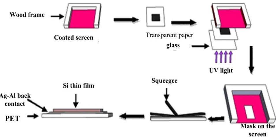
The substrate was a PET sheet, which was ultrasonically degreased in a dilute detergent solution, rinsed in demonized water, and blown dry in N2 gas before use. The PET substrates were coated by a silver-aluminium layer that served as the back contact for the printed Si thin films. Si pastes with three different viscosities and identical doping concentrations were used to print p-type Si films on Ag-Al coated PET substrates. A description of the screen printing process is shown in Fig. 1. The screen was placed a few millimeters above the surface of the PET substrate. Upon loading the Si paste solution onto the screen, a rubber “squeegee” was then swept with a velocity of several centimeters per second across the surface of the screen, momentarily inducing contact with the substrate. At this point, the solution flowed from the screen to the surface of the PET substrate. As the squeegee passed over a region, the screen separated from the substrate, leaving behind a solution that dried to a continuous film. For this study, a 325 mesh silk screen (with 40 × 40 cm2 area), 25 µm emulsion and 45° angle were used for printing the Si paste on the alloy coated with the PET substrate and the mask design detailed in reference [16]
[image:3.596.60.538.489.726.2]
2.2 Thin film characterization
The variation in the viscosity of the Si paste enabled the printing of Si thin films with different thicknesses. .Then, the effect of thickness variation on the properties of the Si thin films was investigated using different techniques. The viscosities were measured by using standard spindles of the Visco Basic Plus viscometer. The thickness of the c-Si film was determined with an optical reflectometer (Filmetric F20). The structural changes in the Si films were evaluated by Raman spectroscopy (Jobin Yvon HR 800 UV). The surface morphology of each Si film was studied by atomic force microscopy (AFM, Ultra Objective) and scanning electron microscopy (SEM, JSM–6460 LV). X-ray diffraction (XRD) measurements were performed using a high resolution X-ray diffractometer system (PANalytical X’ Pert PRO MRD PW3040). Sheet resistance, resistivity, carrier concentration, and Hall mobility were measured using a Hall-effect measurement system (Accent/HL 5500 PC). Using a UV spectrophotometer (U-2000 HITACHI), we measured the optical transmittances of the films as the absorption ratio of a film-coated substrate relative to an uncoated substrate.
3. RESULTS AND DISCUSSION
3.1. Thickness measurement
Many thin film properties are correlated with film thickness. The thickness of the p-type Si films was measured with a surface profile analyzer. The thickness of the screen-printed Si thin film depended on printing parameters, such as the viscosity of the Si paste, the printing angle between the squeegee and screen, and the pressure on the squeegee. The thickness of the thin film increased with increasing Si paste viscosity. In the other films, the thickness of the printed Si thin film decreased with decreasing printing angle and pressure on the squeegee. Three different thickness values (0.81, 2.1, and 12.3 µm) were obtained from Si pastes with the same boron-doping concentration but different viscosities (135, 212, and 319 ma, respectively). The increase in thickness is highly useful for fast and inexpensive fabrication; it also results in a simpler process for the printing of large-area thin films that excellently adheres onto substrate support in a uniform manner. These properties are the advantages offered by the presented technique. It can be easily used directly for device
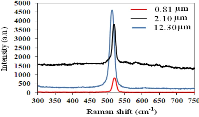
3.2. Raman spectroscopy results
peak positions increased as thickness increased, a result that may be attributed to the strain results, as confirmed by the XRD findings. The Raman instruments dedicated to stress measurements measure frequency changes as small as 0.02 cm–1. For Si, this corresponds to a stress sensitivity of about 10 MPa. Strain or stress and Raman frequency exhibit a complex relationship. All non-zero strain tensor components influence the position of Raman peaks. Nonetheless, in some cases, this relationship becomes simply linear. In general, compressive stress increases Raman frequency, whereas tensile stress decreases it [18], [19].
[image:5.596.187.452.214.392.2]1
Figure 2. Typical Raman spectrum of crystalline silicon powder as starting material
Figure. 3 Typical Raman spectrum of the p-type Si thin films at different thicknesses
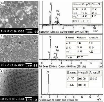
3.3. SEM and DEX Results
[image:5.596.130.464.442.639.2]
morphologies. In Fig 4 (a), different grain sizes of Si were absolved as randomly distributed Wight colour. In Fig 4 (b), the Si film was more homogeneous than that shown in Fig 4 (a) and holes with different sizes, such as porous ones, can be observed. The grain size of the film was larger than that of Fig 4 (a) [20]. Fig 4 (c) is compact, homogenous, and smoother than the Fig 4 (a) and Fig 4 (b) samples. The SEM observations of the crystallized zones show that increasingly larger grains formed with increasing thickness of Si layers. To confirm the presence of p- type Si thin films, the elemental composition of the samples was investigated by energy dispersive X-ray spectroscopy (EDX). Figure 4 shows also a typical result of the EDX measurement of the thin films. Si peaks and other components were detected. Ag and Al can be absorbed because of the back contact alloy. The film in (c) was compact, homogenous, and smoother than those in (a) and (b); hence, the presence of Ag and Al resulted from back contact, which cannot be detected in sample (c)
[image:6.596.121.480.283.636.2]
3.4. Optical properties of Si thin films
The optical absorption spectra of the Si thin film samples were recorded using a UV-VIS double beam spectrophotometer in the range of 300 nm to1100 nm without considering reflection and transmission losses.
Figure 5. A plot of the change in bandgap energy with doping density is shown in the figure below Plot of (αhν)2
of as a function of photon energy p- type Si thin films with different thickness
Fig 5(a) shows the variation in optical absorbance with the thickness of the Si thin films. A plot of (αhν) 2
[image:7.596.171.421.152.645.2](αhν) 2
against hν shown in Fig 5 was determined from the absorption spectra of the Si thin films with different thicknesses t a wavelength range of 300 nm to 1100 nm. The results show that the absorption of Si thin films increased with increasing film thickness, but monotonically decreased with increasing wavelength. The absorption coefficient of the Si thin films was calculated using absorption spectra with the following relation:
(1)
The high value of the optical absorption coefficient (about 104 cm-1) confirms that Si has an indirect band gap. Assuming parabolic bands, the absorption coefficient varies with the energy of radiation [21], [84]:
Si thin films are polycrystalline, and the sizes of the crystallites are proportional to the thickness of the films. Because grain size influences the energy level of electrons, the band gap depends on film thickness. Band gap Eg was calculated using the following relationship (2):
αhυ = A (hν - Eg) n (2)
where α is the absorption coefficient (cm-1); hν is the energy (eV); E
g denotes the band gap
(eV); and n is either1/2 or 2, depending on transition type. n is equal to 1/2 if the transition is direct and allowed; it is equal to 2 if the transition is indirect and allowed. The region where absorption is saturated due to band transition was first identified from the plot of ln (α) against hν. Then, the wavelength range close to the onset of saturation was chosen for curve fitting. Given that the parabolic band approximation holds true only in this region, the optical band gap of the Si in this work was observed between 1.20 and 1.09 eV. These values decreased as thin film thickness increased, which is consistent with the values reported by Prabhune and Fulari. The result may be attributed to the increase in grain size, the decrease in the number of defects, and the changes clearly indicated by the SEM images. The optical spectra show that the absorption and transmission edges shift towards long wavelengths as thickness increased, indicating a decrease in optical band gap Eg [22-24].
3.4. AFM Results
values of the films were found to be 161, 261, and 297 nm for (a), (b), and (c) respectively. The surface roughness significantly changed with increased thickness due to reduced applied pressure on the squeegee via the screen printing mechanism [16].
Figure 6. shows AFM images of p-silicon films deposited on PET substrate (a),(b) and (c) for 0.81 , 2.1 and 12.3 µm respectively
3.5. XRD results
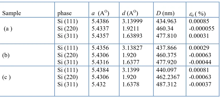
[image:9.596.201.399.130.465.2]
Figure.7 shows XRD images of Ag/Al alloy films deposited on PET substrate (a),(b) and (c) for 900, 750 and 600 nm respectively
Crystal size D of the Si thin films was calculated using the Scherer equation (3) from dominated Si peaks that had the highest intensities at 2= 28.4, 48, and 56 for Si (111), (220), and (313), respectively (3). [24*]ee].
(3)
In this equation, β is the FWHM; k denotes a constant equal to 0.94; and is the incident X-ray wavelength ( = 1.5406 Å) [9]. Lattice parameter a, which is equal to c in this case (cubic), can be calculated from Eq. (2) using the quadratic form of Bragg’s equation. The lattice constant calculated from this pattern was proportional to the thicknesses of the films and consistent with the standard value of ao for bulk Si. The determined lattice constants for three thicknesses reveals that the values of the
lattice parameters increased with increasing thin film thickness. These results are in good agreement with those of Tingting, Song, Yulai, and Gao [25]
The along a-axis and along c-axis) strains, εa and εc, can be calculated from these relations
respectively
where c and a are the calculated lattice parameters. The standard and unstrained parameters values are ao= co = 5.434 AO for Si. The positive values for εa and εc denote tensile strain, whereas the
negative values denote compressive strain. The strain decreased as thickness increased [26], suggesting that crystal quality can be improved by controlling the increase in thickness. The parameter values of lattice parameters a, in-plane strain (εa), and average crystal size determined for the samples are listed
[image:11.596.89.510.238.424.2]in Table 1.
Table 1. Lattice parameters (a = c), in-plane strain (εa), out of plane strain (εc) and average crystal size
determined for the Ag-Al thin films.
Sample phase a (AO
) d (AO
) D (nm) a ( ) (a ) Si (111) Si (220) Si (311) 5.4386 5.4337 5.4357 3.13999 1.9211 1.63893 434.963 460.34 477.810 0.00085 -0.000055 0.00031 (b) Si (111) Si (220) Si (311) 5.4356 5.4306 5.4316 3.13827 1.920 1.6377 437.866 460.375 477.920 0.00029 -0.00063 -0.00044 (c ) Si (111) Si (220) Si (311) 5.4384 5.4306 5.432 3.1399 1.920 1.6378 440.097 462.2367 487.312 0.00081 -0.00063 -0.00037
3.6. Electrical properties of silicon thin films.
The dependence of electrical properties on the thickness is known to be strongly interaction of conduction electrons with the surface. The surface causes the additional scattering of the conduction electrons. This mechanism considerably enhances resistivity provided that the intrinsic scattering length (mean free path Ifree) is of the same order as the film thickness. Resistivity enhancement is
therefore a direct manifestation of fundamental electronic transport parameter Ifree . The dependence of
resistivity on thickness was described by Fuchs within a semi-classical Boltzmann formalism, in contrast to quantum-mechanical theories [27].
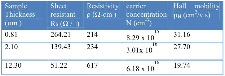
To investigate the electrical properties of poly-Si films, Hall Effect measurements were performed at room temperature. The results indicate that these properties strongly depended on thin film thickness. The best measured values of resistivity ρ, hole concentration p, and Hall mobility μH,p
were achieved from the doped p-type poly-Si with a thickness of 12.1 μm. The low mobility of our samples compared with that (μH,p≈100 cm2/Vs) of mono-crystalline poly-Si at this doping level
size effect. Slater proposed that charge accumulation at grain boundaries influences the energy barrier associated with the grain boundaries and affects barrier height through the increase in this height. The absorption coefficient depended on radiation energy and the composition of the films [30]. A summary of the electrical properties of a typical Si film deposited onto a PET substrate is provided. The electrical properties of poly-Si make it a potentially favorable alternative to poly-Si for P+ gate-material applications in solar cell technologies and thin-film transistor applications.
[image:12.596.117.480.226.349.2].
Table 2. A summary of electrical properties of typical of silicon films deposited on PET substrate
Sample Thickness (µm )
Sheet resistant Rs (Ω /)
Resistivity ρ (Ω-cm )
carrier
concentration N (cm-3)
Hall mobility
H (cm2/v.s)
0.81 264.21 214
8.29 x 10
15
31.16
2.10 139.43 234 3.01x 10¹⁶ 27.70
12.30 51.22 617 6.18 x 10¹⁶ 19.74
4. CONCLUSION
Si thin films of various thicknesses were grown on PET substrates by screen printing. The X-ray and Raman studies reveal the poly-crystalline nature of the films. The SEM and EDX results show different surface morphologies and roughness values. The RMS values increased with increasing thickness. The Hall mobility (μH) of the films was measured through Hall effect measurements. For the
thin films, μH strongly depended on thickness but became independent beyond the bulk value, which
was not reached in this study. In addition, the rate of increase in mobility increased with film thickness. Residual mobility was attributed to overall scattering due to grain boundaries, dislocations, defects, cleavage steps, and other surface effects. Thin film Si obtained from transition has emerged as a viable alternative for the large-scale manufacture of solar cells. The material below the edge has received more attention, and manufacturing plants are currently producing various products using poly-Si technology. Impressive progress has been made in this field and in thin-film Si solar cell applications.
ACKNOWLEDGMENTS
This work was supported by the Nano-optoelectronics Research Laboratory, School of Physics: Universiti Sains Malaysia.
References
2. O .Nast, S. Brehme, D. Neuhaus, S.R Whenham, IEEE Trans. Electron Dev, 46 (10) (1999) 2062 - 2068 .
3. S. Taira, H. Okamoto , PVSEC11 , (1999)189-190.
4. J.H. Werner, R.B. Bergmann, PVSEC-11, (1999) 923-924. 5. A. V. Keitz, J.A.M.V. Roosmalen, G.M. Christie, Thin Film Polycrystalline Silicon Solar
Cells,Seconded. , WCEPV, 1998.
6. G. Andra, J. Bergmann, F. Falk, E. Ose, H. Stafast, Phys. Status Solidi A, 166 (1998) 629-634. 7. B. V.Ehrenwall, A. Braun, H.G. Wagemann , J. Electrical Soc, 147 (1) (2000) 340-344.
8. Z .Shi, M.A .Green, J. Electrochem. Soc, 140 (1993) 3290-3293. 9. J. Kuhnle, R.B .Bergmann, J.H. Wergner, J. Cryst. Growth, 173 (1997) 62-68. 10. S.H. Lee, H.J .Queisser, Mater. Lett, 19 (1994) 1-6.
11. S.H Lee, M.A. Green, J. Korean Association Cryst. Growth, 4 (2) (1994) 119-123. 12. A. Fave, B. Semmache, A .Slaoui , PVSEC-11 (1999) 733-734. 13. O .Nast, A.J .Hartmann, J. Appl. Phys, 88 (2) (2000) 716-724.
14. Stevens , United States Patent. Patent number 5763320. Jun .9, 1998. 15. D. T. Brittonand, M. Härting, Pure Appl. Chem, 78 ( 9) (2006)1723–1739.
16. M. K. M. Ali1 , K. Ibrahim, E.M. Mkawi, M.Z. Pakhuruddin, Advanced Materials Research 364 (2012) 110-114 .
17 . E. I .Scrap, M. Zeman, Kluwer academic publisher group USA.1998. 18. J.A. Sanjurjo, E. L. Cruz, G. Burns, Phys. Rev. B, 28 (12) (1983)7260-7268.
19. F. Cerdeira, W.B. Holzapfel, Phys. Rev. B, 11 (3) (1975) 1188-1192 . 20.H. Kim, G. Lee, D. Kim, S.H. Lee, Current Applied Physics , 2 ( 2) (2002 )129–133.
21.C. Smit, E.A.G. Hamers, B.A. Korevaar, R.A.C.M.M. V. Swaaij, M.C.M. V. Sanden, J. Non-Cryst. Solids, 98 (2002) 299-302.
22. F. I. Ezema, Journ. Univer. Chem. Technol. Metallurgy, 39 (2) (2004)225. 23. F. I. Ezema, Pacific Journ. Sci. Technol, 6 (1) (2005) 6. 24. V. Estrella, M. T. S. Nair, P. K. Nair, Semicond. Sci. Technol, 190 (2003)18.
24. M. Moreno , R. Boubekri, P. R. Cabarrocas, Solar Energy Materials & Solar Cells 100 (2012) 16– 20.
25. Smit. C V. Swaaij, R. A. C. M. M. Donker, H. Kessels, W. M. M.V. Sanden, journal of Apply.Phys,94 (2003) 3582-3588.
26. H. Richter, Z.P. Wang, L. Ley,Solid state communication , 39 (1981) 625-629.
27. G. R. Hastreiter, H. Bruckl, J. Vancea, Physcal Reviw B 43( 6 15) (1991) 5176-5179. 28. R.S. Muller, T. I. Kamins, Device Electronics for Integrated Circuits , second Ed.,Wiley, New
York (1986) 33. 29. H. Kim, G. Lee, D. Kim, S.H. Lee , Current Applied Physics 2 ( 2) (2002) 129–133 . 30.M. Pandlaraman, N. Soundararajan, C. Vijaya, Journal of Ovonic Research 7 (1) (2011) 21 - 27.