Precise measurements of surface resistance of high temperature superconducting thin films using a novel method of Q-factor computations for sapphire dielectric resonators in the transmission mode
244
0
0
Full text
(2) Precise Measurements of Surface Resistance of High Temperature Superconducting Thin Films using a Novel Method of Q-Factor Computations f~r Sapphire Dielectric Resonators in the Transmission Mode. Thesis submitted by Kenneth Tak Ming LEONG BE (Hons) in March 2000. for the degree of Doctor of Philosophy in Electrical and Computer Engineering School of Engineering James Cook University.
(3) 1. Access to Thesis. I, the undersigned, the author of this thesis, understand that James Cook University will make it available for use within the University Library and, by microfilm or other photographic means, allow access to users in other approved libraries. All users consulting this thesis will have to sign the following statement:. "In consulting this thesis I agree not to copy or closely paraphrase. it in whole or in part without the written consent of the author; and to make proper written acknowledgement for any assistance which I have obtained from it.". Beyond this, I do not wish to place any restriction on access to this thesis.. 6fg, I ~ooo. ................ (signature). (date).
(4) ll. Declaration. I declare that this thesis is my own work and has not been submitted in any form for another degree or diploma at any university or other institution of tertiary education. Information derived from the published work of others has been acknowledged in the text and a list of references is given.. 613./:Loro ················· (signature). (date).
(5) iii. Acknowledgements. I wish to convey warmest thanks to my family; Jackson, Roslyn, Helen and Selina, who have given me endless support throughout my studies.. I express sincere thanks to my supervisor A/Prof Janina Mazierska who has provided me tremendous support and guidance.. I also thank Jerzy Krupka of the Institute of Microelectronics and Optoelectronics, Warsaw University of Technology for his expert help and recommendations, as well as A/Prof Greg Allen, A/Prof Keith Kikkert, Dr. Graham Woods of the Department of Electronic and Computer Engineering at James Cook University, Dr. Graeme Sneddon of the Department of Mathematics and Physics at James Cook University, and Patrick Xie of the Texas Center for Superconductivity at the University of Houston.. I wish to thank Dr. Darko Kajfez of the Department of Electrical Engineering at the University of Mississippi for his expert help and encouragement in the early stages of my work on thls thesis.. I also thank all staff of the School of Engineering at James Cook University for their kind help.. Finally, I thank my wonderful friends who were always there for me in support inside and outside the academic environment..
(6) iv. Dedication. This work is dedicated to my parents; Jackson and Roslyn, and my sisters; Helen and Selina..
(7) v. Abstract The work presented in this thesis belongs to the area of microwave characterisation of High Temperature Superconductor (HTS) materials and is devoted to precise measurements of the surface resistance Rs of HTS thin films using the sapphire dielectric resonator structure. Accurate measurements of surface resistance of IITS films are essential for advancement of knowledge and technological progress in the field especially for commercial applications of HTS materials in wireless communications.. In typical measurements of Rs, the superconductor film sample is made an integral part of a microwave resonator, which is a structure that can store microwave energy. The unloaded quality factor Q 0 of the structure measured typically in the transmission mode and is used for calculations of the surface resistance. While there is a need for accurate procedures to measure the surface resistance, no standard procedure has yet been developed for such purpose as no detailed comparative studies were done on the accuracy of existing techniques as well as a lack of superior techniques to determine the unloaded Q0 -factor of microwave resonators working in the transmission mode.. In this thesis, a novel method to accurately and conveniently determine the unloaded Q0 -factor of the transmission mode sapphire resonator for measurements of. Rs of high temperature superconducting thin films is presented. The developed Transmission Mode Q0 -Factor Technique is based on measurements of S-parameters and it accounts for practical effects introduced by a real measurement system which are not always accounted for in simple Q0 -factor techniques. The developed method is applicable not only to the testing of IITS materials using sapphire resonators, but can be successfully employed in any measurements involving transmission mode dielectric resonators..
(8) Contents 1. Introduction 1.1. 1. Major Issues in Measurements of The Surface Resistance of HTS Thin. 4. F~. 2. Review of Superconducting Materials, Phenomena of Superconductivity and Applications of Superconducting Materials. 11. 2.1. Superconductor Materials. 11. 2.2. Physical Phenomena Associated With Superconductivity and Material. 2.3. Parameters of Superconductors. 15. 2.2.1 Vanishing Resistance. 15. 2.2.2 The Meissner Effect. 16. 2.2.3 Zero Dispersion in Superconductor Materials. 17. Relationship Between Transition Temperature, Critical Field, Critical Current and Critical Frequency. 2.4. 2.5. 18. Concept of Resistance and Surface Impedance in Metals and Superconductors. 22. Progress in The Understanding of Superconductivity. 27. 2.5.1 London. Theory. of. Electrodynamics. in. Conventional. 28. Superconductors. 2.5.2 Ginzburg-Landau Theory. 30. 2.5.3 Two Fluid Model. 30. 2.5.4 BCS Theory of Superconductivity. 33. 2.5.5 Progress. in. the. Understanding. of. High. Temperature. Superconductivity. 33. 2.6. Applications of Superconducting Materials. 34. 2.7. Applications of High Temperature Superconductors. 35. 2.7.1 Filters· and Other Systems for Wireless Communications. 37. 2.7.2 Delay Lines for Analog Signal Processing. 40. vi.
(9) Contents. Vll. 2.7.3 HTS Wires and Tapes for Electrical Power Applications, Magnetic Levitational Transport, and High Energy Physics Research. 42. 2.7.4 Josephson Devices for DSP Applications, Detection of Weak Magnetic Fields, Mixers for Wireless Communications, Medical Diagnostics, Digital Electronics and Other Applications 2.7.5 Device Packaging for High Speed Digital Electronics. 3. 43 45. Review of Experimental Techniques Used for Measurements of The Surface Resistance of HTS Thin Films. 49. 3.1. Quality Factor Definition and Energy Transactions in Resonators. 49. 3.2. Equations for Calculations of The Surface Resistance of Superconductor Films Using Loss Equations and Accuracy of Calculations. 51. 3.3. Review of Q-Factor Relationships in Microwave Resonators. 54. 3.4. Resonators. of. Used. for. The. Microwave. Characterisation. Superconducting Films 3.5. 57. Geometrical Factors and EM Field Distribution in Dielectric Resonators 63. 3.6. Determination of the Surface Resistance of HTS Films Using The Sapphire Dielectric Resonator of the Hakki Coleman Type. 3.7. 66. Analysis of Errors in Calculations of Rs of HTS Films Using Ha.k.ki Coleman Resonators Due to Uncertainties in Measurement Parameters 70. 3.8. Unloaded Q0 -factor Measurement Techniques. 72. 3.8.1 Time Domain Techniques for Measurements of Unloaded Q 0 Factor. 74. 3.8.2 Frequency Domain Techniques for Measurements of Unloaded Q0 Factor 3.9. 77. Circle Fitting Procedures Used to Obtain The Unloaded Q0 -Factors of Microwave Resonators From Measurements of S-Parameters. 85. 3.9.1 S21 Phase Technique of Loaded QL-Factor Measurements. 85.
(10) Contents. Vlll. 3.9.2 The S 11 Technique of Loaded Qr.-Factor and Coupling Coefficient ~easurements. 4. 89. Development of a Novel Method for The Accurate Determination of Unloaded Q-Factors of Transmission Mode Dielectric Resonators Based on Measurements of Scattering Parameters and Circle-Fitting 4.1. General Issues to be Considered in the Development of A Hakki Coleman Dielectric Resonator Test System. 4.2. 99 ~odel. of a 99. Practical Effects Introduced by the HTS Microwave Characterisation System. 103. 4.2.1 Assessment of Practical Effects Introduced by a Real ~easurement System to The Transmission and Reflection Responses of the Dielectric Resonator 4.3. Development of A Transmission. 112 ~ode ~ethod. for The Accurate. Determination of The Unloaded Q0 -Factor of Microwave Resonators Based on Measurements of S-Parameters. 4.4. 116. Equations for The Fractional Linear Curve Fitting Procedure to The Transmission Mode Resonator Responses. 5. 128. Assessment of The Accuracy of The Nove] Transmission Mode Q0 -Factor Technique Using Computer Simulations 5.1. 131. Influence of Noise on The Error in The Unloaded Q0 -Factor Obtained From The Transmission ~ode Q0 -Factor Technique. 5.2. 134. Influence of Frequency Dependence of Delay Due to Transmission Lines on Errors in Q0 and a Method to Remove This Effect From Reflection (S 11 or S22) Q-Circles. 5.3 5.4. 140. Influence of The Frequency Dependence of The Coupling Reactance Xs on Errors in Q0 in The Absense of Transmission Line Delay. 147. (~odelled· Using. Rs) on Errors. Influence of Variation in Coupling Losses in Q0 in The Presence of Cable Delay. 151.
(11) ix. Contents. 5.5. Influence of Variation in The Coupling Reactance Xs on Errors in Q0 in The Presence of Cable Delay. 6. 155. Measurements of Surface Resistance of YBa2Cu30, Thin Films Using The Sapphire Resonator and The Transmission Mode Q 0 -Factor Technique Based on S-Parameters. 161. 6.1. Measurement Systems for Rs Testing of HTS Films. 6.2. Measurements of Good Quality YBa2Cu30 7 Thin Films Using a 10 GigaHertz Hakki Coleman Sapphire Resonator. 161. 167. 6.2.1 Measurements of The Unloaded Q0 -Factor Using the Transmission Mode Q0 -Factor Technique Without Phase Correction of Su and S22Traces. 174. 6.2.2 Measurements of The Unloaded Q0 -Factor Under Very Weak Coupling. 175. 6.2.3 Calculations of The Surface Resistance of YBa2Cu3 ~ HTS Films on LaA103 Substrate 6.2.4 Measurements of Poor Quality. 177 YBa2Cu3~. Thin Films Using a 25. GigaHertz Hakki Coleman Sapphire Resonator 6.3. Assessment of The Feasible Range of Q0 -Factor Measurements Using the Transmission Q0 -Factor Technique. 7. 178. 183. Conclusions. 186. 7.1. Future Work and Recommendations. 190. 7.2. Publications Related to Work Presented in This Thesis. 191. A. Equations for The Fractional Linear Curve Fitting Procedure to The Transmission Mode Resonator Responses. 194. B. Implementation of The Fractional Linear Curve Fitting Technique for Fitting to 8 21 -Parameter Q-Circle Data Sets C. Enhanced Phase Correction Procedure. 203 207.
(12) Contents. X. D. Method to Find The Centre and Radius of The Circle Passing Through Data Points Distributed Around a Circular Path Using Linear Least Squares Curve Fitting Technique. 212. E. Fit Results for The 10 GHz Measurements on YBazCu30 7 HTS Thin Films 214 F. Fit Results for The 25 GHz Measurements on YBazCu307 HTS Thin Films 218.
(13) List of Figures Figure 2.1. YBCO structure.. 14. Figure 2.2 Typical temperature dependence of DC resistivity in a superconductor. 16 Figure 2.3 The Meissner effect.. 17. Figure 2.4 The effect of a dispersive medium and a non-dispersive medium on a. Figure 2.5. square pulse passing through.. 18. Superconductor phase diagram.. 19. Figure 2.6 Evolution of transition temperature Tc since the discovery of superconductivity.. 20. Figure 2.7 Critical field versus temperature for Type I superconductors.. 21. Figure 2.8 Critical fields versus temperature for Type II superconductor.. 22. Figure 2.9 Normal wire conductor of length L, cross-sectional area A, with a voltage V. ~pplied. across it's terminals. The wire has a conductivity cr. 23. Figure 2.10 Frequency dependence of surface resistance of copper and YBazCu301-x (YBCO) thin film superconductor around the 800-900 MHz cellular band.. 26. Figure 2.11 Penetration of magnetic field in a superconducting sample.. 29. Figure 2.12 Equivalent circuit for a superconductor modelled on the Two Fluid model.. 32. Figure 2.13 Equivalent circuit for the admittance of a unit cube of superconductor in the Two Fluid model.. 32. Figure 2.14 Possible applications of high temperature superconductors.. 37. Figure 2 .15 Comparison of performance parameters between a high temperature superconducting filter and a conventional normal conducting filter.. 38. Figure 2.16 A 19 pole HTS bandpass filter developed by Conductus Inc. for cellular wireless communications and the insertion loss characteristics of the fllter.. 39. xi.
(14) List of Figures. xii. Figure 2.17 Comparison of system noise figure between a conventional MRC-800 cellular receiver system with the same system fitted with ·a superconducting fllter and low noise amplifier on the front end. Figure 2.18 Superconductive. electronic. applications. of. IITS. in. 39 wireless. communications and digital electronics.. 40. Figure 2.19 A 11 nanosecond delay line made by Dupont. The superconducting line is arranged in a spiral pattern.. 41. Figure 2.20 Block diagram of a monolithic YBCO Josephson mixer circuit mounted in a microwave package.. 44. Figure 3.1 Time dependence of stored energies in a resonator.. 50. Figure 3.2 Microwave losses of a dielectric resonator.. 51. Figure 3.3 Power dissipation in a loaded resonant system consisting of a 54. microwave resonator connected to a external circuit.. Figure 3.4 Power dissipation in a loaded resonant system consisting of a microwave resonator working in the transmission mode.. 56. Figure 3.5 Dielectric resonator fitted with single superconductor film sample.. 58. Figure 3.6 Hakki Coleman type dielectric resonator used in this thesis.. 58. Figure 3.7 Parallel plate resonator.. 59. Figure 3.8 Conventional microstrip resonator.. 60. Figure 3.9 Microstrip resonator in the flip-chip configuration.. 60. Figure 3.10 Stripline resonator.. 61. Figure 3.11 Coplanar wave guide resonator.. 61. Figure 3.12 Confocal resonator.. 62. Figure 3.13 Endplate replacement cavity.. 63. Figure 3.14 Magnetic field distribution (axial Z component) for TEou mode of sapphire resonator with dimensions : Height of the sapphire = 7.41 mm, cavity diameter = 24 mm, sapphire diameter = 12.32 mm, dielectric constant =9.28, Resonant frequency = 10 GHz. Figure 3.15 Electric field distribution (azimuthal cjl component) for the. 65 TEott. mode. of sapphire resonator with dimensions : Height of the sapphire = 7.41.
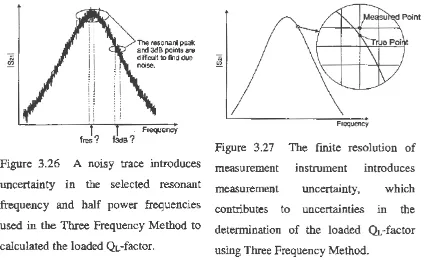
(15) List of Figures. xm. mm, cavity diameter = 24 m.m,. sapphire diameter = 12.32 mm,. dielectric constant= 9.28, Resonant frequency= 10 GHz. Figure 3.16 Losses in Sapphire DR.. 66 67. Figure 3.17 The most probable relative error in Rs versus Rs for various values of uncertainty in unloaded Q0 -factor !lQofQo for a 10 GHz sapphire resonator with assumed uncertainties 11A/A = 0.5%, /lQd/Qd of 1%, lltanB/tanB = 5%; and assumed values Am= 27616, As= 279, Rm = 15 m.Q,. tanB = 5·10·8, Pe = 0.971.. 72. Figure 3.18 Two groups of methods used in detennination of the unloaded Q0 -factor of microwave resonators with typical modes and names of measurements indicated.. 74. Figure 3.19 Time domain Q-Factor measurement system.. 74. Figure 3.20 Time domain determination of Q factor.. 75. Figure 3.21 Power curves measured at the output side, needed to obtain the radiated power Prad(t1) to be used in the calculation of the coupling coefficient on the output side of transmission mode cavity resonator.. 76. Figure 3.22 Reflected power curve measured from the input side, needed to obtain the reflected power Pret{t1) to be used in the calculation of the coupling coefficient on the output side of transmission mode cavity resonator. 76 Figure 3.23 Microwave signals entering and leaving ports for 2-Port microwave resonator.. 78. Figure 3.24 lllustration of measurements of S-parameters on a Two Port microwave resonator.. 79. Figure 3.25 Three Frequency Method used to obtain the loaded QL-factor from the s21. transmission (magnitude) response.. 80. Figure 3.26 A noisy trace introduces uncertainty in the selected resonant frequency and half power frequencies used in the Three Frequency Method to calculated the loaded QL-factor.. 81.
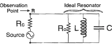
(16) List of Figures Figure 3.27 The. XlV. finite. resolution. of. measurement. instrument. introduces. measurement uncertainty, which contributes to uncertainties in the determination of the loaded QL-factor using Three Frequency Method. 81 Figure 3.28 Distortion in Sz1 trace due to crosstalk.. 84. Figure 3.29 A series RLC circuit of a microwave resonator.. 85. Figure 3.30 Ideal Sz1 Q-circle.. 87. Figure 3.31 Q-circle which has undergone a rotation around the origin due to cable phase shift.. 88. Figure 3.32 Q-circle which has undergone a rotation around the origin due to cable phase shift, followed by a translation due to crosstalk effects.. 88. Figure 3.33 S21 Q-circle with centre at the origin. The phase-frequency dependence of the S21 vector is given by (3.66) to the phase data.. 88. Figure 3.34 Equivalent circuit of the dielectric resonator in the reflection mode.. 90. Figure 3.35 Position of a S 11 Q-circle for a case of lossless coupling, zero coupling reactance, and no delay due to transmission lines.. 91. Figure 3.36 Equivalent circuit to model lossy coupling.. 92. Figure 4.1 A ideal case measurement system used to measure the unloaded Q0 factor of microwave resonators. The input ports of the resonator are accessible.. 99. Figure 4.2 A measurement system used to measure the unloaded Q0 -factor of microwave resonators under low temperature/vacuum conditions. The input ports of the resonator cannot be accessed due to practical constraints.. 100. Figure 4.3 A circuit diagram of a perfect one-port measurement system to measure the unloaded Q0 - factor of microwave resonators.. 100. Figure 4.4 A circuit diagram showing the input port of a practical resonant system to measure the unloaded Q0 -factor of microwave resonators.. 100. Figure 4.5 Component effects of a network connected between the measurement point and the microwave resonator modelled as a cascade of sections. 102.
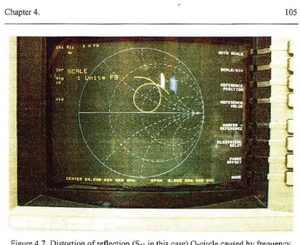
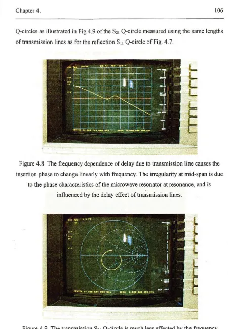
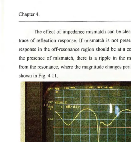
(17) List of Figures. Figure 4.6 The Rs measurement system.. XV. 103. Figure 4.7 Distortion of reflection (Su in this case) Q-circle caused by frequency dependence of transmission line delay.. 105. Figure 4.8 The frequency dependence of delay due to transmission line causes the insertion phase to change linearly with frequency.. 106. Figure 4.9 The transmission S 21 Q-circle is much less effected by the frequency dependence of delay in transmission lines than for reflection (S 11 or S22) circles.. I 06. Figure 4.10 Mismatch effect observed in the off-resonance part of the reflection S22 trace. Figure 4 .11 Mismatch effect observed in the S2z magnitude trace.. 107 108. Figure 4.12 Mismatch effects can cause non-linearities in the phase of the reflection response (Sn or S22).. 109. Figure 4.13 The Szt magriitude trace measured under a relatively weak coupling condition and averaged over 16 sweeps is reasonably well defined.. 110. Figure 4.14 The magnitude-of-S 11 reflection trace is clearly much more noisy than the Sz1 trace of Fig. 4 .13 under the same coupling conditions even after averaging over 16 sweeps.. 110. Figure 4.15 A circuit model of ideal transmission mode resonator system modelled by parallel RLC elements with lossless transmission line connecting to the microwave source and load.. 112. Figure 4.16 illustrative summary of influences of practical effects on S2 1 Q-circles and S21 magnitude trace.. 113. Figure 4 .17 Reflection Q-circles for various cases of coupling loss and coupling reactance.. 114. Figure 4.18 Circuit model of a practical transmission resonator measurement system. 117 Figure 4 .19 Equivalent ~ircuit to model coupling losses.. 123. Figure 4.20 S 11 circle and coupling loss circle in the Smith Chart for the case when observations are made at the input of the resonator.. 125.
(18) List of Figures. XVI. Figure 5.1 Circuit model of the transmission mode dielectric resonator used in the development of the Transmission Mode Q0 -factor Technique.. 131. Figure 5.2 S21. NR=O.OOl equal couplings.. 137. Figure 5.3 Su, NR=0.001 equal couplings.. 137. Figure 5.4 S21. NR=0.002 equal couplings.. 137. Figure 5.5 Su, NR=0.002 equal couplings.. 137. Figure 5.6 S21. NR=0.001 unequal couplings.. 139. Figure 5.7 Su, NR=0.001 unequal couplings.. 139. Figure 5.8 S22, NR=0.001 unequal couplings.. 140. Figure 5.9 Error in Qo using QL of S21 and Sn fits for Qo of 1000.. 143. Figure 5.10 Error in QL obtained from S21 and Sn fits for Q0 of 1000.. 143. Figure 5.11 Error in Qo using Qr. of S21 and Su fits for Q 0 of 10000.. 143. Figure 5.12 Error in QL obtained from S21 and S 11 fits for Q0 of 10000.. 143. Figure 5.13 Error in Q0 using QL of S21 and S11 fits for Q 0 of 100000.. 144. Figure 5.14 Error in QL obtained from S21 and Sn fits for Q0 of 100000.. 144. Figure 5.15 S21 Q-circle for line length= 30A., span= 6.96 MHz.. 145. Figure 5.16 S 11 Q-circle for line length= 30A., span= 6.96 MHz.. 145. Figure 5.17 A 101 point S21 Q-circle subset of the 401 point S21 Q-circle of Fig. 5.15.. 146. Figure 5.18 S21 circle fitted over 401 points of simulated data, with parameters Rst=Rs2=50, Xst=Xs2=20Q, Qo = 1000, IJA=0.55, f0 = 10 GHz.. 146. Figure 5.19 Su circle fitted over 401 points of simulated data, with parameters Rst=Rs2=50, Xst=Xs2=20Q, Qo = 1000, IJA=0.55, fo = 10 GHz.. 146. Figure 5.20 Error in Q0 using QL of S21 and S11 fits for Q0 of 1000 over various values of Xs with dependence on frequency.. 149. Figure 5.21 Error in QL obtained from S21 and Su fits for Qo of 1000 over various values of Xs with dependence on frequency.. 149. Figure 5.22 Error in fitted coupling coefficient obtained for Q0 of 1000 over various values of Xs with dependence on frequency. Equal couplings are used. 149.
(19) List of Figures. XVll. Figure 5.23 Error in Q0 using QL of Szt and Su fits for Q0 of 10000 over various values of Xs with dependence on frequency.. 150. Figure 5.24 Error in Q0 using QL of Szt and Su fits for Q0 of 10000 over various values of Xs with dependence on frequency. Figure 5.25 Error in fitted coupling coefficient for a case of Q0 values of Xs with dependence on frequency.. 150. = 10000 over various 150. Figure 5.26 Error in Q 0 using QL of Szt and Su fits for various Rs and nominal Q0 of 1000. L=0.2A... 153. Figure 5.27 Error in QL obtained from Qr. of Szt and Su fits for various Rs and nominal Q 0 of 1000. L=0.2A... 153. Figure 5.28 Error in coupling coefficient for various Rs and nominal Q0 of 1000. L=0.2A... 153. Figure 5.29 Error in Qo using QL of Szt and S11 fits for various Rs and nominal Q0 of 10000. L--Q.2A... 154. Figure 5.30 Error in QL obtained from Szt and Stt fits for various Rs and nominal Q0 of 10000. L=0.2A... 154. Figure 5.31 Error in coupling coefficient for various Rs and nominal Q0 of 10000. L--0.2A... 154. Figure 5.32 Error in Q 0 using QL of S21 and Sn fits for various X5, nominal Q0 of 1000 and L=0.2A... 157. Figure 5.33 Error in Qr. obtained from Sz1 and S 11 fits for various X5 , nominal Q0 of 1000 and L=0.2A... 157. Figure 5.34 Error in coupling coefficient for various X 5, nominal Q0 of 1000 and L=0.2A... 157. Figure 5.35 Error in Q0 using QL of Szt and Su fits for various X5, nominal Q0 of 10000 and L=0.2A... 158. Figure 5.36 Error in QL obtained from Szt and Stt fits for various X5, nominal Q0 of 10000. L=0:2A... 158. Figure 5.37 Error in coupling coefficient for various X 5, nominal Q0 of 10000 and L=0.2A... 158.
(20) List of Figures. xviii. Figure 6.1 Rs measurement system using the liquid nitrogen bath for refrigeration of the resonator containing the superconductor samples.. 162. Figure 6.2 Rs measurement system using the closed cycle cryocooler for refrigeration of the resonator containing the superconductor samples. 163 Figure 6.3 The 10 GHz Hakki Coleman resonator used in this thesis for measurements of the surface resistance of one inch round wafers of YBa 2Cu 30 7_x HTS thin films.. 164. Figure 6.4 10 GHz Hakki Coleman sapphire resonator with one of the endplates removed, showing the sapphire dielectric puck sitting on top of a superconductor fllm. The coupling loops are inside the cavity for display purposes only.. 164. Figure 6.5 Sapphire resonator inside the vacuum dewar can be seen through the round perspex plate. The cold head which is not visible is below the brass platform.. 166. Figure 6.6 Photo of the main measurement system used in this thesis, showing the HP8722C network analyser, temperature controller, vacuum dewar with the cold head, ffiM-PC computer, and rotary vacuum pump. The compressor of the cryocooler system is not visible in the photo.. 167. Figure 6.7 Measured S21 Q-circle with 1601 points spanning 100kHz and the fitted circle. The fitted QL-factor is 403130, and the fitted resonant frequency f0 is 9.997 GHz.. 168. Figure 6.8 Measured Stt Q-circle with some of the off-resonance trace visible. The · span is 2 :MHz.. 169. Figure 6.9 Measured S22 Q-circle with some of the off-resonance trace visible. The span is 2 MHz.. 169. Figure 6.10 Measured S11 wide-span off-resonance trace (red) shown with the fitted circle. (blue).. The. (0.026963, 0.038702) .. central. coordinates. of. the. circle. are 170.
(21) xix. List of Figures. Figure 6.11 Measured S 22 wide-span off-resonance trace (red) shown with the fitted circle. (blue).. The. central. coordinates. of. the. (0.020116,0.050223).. circle. are 170. Figure 6.12 Phase of S11 plotted with respect to the centre of the off-resonance circle (of Fig. 6.10) verus frequency. A linear fit gives of rate of change in phase of about -3.668 ·10·8 rad/Hz.. 171. Figure 6.13 Phase of S22 plotted with respect to the centre of the off-resonance circle (of Fig. 6.11) versus frequency. A linear fit gives a rate of change in phase of about -4.224 ·10"8 rad!Hz.. 171. Figure 6.14 Corrected S11 Q-circle after phase correction has been applied to the Qcircle of Fig. 6.8.. 172. Figure 6.15 Corrected S 22 Q-circle after phase correction has been applied to the Qcircle of Fig. 6.9.. 172. Figure 6.16 Reduced data set of the corrected S 11 Q-circle of Fig. 6.14, together with the fitted circle.. 173. Figure 6.17 Reduced data set of the corrected S22 Q-circle of Fig. 6.15, together with the fitted circle.. 173. Figure 6.18 A 1601 point S11 Q-circle spanning 120 kHz shown with the fitted circle.. 174. Figure 6.19 A 1601 point S22 Q-circle spanning 120 kHz shown with the fitted circle.. 174. Figure 6.20 A 1601 point S21 Q-circle measured under very weak coupling condition, spanning 100 kHz. The insertion loss at the resonance is about 58 dB. The fitted trace is shown and the fitted QL-factor is 421426. The data scatter Ds is 0.195. Figure 6.21 A 628 point subset from the. S 21. 176. Q-circle of Fig. 6.20 and showing the. fitted circle. The span is 39.187 kHz and the fitted loaded 431634. The data scatter Ds is 0.075.. ~-factor. is. 176.
(22) List of Figures. XX. Figure 6.22 Measured 401 point S21 Q-circle (red) spanning 5 MHz and fitted circle (blue). The fitted loaded QL-factor is 22718 and resonant frequency is 24.75 GHz.. 179. Figure 6.23 Measured S 11 trace over a wide span of 120 MHz centred about the resonance. The S 11 Q-circle is lies within the circular off-resonance trace.. 180. Figure 6.24 Measured S 22 trace over a wide span of 120 MHz centred about the resonance. The S22 Q-circle is lies within the circular off-resonance trace... 180. Figure 6.25 Corrected S 11 circle containing 28 points spanning 8.1 MHz with the fitted trace.. 181. Figure 6.26 Corrected Szz circle containing 18 points spanning 5.1 MHz with the fitted trace.. 181. Figure B 1 The value of S21 at the resonant frequency may not be so accurate for the first curve fitting procedure. Figure C1. 205. Synthesised S11 trace spanning 40 times the loaded bandwidth, showing the distorted S 11 Q-circle and off-resonance curve. The circuit parameters used to generate the trace are : Xst=Xsz=20Q, R1=R2=SQ, Ro=5!l, Q0 =9000, QL=7754, f0 =10GHz, Lt=Lz=70A, N=401 points. 208. Figure C2 Phase of S 11 versus frequency in off-resonance region. Figure C3. S 11 Q-circle after the removal of phase distortion from the S 11 Q-circle ofFig. Cl.. Figure D1. 209 210. N data points distributed about a circular path with the first point (x~. Yt) and last point (xN, YN). The circle has centre {h, k) and radius R which need to be determined.. 212. Figure E 1 Printout results of the linear fractional curve fitting procedure applied to the S21 Q-cifcle with fitted QL of 403130.. 215.
(23) List of Figures. Figure E2. xxi. Printout results of the linear fractional curve fitting procedure applied to the corrected S11 Q-circle showing the real and imaginary parts of the fitted coefficients a1, a2 and a3 .. Figure E3. 216. Printout of the linear fractional curve fitting to the corrected S 22 Q-circle showing the real and imaginary parts of the fitted coefficients a 1, a2 and. a3.. 216. Figure E4 Comparison of the loaded Or--factors, resonant frequencies and Q-circle diameters, and signal-to-noise ratios obtained from S21, Su and S22 fits. 217 Figure E5. Results obtained from the Transmission Mode Q0 -factor Technique showing the computed port coupling coefficients K 1 and K2 of 0.027 and 0.053 respectively, and the unloaded Q0 -factor of 435393 (calculated from Qr_ of S 21 -fit and the port coupling coefficients).. Figure E6. 217. Unloaded Q0 -factor and port coupling coefficients obtained for the case with no phase correction of reflection Q-circles applied. The computed unloaded Q 0 -factor is 434765.. Figure Fl. 218. The loaded QL-factors, resonant frequencies, and signal to noise ratios obtained from the curve fitting procedure applied to the S21 trace, and the corrected S 11 and S22 traces.. 218. Figure F2 Fitted unloaded Q 0 -factor and coupling coefficient results obtained from the full unloaded Q 0 -factor circle fitting procedure.. 219.
(24) List of Tables Table 2.1. Superconducting elements and their transition temperatures.. Table 2.2. Conventional. superconducting. compounds. and. their. 12 transition. temperatures.. 12. Table 2.3. HTS materials and their transition temperatures.. 13. Table 5.1. Errors in unloaded and loaded values of Q-factor, and coupling coefficients under equal couplings in the presence of noise. The computed signal to noise ratio for each noise condition is also given. The noise radius is varied between 0.0005 and 0.02.. Table 5.2. 136. Errors in unloaded and loaded values of Q-factor, and coupling coefficients under different couplings in the presence of noise. The computed signal to noise ratio for each noise condition is also given. The noise radius is varied between 0.0005 and 0.004.. Table 5.3. 139. Maximum error in Q0 obtained from QL of S21 and S 11 fit, and corresponding values of QL and coupling coefficient for Q0 = 1000 for varying transmission line length.. Table 5.4. 142. Maximum error in Q0 obtained from QL of S21 and S 11 fit, and corresponding values of ~ and coupling coefficient for Q0 = 10000 for varying transmission line length.. 143. Table 5.5. Error in Q0 calculated from~ of S21-fit for variations in XJRc.. 149. Table 5.6. Error in QL calculated from~ of Su-fit for variations in XJRc.. 149. Table 5.7. Errors in the unloaded Q0 -factor calculated from the QL-factors of S 21 -fit for variations of RJRc.. Table 5.8. 153. Errors in the unloaded Q0 -factor calculated from the ~-factors of S 11 -fit for variations of RJRc·. Table 5.9. 153. Errors in the unloaded Q0 -factors calculated from QL of S21-fit for variations in XsfRc and Lt =~=0.2A... Table 5.10 Errors in the unloaded Q0 -factors calculated from variations Table 6.1. in XJRc and Lt=~=0.2A... 157 ~. of Su-fit for 157. Results obtained from the Transmission Mode Q0 -Factor Technique showing the loaded. ~-factor. of S21 fit, coupling coefficients, and the. xxii.
(25) List of Tables. xxiii. unloaded Q0 -factor calculated from QL of Sz1-fit and the coupling coefficients. Table 6.2. 174. Surface resistances of YBa2Cu307 on LaAI03 substrate at 9.997 GHz and 77 K calculated from the unloaded Q 0 -factors obtained using three different methods.. Table 6.3. 179. Results obtained from the Transmission Mode Q0 -Factor Technique showing the loaded QL-factor of S21 fit, coupling coefficients and the calculated unloaded Qo-factor calculated from QL of Szt-fit and the coupling coefficients.. 182.
(26) CHAPTER! INTRODUCTION Aims to enhance our society and lifestyles through electronic inventions create needs to improve the performance of electronic devices in various ways such as increase in the operating speed and efficiency, reduced power consumption, and reduced size. Superconductor materials provide opportunities for such improvements to be made. They bring prospects of new technologies as well as hold enormous foreseen potential for commercial applications in a wide range of major industries including wireless communications, remote sensing, digital signal processing, transportation,. and. medicine.. Since the discovery. of high. temperature. superconductivity in 1986 by Bednarz and Mueller, outstanding progress has been made in developments of superconductive products. While attempts to expand on the limited range of industrial applications for superconductors have been unsuccessful even after a few decades of intensive developmental efforts using low temperature superconductors,. the. excellent. results. achieved. with. high. temperature. superconductors over the last ten years look very promising. At present, the most promising applications for superconductors are based on high temperature superconductors in the form of thin ftlms. For applications in high frequency systems, the conventional thin ftlm technology enables realisations of planar HfS devices with superior performances to match conventional state-of-theart. equivalents, with significantly reduced size and weight. Even with incomplete. knowledge of physical mechanisms causing high temperature superconductivity, a plethora of HTS thin film devices and components for wireless communications systems have already been developed. For cellular mobile communications and space communications, which represent the largest future market for high temperature superconductors, a wide range of HTS circuits and components have been built. These include resonators, fllters, mixers, miniature antennas and delay lines. While such circuits are mostly intended for feasibility studies, unambiguous demonstrations of their performance prove that they can be superior to versions made of normal conductors. For example, field trials of prototype consumer HTS filters used in 1.
(27) Chapter 1.. 2. cellular mobile base-stations have been performed in rural areas with impressive results. The results include significantly reduced numbers of dropped calls, significant increase in the area of coverage, and significant increase in the number of satisfied customers using. that corrununications. service. Such convincing. demonstrations of superconductor products have attracted wide publicity and keen interest among prospective customers in the commercial superconductor market of the future, resulting in about 500 HTS filters already installed in cellular base stations in USA. Having introduced some of the significant potential benefits of high temperature superconductors, it should now be mentioned that the excellent progress achieved so far in the HTS field has not been easy. While intensive research and developmental efforts have managed to overcome various major obstacles that had prevented rapid technological progress in superconductive electronics, there are remaining barriers to overcome before the expected benefits of the technology can be acquired. Apart from difficult issues involving the costs and complexities of refrigeration of HTS components, packaging, integration of HTS systems with normal conducting systems, and the fabrication of HTS films, technological progress in the HTS field has been slowed by the incomplete knowledge and control of the behaviour ofHTS fllms. To implement high temperature superconductors effectively, circuit designers need to know the material parameters accurately as well as the characteristics of the material under practical conditions. To obtain accurate parameters and characteristics of HTS films, measurements need to be done as properties of HTS films are very sensitive to fabrication processes [1]. Fabrication processes require precise control of various process parameters to produce HTS films of good quality, such as the temperature, pressure, parameters related to the rate of growth of the film, and parameters related to the control of the stoichiometry. Even small changes in the fabrication process can influence the quality of the film significantly. The electrical characteristics of HTS films are also influenced by the thickness and the type of the supporting substrate, as well as the thickness of the film [2,3]. Furthermore, the.
(28) Chapter 1.. 3. influence of imperfections in the microstructure of the superconductor material on the quality of the film are uncertain until measurements are done to assess it. Due to the above issues, the material parameters of HTS films can only be obtained accurately from measurements of specific films. In the characterisation of HTS films for applications in wireless. communications, the surface resistance is one of the most important parameters to be measured. There is particular interest in the surface resistance for the following three reasons. First, the accurate knowledge of Rs is essential in the design of high frequency superconducting circuits. Secondly, it is used to assess the usefulness of HTS films. Finally, knowledge of the behaviour of Rs in terms of its dependencies on temperature, frequency, and power can aid in the understanding of high temperature superconductivity which is not yet fully understood in terms of the physical mechanisms involved. A better understanding of high temperature superconductivity could ensure the optimisation of fabrication processes to improve the characteristics and quality of superconductors, or perhaps even to customise superconductors to achieve desired physical and electrical properties. Hence there are needs to measure the surface resistance of HTS films accurately. The surface resistance of HTS films is calculated using the unloaded quality factor Q0 of the microwave resonator structure used for the measurement. However, a standard procedure has not yet been developed to measure the unloaded quality factor of microwave resonators used for microwave characterisation of HTS fllms. A International Standards Committee, namely the "International Electrotechnical Commission (IEC) Technical Committee Tc(90) : Superconductivity" [4] has been established for two years with aims to propose a standard structure and measurement devices to be used for measurements of Rs. Reasons for the delay in the development of a standard may be understood in the following introductory background which describes various aspects of surface resistance measurements of IffS films..
(29) Chapter 1.. 1.1. MAJOR. 4. ISSUES. IN MEASUREI\ffiNTS. OF. THE. SURFACE. RESISTANCE OF HTS TlllN FILMS. All measurement systems used to measure the surface resistance Rs of HfS films feature a microwave resonator in which the superconductor sample is mounted, and which serves as a platform for measurements to be made. Measurements are then done to obtain the resonator's unloaded Quality factor which is used in the calculation of Rs via an equation which involves the geometrical constants of the resonator and material constants. Uncertainty in the calculated value of Rs is primarily dependent on uncertainties in the measured unloaded Q0 -factor. Therefore it is important to measure the unloaded Q0 -factor accurately in order to achieve accurate values of surface resistance. The minimisation of errors in Rs also requires :. 1). Accurate knowledge of material constants such as the dielectric loss tangent associated with dielectric losses in the resonator, as well as the surface resistance of normal conducting components in the resonator which account for normal conductor losses.. 2). Accurate values of the geometrical factors of resonator components to be calculated from the knowledge of the resonator geometry and EM field distribution.. Measurements of dielectric loss tangents and of surface resistance of normal conductors also involve measurements of unloaded Q0 -factors of microwave resonators. Hence their accurate measurement are difficult issues in themselves. As for the geometrical factors, they are not easy to obtain accurately for just any kind of a resonator structure (used for measurements of surface resistance of HTS films) as it requires the accurate de:termination of the EM fields in microwave resonator, which can be complicated even for structures with relatively simple geometry. In this thesis, accurate knowledge of the dielectric loss tangent, surface resistance of the normal.
(30) Chapter 1.. 5. conducting parts, and the geometrical factors of the structure are assumed so that the focus of the work is on accurate measurements of the unloaded Q0 -factor. While there are various methods used to measure the unloaded Q0 -factor of microwave resonators, there is no standard procedure. The reason for the lack of a standard procedure is due to the lack of detailed systematic studies of accuracy and reliability of the various existing procedures used, and is also due to a lack of a superior technique to determine the unloaded Q0 -factor of transmission mode microwave resonators which take into account practical effects introduced by a real measurement system. Such practical effects include noise, coupling reactance, coupling loss, electrical delay due to transmission lines, impedance mismatch and crosstalk. Failure to account for the mentioned practical effects contributes toward the uncertainty in the unloaded Q0 -factor obtained from characterisation of the resonator. Hence to measure the unloaded Q0 -factor accurately, it is necessary to account for the practical effects listed above. Unfortunately, this is a very difficult issue particularly when the microwave resonator is confined within a cryogenic or vacuum environment where observations cannot be made at locations as required by idealised Q0 -factor determination techniques. The inability to perform standard device calibration on a microwave resonator due to practical constraints is a main problem to be solved in accurate measurements of the Q0 -factor of microwave resonators. The lack of a standard Q0 - factor procedure also implies the lack of a standard procedure to measure R5• Without a standard Rs measurement procedure, it is difficult to compare results obtained from various measurement laboratories due to the uncertainty in measurement conditions and measurement processing methods used. The development of a standard procedure for the measurement of Rs of HTS films requires consideration of the structure to be used, the types of measurements to be made, and the techniques used to process those measurements to obtain the. unloaded Q0 -factor result needed to calculate R5• The need for a standard technique has already been acknowledged, and steps to develop one is already in progress. A sub-committee, namely Tc-90 of the International Electrotechnical Commission (IEC) has been established for 2 years with aims to propose a standard structure to be used for Rs measurement. So far, a two-resonator system [4] has been proposed.
(31) Chapter 1.. 6. which does not require knowledge of the loss tangent of the resonator that is used in calculations of R 5 • However, the committee has not yet addressed procedures to accurately measure the unloaded Q0 -factor of the resonator. Resonant structures so far used in measurements of Rs of HTS films include the parallel plate resonator, confocal resonator, dielectric resonator, and transmission line resonators. Most of these structures have the potential for accurate measurements of R5 , but not all of them have the same capacity for convenience, reliability, and accuracy in practical situations. Best structures are ones for which analytical solutions for EM fields can be obtained. Also, resonators need to be robust, easy to maintain, and facilitate easy mounting of film samples. Because Hakki-Coleman dielectric resonator structures provide the above desirable qualities, they have become very popular for measurements of Rs of HTS films and make a excellent candidate for the standard device to be used for measurements of the surface resistance [5]. Techniques used to determine the unloaded Q0 -factor of microwave resonators can be divided into time domain and frequency domain techniques and both involve measurements of one or more selected response types around the resonance. For time domain techniques, the unloaded Q0 -factor is obtained by analysing the time-response of the resonator after it has been excited with a pulse of energy from a microwave source. For frequency domain techniques, the unloaded. Q0 -factor is found by processing one of various circuit parameters (impedance, VSWR, microwave power, or S-parameter response) measured around the resonance. Additionally, all Q0 -factor techniques involve the determination of the loaded quality factor. <a. and the port coupling coefficient(s) which are used to calculate the. unloaded Q0 -factor. As Q0 -factor measurement techniques are developed from circuit models of resonator systems, the accuracy of any Q0 -factor technique depends on its ability to account for practical effects which influence the behaviour of the real resonant system. The best technique available so far which takes practical effects into account is the Kajfez method [6,7] to be discussed in detail in Chapter 3.9. The Kajfez method is developed from a full systematic analysis of the losses in a dielectric resonator in the reflection mode and it takes advantage of the circular form of the S-.
(32) Chapter 1.. 7. parameter locus observed at a input port of a microwave resonator around the resonance. However, the method is applicable only to resonators working in the reflection mode and there has been no method of similar quality developed for resonators working in the transmission mode. So far, there has especially been a need for accurate Q0 -factor techniques for transmission mode resonators because measurements of Rs of HTS films and parameters of dielectric materials are typically performed in the transmission mode. Reasons for the popularity of transmission mode resonators for measurements of Rs using dielectric resonators are various. A most obvious one is the relative ease in which the unloaded Q0 -factor can be obtained from transmission measurements using existing transmission mode techniques such as the Three Frequency Method [8], and the Insertion Loss Method [9], even when measurements are done under conditions of very weak coupling. A weak coupling condition can occur when coupling structures (such as coupling loops or probes) of dielectric resonators are placed outside the cavity to prevent disturbance of the nominal EM field distribution in the resonator. A disturbed field distribution is undesirable because Qo-factor measurements are based on a ideal field distribution. For weakly coupled resonators (but not so weak where transmission and reflection mode measurements cannot be made), observations of the S-parameter responses of microwave resonators around the resonance show that the reflection response (Sn or S22) can be significantly influenced by noise while the transmission response (S21) has a much higher signal to noise ratio. For such case described above, it is believed (in my opinion) that the loaded QL-factor of the resonator can be obtained more accurately from transmission mode measurements than from reflection mode measurements of a weakly coupled resonators where the signal-to-noise ratio is much higher in transmission mode measurements than in the reflection mode. For a case of weak coupling, the uncertainty in the unloaded Q0 factor (calculated from the loaded QL-factor and the port coupling coefficients) depends largely on the uncertainty in loaded ~-factor. For dielectric resonator cavities fitted with coupling loops, there are cases where the reflection response is too weak and noisy to provide any reliable measurements of the Q0 -factor for any position of the coupling structure outside the.
(33) Chapter 1.. 8. cavity while the transmission response can still be measured reliably. Under such circumstances described, it is advantageous to use transmission mode measurements for characterisation of HTS films. Also, for high power measurements of the surface resistance of HTS fllms where a amplifier is inserted between the measurement instrument and the resonator, measurements of the reflection response of the resonant system can be impeded by the amplifier. For such a case it is advantageous to use a transmission mode resonator because transmission measurements can still be performed. All of the issues discussed above contribute towards the popularity of transmission resonators for measurements of surface resistance of superconducting materials. From the knowledge obtained from literature and discussions with scientists and engineers working in the HTS field, the author has identified a need for accurate measurements of the unloaded Q 0 -factor of transmission mode resonators via measurements of S-pararneters when taking into consideration practical effects introduced by a real measurement system, such as noise, crosstalk, transmission line delay, coupling losses, coupling reactance, and impedance mismatch. Hence, the aim of this thesis was to develop a accurate transmission mode technique based on the above considerations and issues. The format of the thesis is as follows : Chapter Two. of this. thesis. is. devoted. to the phenomenon. of. superconductivity. The goals of this chapter are to provide a reader with specific knowledge of various aspects of superconductivity, namely material properties, overview of physics of superconductors, and basic applications of superconducting materials. Chapter Three discusses experimental techniques used for measurements of surface resistance of HTS films. The chapter begins with a general description of basic measurement principles followed by defmitions of the Quality factor; a general procedure to calculate the surface resistance of HTS films from a loss equation; relationships between the unloaded Q0 -factor of an isolated resonator and the loaded QL-factor; and a review of microwave resonator structures used in measurements of R 5 • Also included in the chapter is a review of Q0 -factor measurement techniques, with comments on their advantages and deficiencies; and discussion on uncertainties in Rs calculations..
(34) 9. Chapter 1.. In Chapter Four, a new method for accurate measurements of the unloaded Q0 -factor of transmission mode dielectric resonators developed in the course of this. work is presented. The procedure is based on measurements of all three S-parameter modes (S21, S 11 and S22) around the resonance and features a accurate curve fitting technique. The method takes into account important practical and parasitic effects introduced by the measurement environment which include noise, cross-talk, effects of connecting cables such as cable loss and delay; coupling losses, and coupling reactance. Chapter Five presents assessments of the developed transmission mode unloaded Q0 -factor determination technique using computer simulations. The assessment is based on studies of the accuracy in the unloaded Q0 -factor obtained from the application of the technique to simulated data in the presence of practical effects such as electrical delay due to cables connected between the measurement device and the test resonator, coupling reactance, and coupling loss. The study proved that the developed technique can provide accurate Q0 -factor results with less than 1 percent error. In Chapter Six, measurements of the surface resistance of. YBa2Cu 3 ~. HTS. thin films using Hakki Coleman sapphire resonators at 10 GHz and 25 GHz and the developed Transmission Mode Q0 -Factor Technique are presented to verify the accuracy and usefulness of the technique. The conclusions to the thesis are presented in Chapter Seven, which includes a discussion on the achievements made in the course of this thesis, future work to be done and a list of publications related to the work presented in this thesis..
(35) BffiLIOGRAPHY OF CHAPTER 1. [1] R. Humphreys, "Growth and processing of HTS thin films", NATO Advanced Study Institute Microwave Superconductivity, 1999. [2] J. Ceremuga, J. Krupka, R. Geyer, J. Modelski, "Influence of film thickness and air. gaps. on. surface. impedance measurements. of high. temperature. superconductors using the dielectric resonator technique", IEICE Trans. Electronics, Vol. E78-C, No. 8, pp. 1106-1110, 1995. [3] P. Hartemann, "Effective and intrinsic surface impedances of high-Tc superconducting thin films", IEEE Trans. Appl. Supercond., Vol. 2, No. 4, pp. 228-235, Dec 1992. [4] "Superconductivity:. Measurement. Method. of Surface. Resistance. of. Superconductors at Microwave Frequencies", International Electrotechnical Commission (IEC) Technical Committee Tc(90): Working Group 7. [5] J. Mazierska, "Dielectric resonators as a possible standard for characterisation of high temperature superconducting films for microwave applications", Journal of Superconductivity, VoL 10, No.2, pp. 73-85, 1997. [6] D. Kajfez, "Q Factor", Vector Fields, 1994. [7] D. Kajfez: "Linear fractional curve fitting for measurement of high Q factors", IEEE Trans. Microwave Theory Tech., Vol. 42, No.7, pp. 1149-1153, 1994. [8] D. Kajfez, P.Guillon, "Dielectric Resonators", Vector Fields, 1990. [9] D. Kajfez et al, "Uncertainty analysis of the transmission-type measurement of Q-factor", IEEE Trans. Appl. Supercond., VoL 47, No. 3, pp. 367-371, Mar 1999.. 10.
(36) CHAPTER2. REVIEW OF SUPERCONDUCTING MATERIALS, PHENOMENA OF SUPERCONDUCTIVITY AND APPLICATIONS OF SUPERCONDUCTING MATERIALS. From earliest observations of superconductors, superconductivity manifested itself in the remarkable disappearance of electrical resistance at reduced temperatures. Materials of such nature were accordingly named superconductors although the proper classification of superconductors involve a number of other exotic behaviours. The ability of a superconductor to carry current without resistance creates numerous possibilities for electronic applications. Electrical power passing through a resistance-free medium is not lost in the form of heat. It means that electrical devices and components made out of resistance-less conductors could be made very efficient, and high efficiency is very beneficial to the performance of electronic systems. Other ·properties of superconducting materials include zero dispersion and diamagnetism, which also provide vast possibilities for electronic applications. Hence much work is being done to develop superconducting materials of enhanced properties for commercial applications.. 2.1. SUPERCONDUCTOR MATERIALS. Superconductor materials have been classified into two categories depending on their transition temperatures, namely the conventional low temperature superconductors (LTS) and the high temperature superconductors (HTS). While the physics of superconductors is discussed later in this chapter, it is useful to mention at this point that the underlying mechanisms responsible for superconductivity in the two classes of materials are not alike. Conventional superconductors are found to exist in both organic and nonorganic forms. Organic superconductors include fullerenes doped with alkali metals such as. K3~. and Rb3C;o, but so far they have no electronic applications. The non-. organic group, which include a host of simple elements, alloys and polymers have potential for electronic applications. A list of conventional superconductor elements 11.
(37) Chapter 2.. 12. and compounds, and their transition temperatures T c are presented respectively in Table 2.1 and Table 2.2 [1]. The temperature of a superconductor needs to be below its transition temperature in order to exhibit superconducting phenomena, provided that other critical values, namely the operating frequency, current and magnetic field are not exceeded. Mercury, with a Tc of about 4.2K was the first superconductor discovered by Onnes in 1911 [1]. As far as it is known, the element tungsten has the lowest transition temperature with Tc of 0.012 K. A niobium compound (Nb3Ge) discovered in 1973 has the highest T c (about 22.3 K) of the conventional superconductors.. Table 2.1 Superconducting elements. Table 2.2 Conventional superconducting. and their transition temperatures [ 1].. compounds and their transition. Mo. Tc(l() 1.196: 0.56 1.091 0.09 4.15 3.95 3.40 0.14 4.9 6.06 0.92. Nb Os. 9.26 ' 0.655_. Element AI Cd. Ga Hf a.-Hg ~-Hg. In Ir a.-La. 13-La. Element Pa Pb Re Ru Sn Ta Tc Th. v w Zn Zr. Tc{I() 1.4 7.19 1.698 0.49 3.72 4.48 7.77 1.368 5.30 0.012 0.875 0.65. temperatures [ 1]. Compound Nb3 Sn Nb3Ge NbN NbO BaPb0.75Bio.2S03. UBeJ 3 Pb0.7Bio.3 (SN), (BEDT)2Cu(NCS1. 'f.:(K) 18.05 22.3 16 1.2. 11 0.75 8.45 0.26 10. High temperature superconductors were discovered in 1986 when Bednorz and Mueller detected superconductivity in the cuprate La-Ba-Cu-0 (with Tc up to 40K). Their discovery was unexpected because the transition temperature of La-Ba-. Cu-0 far exceeded those of superconductors known at that time [1,2]. While the physical nature of high temperature superconductivity is still not fully understood, a great deal is now known about the chemistry and physical characteristics of high temperature superconductors. All high temperature superconductors discovered so far are cuprates (copper oxide compounds) with structures based on perovskite cells..
(38) Chapter2.. 13. Their transition temperatures are significantly higher than those of conventional superconductors. As they are ceramic materials, high Tc cuprates have hard and brittle textural characteristics. A range of high Tc cuprates are listed in Table 2.3 [3], which includes three most popular HTS materials for electronic applications, namely YBa2Cu3(h (YBCO, Tc=93K for bulk material), Bh(Sr2Ca)Cu20 s (BSCCO, Tc=110K), and ThBa2Ca2Cu03010 (TBCCO, Tc=125K).. Table 2.3 HTS materials and their transition temperatures [3].. Class. HTS Compounds. Tc {K). Notation. Cuprates. (La,Ba)2Cu04-x. 38. La-0201. (La,Sr,Ca)3Cu206±x. 60. La-0212. YBa2CU3(h. 92. Y-123. YBa2Cu40s. 80. Y-124. Y2B~Cu101s. 40. Y-247. BhSr2CaCu20 s. 90. Bi-2212. BhSr2Ca2Cu301o. 110. Bi-2223. CuBa2CaCu30s. 125. Cu-1234. CuBa2Ca3Cu401o. 120. Cu-1223. (Sr,Ca)4Cu30s. 90. 0223. (Sr,Ca)sCu40IO. 80. 0234. ThBa2CaCu20s. 110. Tl-2212. ThBa2Ca3~012. 121. Tl-2234. TlBa2CaCu2~. 100. Tl-1212. TlBa2Ca2Cu309. 123. Tl-1223. T1Ba2Ca3Cu4011. 122. Tl-1234. TJBa2Ca2Cu3010. 127. Tl-1223. ThBa2Cu06. 95. Tl-221. ThBa2Ca3Ct4012. 112. Tl-2234. Hg Ba2Ca2Cu30s. 134. Hg-1223. I. !. i I. I.
(39) Chapter 2.. 14. Hg BazCazCu30s. 164(under pressure). Hg-1223. Hg BazCu304+x. 95. Hg-1201. Hg BazCazCuz06+x. 125. Hg-125. Hg BazCa3Cu401o. 130. Hg-1234. PbzYSrzCu30s. 70. Pb-2123. (Pb,Cu)(Sr,La)zCuOs. 53. PbCu-1212. PbBaSrYCu30s. 50. Pb-2212. I. I. -·-·-. I. I. -. Structurally, a high Tc cuprate is typically made up of a layered arrangement of Cu-0 planes with oxygen layers or rare earth layers in between as illustrated for the YBCO compound in Fig. 2.1 [1,4]. The CuO planes (a-b plane) are considered to be the active superconducting layers while the other layers serve to chemically stabilize. the structure and to dope the CuO planes. Since conduction is generally along the a-b plane, HTS cuprates are grown with the c-axis perpendicular to the substrate layer. Material properties of high Tc cuprates depend strongly on the stoichiometry so that a high T c material is achieved only for particular levels of doping. Depending on the doping, a material can be either metallic, insulating, superconducting, antiferromagnetic or a spin glass [5,6].. • Cu(1) In Chains o Cu(2) In CuO Planes. ~~a 0 0. Figure 2.1 YBCO structure [1,4]..
(40) Chapter2.. 2.2. PHYSICAL. 15. PHENOMENA. ASSOCIATED. WITH. SUPERCONDUCTIVITY AND MATERIAL PARAMETERS OF SUPERCONDUCTORS Superconducting materials have three fundamental phenomena associated with them, which include the vanishing resistance phenomenon, diamagnetic behaviour, and zero dispersion property. In this section, aspects of these phenomena are discussed.. 2.2.1 VANISHING RESISTANCE According to the classical theory of superconductivity, the DC resistivity of a superconductor is zero at temperatures below its transition temperature T c· That is, when a constant, time-independent EM field is applied to a superconducting material at a temperature below the transition temperature, it will exhibit no resistance to current flow and no power will be dissipated in the material. While absolute zero temperature has never been achieved, the DC resistivity of a superconductor has been measured (by measuring over a long period of time the magnetic field associated with a induced current that flowed around a superconducting coil after the source had been removed) with the most sensitive equipment to be less than. w-27 Q-. cm for temperatures well below the transition temperature. Such a value is considered insignificant and it strongly supports the theoretical predictions of a zero DC resistance [ 1]. The DC resistivity of a superconductor has a temperature dependence as shown in Fig 2.2. At temperatures above the transition temperature, the material is in the normal state and therefore exhibits it's normal resistivity. As the temperature is reduced gradually, the resistance also decreases gradually with the temperature until Tc is reached, where the resistance drops abruptly to zero..
(41) Chapter 2.. 16 350. -. 300. E 250. ~. -~ 200. >. :;; 150 c;;. al 0:::. 100 50 1---:i. 0. '. 0. 50. 100. 150. 200. 250. Temperature (K). Figure 2.2 Typical temperature dependence of DC resistivity in a superconductor [7].. In the presence of a time varying field, the resistance of a superconductor is non-zero, although the magnitude of its resistance is much lower than in best conventional conductors over a wide range of frequencies. In the microwave frequency range, where ·some of the most promising applications for superconductors exist, the typical resistance of a superconductor is lower than in the best normal conductors by a few orders of magnitude.. 2.2.2 THE MEISSNER EFFECT The Meissner effect (discovered in 1933 by Meissner and Ochsenfeld) describes the diamagnetic behaviour of superconducting materials and expulsion of magnetic fields [1]. When a constant, time-independent magnetic field is applied to a superconducting material, it causes induced currents to be set up in the surface region of a superconductor. These currents flow in rings and are referred to as screening currents to distinguish them from transport currents. The applied magnetic field is opposed by the magnetic fields associated with the screening currents, which results in the diamagnetic behaviour of superconductors known as the Meissner as illustrated in Fig. 2.3..
(42) Chapter 2.. 17. T> Tc. T< Tc. Figure 2.3 The Meissner effect. Magnetic fields penetrate into the superconductor when it is in the normal state, but the field is repelled when the material is in the superconducting state [1].. The magnetic fields. are not completely screened out from. the. superconductor, and they actually penetrate a small distance into the material. The penetration distance is very small because the strength of the field decays exponentially with distance from the surface. The depth at which the field falls to 1/e of the field at the surface is called the London penetration depth, or simply the penetration depth [1,2,8]. In relation to the distribution of currents in the material, transport currents flowing in superconducting material are confined mostly to the region bounded by the surface of the superconductor down to the penetration depth. In tl}is respect, the penetration depth is comparable to the skin depth (due to the skin. effect) of normal metals, except that the penetration depth has no frequency dependence, but has a temperature dependence.. 2.2.3 ZERO DISPERSION IN SUPERCONDUCTOR MATERIALS Superconductors have a zero dispersion property [9]. It means that frequency components in a composite signal can travel through superconducting materials at the same velocity. For practical purposes, dispersion-free conductors would be very beneficial to pulse type electronic applications, namely digital and analog signal processing. The benefits of dispersion-free media can be understood by considering a square pulse that travels through a transmission line. If the line is dispersive, the.
(43) Chapter2.. 18. result is a distortion of the pulse in the time domain due to the frequency dependence of the phase velocity of frequency components in the signal [10]. The effect of dispersion is recognised by a rounding of the edges of the pulse as illustrated in Fig. 2.4 [11]. Such distortion is undesirable in signal processing applications where detection of the pulse edges are important. At high clock speeds where pulses are very narrow and closely spaced in time, the effects of dispersion become a limiting factor in the speed of pulse applications [12]. If the transmission line is a nondispersive one, then the shape of the pulse is preserved (Fig. 2.4). While practical superconducting transmission lines exhibit some dispersion due to the influence of the supporting structures such as dielectric substrates, the level of dispersion is considered to be negligible for the current frequency ranges of interest for electronic applications, such as below 150 GHz [1].. Pulse In. _Il:J. Pulse Out (Distorted). I. Dispersive Medium. Je. tPulse In. _Il:J .Superconductor. Pulse Out (Preserved). :~· -l. Jl-. Figure 2.4 The effect of a dispersive medium and a non-dispersive medium on a square pulse passing through [11].. 2.3. RELATIONSHIP CRITICAL. BETWEEN. FIELD,. TRANSITION. CRITICAL. CURRENT. TEMPERATURE, AND. CRITICAL. FREQUENCY In order to exhibit superconducting phenomena, a superconductor must. operate below threshold values of temperature, applied magnetic field, current, and frequency, which are known respectively as the transition (critical) temperature Tc, critical field He. critical current Jc and critical frequency..
(44) Chapter2.. 19. The critical frequency of a superconductor is in the order of 100 GHz for low temperature superconductors [8], which is in the optical range. At these frequencies, the photons of electromagnetic waves excite superconducting electrons with enough energy to drive them to the normal state. But as electronic applications for superconductor materials are mainly aimed for frequencies well below 100 GHz, the critical frequency is not so important. The interdependence of Tc.. He and lc is. illustrated in the phase diagram (Fig. 2.5) which shows the transitional boundary between the superconducting phase and the normal phase of a superconductor.. Current density. J. Normal. Figure 2.5 Superconductor phase diagram [13].. The transition temperature (also referred to as the critical temperature) is the highest temperature at which a material can exist in the superconducting state. For practical applications of superconductivity, it is desirable to operate at the highest possible temperature to minimise the overheads of cryogenic refrigeration, and also to minimise the stresses on device components during temperature cycling. Superconductors with transition temperatures as high as 162 K have been found [ 14], and materials with even higher transition temperatures are still being sought. Fig. 2.6 illustrates the evolution of transition temperatures since the discovery superconductivity.. of.
(45) 20. Chapter2. Hg-Ba-ca-cu-0 1993 (150) +Jul 1988 (162) (under pressure) Th-Ba-Ca-cu-0 1 Mar 1988 (103, 125) 100 r Feb 16, 1987 Y-Ba-Cu-0 . (95) 90. f. 80 ~ Jan 8, 1987. 70 60. Jan 1987 (under pressure) Dec 1986. gt-v 50 La-Sr-cu-o. 40. t Dec 1986 Apr1986. 30 20. Uquid Ne Nb,Ge Nb SNb-AI-Ge ~ NbN s n ,..........=! I La-Ba-cu-o NbO . j Jan. 27, 1986. Uquid H2. =- -·. 10. 0. 1986. ..... 1930. 1950. 1970. 1990. Figure 2.6 Evolution of transition temperature T c since the discovery of superconductivity [15].. The critical field for a superconductor is defined as the highest value of external magnetic field strength applied to a superconductor without causing superconductivity to be destroyed, although there is a variation to the definition of the critical field for a Type IT superconductor [1]. In general, the critical field of a superconductor has a value of zero at Tc and reaches a maximum value at absolute zero temperature [1]. The temperature dependence of the critical field follows one of two general types of characteristics which depends on the type of superconductor being considered. There are three types of superconductors. Type I include superconductors with penetration depth A. less than the coherence length 1;, which. .. characterises the spatial correlation between pairs of superconducting electrons [1]. Type I superconductors have a single critical field at any fixed temperature and their critical fields are not very high, ranging from 100 to 1000 Gauss ( 1 G auss = 104.
(46) Chapter 2.. 21. Tesla) [1]. All superconducting metals except Nb are type I superconductors [1]. The critical field for a type I superconductor has the a temperature dependence shown in Fig. 2.7.. NORMAL STATE. H. SUPERCONDUCTING STATE ~------------------~- T. Tc Figure 2.7 Critical field versus temperature for Type I superconductors [1].. Type II superconductors have coherence lengths greater than the penetration depth and are peculiar in the way of having two values of critical magnetic field - a lower and a upper one,. Hc1 and Hc2. For external fields below Hc1, the. superconductor is in a superconducting state with a minor concentration of normal charge carriers. When the field exceeds HcJ, the superconductor transforms into a intermediate phase which is a mixture between the superconducting and normal phase. In this 'mixed-state', a remarkable condition exists where the transport currents can still flow through the material without resistance even though significant portions of the superconductor material are in the normal state [8]. Superconductivity is destroyed only when the external field exceeds the upper critical field Ifa. The critical fields in Type ll superconductors depends on the temperature as shown in the phase diagram of Fig. 2.8..
(47) Chapter2.. 22. H. ~----------------~--T. Tc Figure 2.8 Critical fields versus temperature for Type II superconductor [8]. The upper critical field Hc2 of Type II superconductors are typically much higher than critical fields of type I superconductors. For example, upper critical fields of Type II materials can be higher than 10 Tesla [16] while Type I materials are below about 0.2 Tesla [1]. Hence type ll superconductors have been used to create very strong magnetic fields with applications in strong magnets, and particle accelerators. The current carrying capacity of Type ll superconductors is sensitive to impurities. It is known that point-like impurities can cause Type II superconductors to have a zero critical current [1]. As the critical current is defined as. ~e. maximum. amount of electrical current that a superconductor can carry through a given area without causing superconductivity to be destroyed, it means that impurities can cause type II superconductors to have no current carrying ability. However, if large. inhomogeneities are introduced into the sample (eg. by plastic deformation), a Type ill [1] superconductor can be formed, which can exhibit large critical currents. In. case of confusion, the critical current is also known as the critical current density, which is a more appropriate label for the definition of critical current.. 2.4. CONCEPT OF RESISTANCE AND SURFACE IMPEDANCE IN METALS AND SUPERCONDUCTORS As this thesis is dedicated to measurements of surface resistance of. superconductor films, the defmitions of resistance and phenomena related to the.
(48) Chapter 2.. 23. behaviour of charge carriers in conventional and superconducting materials need to be discussed. In general, electrical resistance in any material means resistance to the flow of charge carriers due to the scattering of free conduction electrons caused by any of three possible mechanisms; crystal lattice vibrations (phonons), defects in the crystal lattice, and impurities in the crystal lattice. As electrons are scattered, the kinetic energy is converted to thermal energy which is dissipated in the form of heat. Thus, resistance is a source of power loss. While the meaning of resistance is fundamental, there exist variations in the meaning due to certain transport phenomena which occur in conventional conductors and superconductors. First, consider the simple case of a constant DC potential applied across the two ends of a normal metal wire as in Fig. 2.9.. Figure 2.9 Nonnal wire conductor of length L, cross-sectional area A, with a voltage V applied across it's terminals. The wire has a conductivity cr.. The electric potential causes free electrons to flow through the wire in the direction of the developed electric field E. The scattering of the electrons caused by electronlattice interactions provides resistance to the flow of electrons. Applying Ohm's Law to the wire, the relationship between the voltage V across it's terminals and the current I flowing through it is simply : V=IR. (2.1).
(49) Chapter2.. 24. where R is the resistance of the wire. In terms of the geometry of the wire and it's material parameters, the specific DC resistance of the wire of length L and cross sectional area A is given by [10]:. pL. (2.2). Roc= A where. p is the resistivity (=1/o-) with typical units of ohm-em (ohm-unit length), and the conductivity cr of the metal is a constant of proportionality that relates the current density to the electric field acting on the electrons as shown in the following physical relationship [2,17,18]:. J where. =( N~: t. )E =aE. (2.3). J is the current density, and the term in brackets is an expression for the. conductivity where N is the number of electrons per unit volume, qe is the charge of a electron,. 't. is the mean time between scattering of an electron, and IDe is the electron. mass. At frequencies well below RF down to DC, electrical currents flow through the entire cross section of a conductor. At sufficiently high frequency, there is a significant difference in the manner in which the current flows. For high frequencies, such as in the microwave range, the skin effect phenomenon occurs where the currents flow near the surface region of the conductor only. The depth of penetration of the current and of the EM field is expressed by the skin depth. owhich depends on properties of the material. and frequency [10,19]:. O=~m~~ where f is the frequency, and the constants a and. (2.4) J..L. are the conductivity and magnetic. permeability of the material respectively. The skin depth decreases with frequency, and reduced skin depths at high frequencies mean that there is less cross-sectional area for current flow, which leads to increased resistance to current flow. The resistance seen by.
Figure

![Figure 3.30 Ideal S21 Q-circle [8].](https://thumb-us.123doks.com/thumbv2/123dok_us/278444.60814/112.843.225.411.478.622/figure-ideal-s-q-circle.webp)

+7


Related documents
The University of Minnesota, in cooperation with the Minnesota Recreational Trail Users Association and Minnesota Department of Natural Resources, is interested in your
Btu/h/ft 2 /°F, will be transmitted through the CSAHU casing as a function of total casing surface area and temperature difference from interior to exterior of the unit with
The Seckford Education Trust and our schools should be environments in which pupils and students or their parents/carers can feel comfortable and confident
Most algorithms for large item sets are related to the Apri- ori algorithm that will be discussed in Chapter IV-A2. All algorithms and methods are usually based on the same
3This result is explained by the fact that under Bertrand competition foreign investment in R&D has a negative (indirect) strategic effect on foreign firms'
Library Catalogue which includes: Airpac; Basic Search options; Borrowing; Renewals; Requests (ILL); Returning of library material; E-Reserves. (prescribed and
This model posits four types of health beliefs that affect an individual’s health behavior, in this case, the decision to seek mental health services: perceived
Although theoretically the likelihood of finding evidence that dumped imports have in- jured the domestic industry should fall as the industry increases its output, the results from
