Baseband Processor for IEEE 802.11a Standard with
Embedded BIST
This paper is dedicated to dear friend of my familly Prof. K. Tr¨ondle on the occasion of his retirement
Miloˇs Krsti´c, Koushik Maharatna, Alfonso Troya, Eckhard Grass, and Ulrich Jagdhold
Abstract:In this paper results of an IEEE 802.11a compliant low-power baseband processor implementation are presented. The detailed structure of the baseband pro-cessor and its constituent blocks is given. A design for testability strategy based on Built-In Self-Test (BIST) is proposed. Finally, implementational results and power estimation are reported.
Keywords: IEEE 802.11a, Baseband processor, Low power, BIST.
1 Introduction
Fourth generation (4G) wireless and mobile systems are today very attractive for research and development. New types of services will be universally available to consumers and for industrial applications with the use of 4G devices. Broadband wireless networks will enable packet based high-speed data transfer suitable for video transmission and mobile Internet applications.
This paper is based on the outcomes of a project that aims to develop a wireless broadband communication system in the 5 GHz band, compliant with the IEEE 802.11a standard [1]. This standard specifies broadband communication systems using OFDM (Orthogonal Frequency Division Multiplexing) with data rates rang-ing from 6 - 54 Mbit/s. Accordrang-ing to the standard, physical layer computational
Manuscript received March 8, 2004.
M. Krsti´c, A. Troya, E. Grass and U. Jagdhold are with IHP Microelectronics, Im Tech-nologiepark 25, 15236 Frankfurt (Oder), Germany (e-mail: [krstic, troya, grass, jagdhold]@ihp-microelectronics.com). K. Maharatna is with University of Bristol (e-mail:[email protected]).
[2]. Every block in the baseband processor has an input signal, which indicates that valid data is ready for processing. A similar signal is generated by every block upon output, to indicate that the subsequent block can process data. The token-flow approach can easily be expanded with clock gating. In this way an efficient power saving mechanism is implemented.
In the following sections, first the architecture of the processor will be de-scribed. Then power saving mechanism of the baseband processor will be dis-cussed, as well as the testing strategy. Finally, implementational results and some conclusions will be presented.
2 Architecture of the Baseband Processor
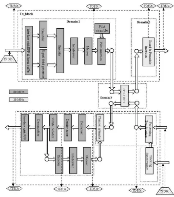
A block diagram of the Baseband processor is shown in Fig. 1. In order to achieve low power dissipation and to optimize silicon usage, the architecture is divided in two principle blocks: Transmitter and Receiver. According to this division, the baseband processing can provide two almost independent dataflow directions: transmit and receive.
The transmitter block consists of an input buffer, scrambler, signal field gener-ator, encoder, interleaver, mapper, 64-point IFFT/FFT (Inverse Fast Fourier Trans-form / Fast Fourier TransTrans-form) and circuitry for pilot insertion (with pilot scram-bler), guard interval insertion, and preamble insertion. The IFFT/FFT is a single block used in both, receive and transmit direction in order to optimize the baseband processor structure. On the other hand, this solution is more complex for imple-mentation, because of incomplete decoupling between the transmitter and receiver datapath.
ful-Fig. 1. Block diagram of the Baseband processor with embedded BIST.
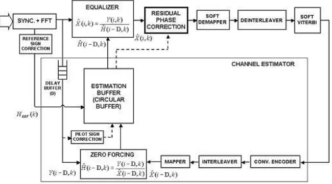
[image:3.612.103.460.74.478.2]Fig. 2. Block diagram of the proposed Channel Estimator.
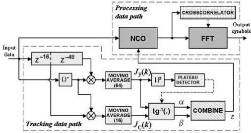
our design, a wide range of frequency offsets can be estimated ( 80 ppm) using only two autocorrelators. The output of one of those is also used in the frame de-tection mechanism. This provides a significant core area reduction in comparison with other proposed solutions, as in [4]. Here, the range of estimated frequency offsets is 40 ppm and three autocorrelators are used for the frame detection, but only two of them for the frequency offset estimation. In our design, frame detection is performed by a plateau detector, which has to detect a specific plateau shape in the incoming preamble symbols. The activity of the processing datapath starts after the frame is detected and the estimated value for frequency offset is available.
This part of the synchronizer performs the carrier frequency error correction, estimates the symbol timing and obtains the reference channel estimation. It con-sists of an NCO (Numerically Controlled Oscillator, in this case a CORDIC proces-sor operating in rotational mode), FFT procesproces-sor and a simplified crosscorrelator based on XNOR gates [3].
Channel estimation is based on a decision-directed method [5] with simplified residual phase estimation and correction mechanism. This type of channel esti-mation is based on a feedback loop. Therefore our receiver involves additional encoding, interleaving and mapping (Fig. 2). The interesting point in this concept is that it makes use of a division unit to correct the data samples (equalizer). The estimator is designed in such a way that the samples of symbol i are used to calcu-late an estimation of the channel, which will be used to correct the symboli D, whereDis the delay introduced by the feedback loop.
demap-Fig. 3. General scheme of the Synchronizer.
per, deinterleaver, descrambler, Viterbi decoder, and additional buffers.
In order to simplify processing of the data and optimize power consumption to the maximal extent, the complete structure was divided into two clock domains. Computationally complex blocks without high data throughput requirements were designed for 20 MHz and high data throughput demanding circuits were designed for 80 MHz.
3 Power Saving Issues in the Baseband Processor
[image:5.612.153.406.79.213.2]antee reliable operation it is necessary to provide a certain level of testability. A standard procedure in the synchronous world is to apply scan- based testing. In the case of the baseband processor we have decided not to use that approach. Scan test-ing could decrease performances of our system, and requires expensive hardware testers. Additionally, for datapath architectures Built-in Self-Test (BIST) could be designed in such way, that it tests most of the system functionality with very low cost in additional hardware and decreased performance.
It would be ideal if we could just in one run, perform testing of the complete baseband processor. Unfortunately, this baseband processor implementation does not allow that. The critical part is FFT/IFFT, which is a single block and can be either in transmit or receive mode and not both in the same time. All other parts in receiving and transmitting datapath are completely decoupled.
5 Implementation
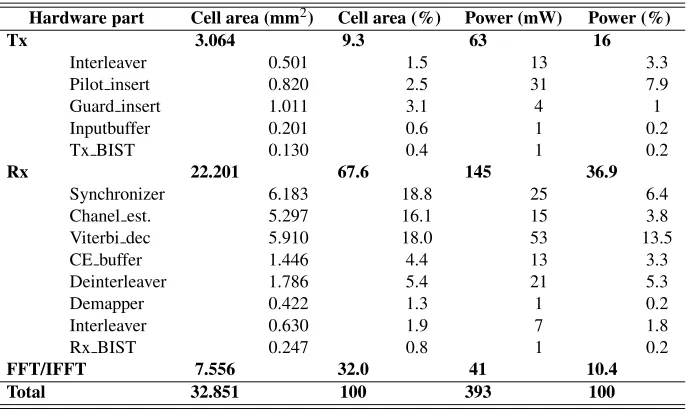
The complete baseband processor was modeled in VHDL and synthesized using our in-house 0.25 µm standard cell library. It‘s drawing cell area, including all blocks from Fig. 1, is 32,85 mm2 (equivalent transistor count is around 1
[image:7.612.111.457.370.575.2]Mil-lion). In Table 1 some synthesis results for our technology are given, whereT x indicates transmitter components andRx stands for receiver components. From Table 1 it can be noticed that the dominant hardware part is the receiver. It uses 67.6% of the chip cell area. Generally, the most silicon consuming components are synchronizer, channel estimator, Viterbi decoder and FFT/IFFT. Based on the result of the synthesis, the layout of the baseband chip is performed. According to after-layout power estimation with Synopsys Prime Power [6], the expected power consumption is 393 mW for the scenario of a real transceiver application. This application consists of the reception of 43 bytes and subsequent transmission of the standard acknowledge of 14 bytes. From this point of view most of the power is spent in the Viterbi processor (13.5%), FFT/IFFT (10.4%) and Transmitter in general (13%). One could observe that the total power spent in receiver is around 63.3 %. Remaining power is utilized by the clock tree, which impact is analyzed separately.
Table 1. Baseband processor synthesis results
Hardware part Cell area (mm2) Cell area (%) Power (mW) Power (%)
Tx 3.064 9.3 63 16
Interleaver 0.501 1.5 13 3.3
Pilot insert 0.820 2.5 31 7.9
Guard insert 1.011 3.1 4 1
Inputbuffer 0.201 0.6 1 0.2
Tx BIST 0.130 0.4 1 0.2
Rx 22.201 67.6 145 36.9
Synchronizer 6.183 18.8 25 6.4
Chanel est. 5.297 16.1 15 3.8
Viterbi dec 5.910 18.0 53 13.5
CE buffer 1.446 4.4 13 3.3
Deinterleaver 1.786 5.4 21 5.3
Demapper 0.422 1.3 1 0.2
Interleaver 0.630 1.9 7 1.8
Rx BIST 0.247 0.8 1 0.2
FFT/IFFT 7.556 32.0 41 10.4
Total 32.851 100 393 100
Fig. 4. Die photo of the Baseband chip.
6 Conclusions
This paper summarizes some research results from our Wireless Broadband Net-works project over the last five years. The implementation of the Baseband pro-cessor compliant with the IEEE 802.11a standard was a major task. In order to fulfill it, several innovative techniques were applied. In this paper the final struc-ture of the designed Baseband processor chip is described. The general scheme is explained and synthesis and layout results are presented. The circuitry, described here, is fabricated in IHP in-house 0.25µm CMOS technology.
References
[1] “IEEE p802.11a/d7.0, part 11: Wireless lan medium access control (mac) and physical layer (phy) specifications: High speed physical layer in the 5 GHz band,” Piscataway, NJ, 1999.
[2] E. Grasset al., “On the single-chip implementation of a hiperlan/2 and ieee 802.11a capable modem,”IEEE Personal Communications, vol. 8, no. 6, pp. 48–57, Dec. 2001. [3] M. Krstic, A. Troya, K. Maharatna, and E. Grass, “Optimized low-power synchronizer design for the IEEE 802.11a standard,” inProc. Int. Conf. on Acoustics, Speech and Signal Processing (ICASSP), vol. II, Apr.6–10, 2003, pp. 333–336.
[4] L. Schwoerer and H. Wirz, “Vlsi implementation of IEEE 802.11a physical layer,” in
[5] V. Mignone and A. Morello, “CD3-OFDM: A novel demodulation scheme for fixed and mobile receivers,”IEEE Trans. on Communications, vol. 44, no. 9, pp. 1144–1151, Sept. 1996.