UNIVERSITI TEKNIKAL MALAYSIA MELAKA
DETECTION OF DIELECTRIC MATERIAL USING
MINIATURE TWO-PLATE ELECTRICAL CAPACITANCE
SENSOR
This report is submitted in accordance with the requirement of Universiti Teknikal
Malaysia Melaka (UTeM) for the Bachelor of Electrical Engineering Technology (Industrial Electronics) with Honours
by
MOHD ALIF BIN MOHD TAH B071310205
91040301 - 01 - 6641
UNIVERSITI TEKNIKAL MALAYSIA
MELAKA
BORANG PENGESAHAN STATUS LAPORAN PROJEK SARJANA MUDA
TAJUK: DETECTION OF DIELECTRIC MATERIAL USING MINIATURE TWO-PLATE ELECTRICAL CAPACITANCE
SESI PENGAJIAN: 2016/17 Semester 1
Saya MOHD ALIF BIN MOHD TAH
mengaku membenarkan Laporan PSM ini disimpan di Perpustakaan Universiti Teknikal Malaysia Melaka (UTeM) dengan syarat-syarat kegunaan seperti berikut:
1. Laporan PSM adalah hak milik Universiti Teknikal Malaysia Melaka dan penulis. 2. Perpustakaan Universiti Teknikal Malaysia Melaka dibenarkan membuat salinan
untuk tujuan pengajian sahaja dengan izin penulis.
3. Perpustakaan dibenarkan membuat salinan laporan PSM ini sebagai bahan pertukaran antara institusi pengajian tinggi.
4. **Sila tandakan ( )
SULIT
TERHAD
TIDAK TERHAD
(Mengandungi maklumat yang berdarjah keselamatan atau kepentingan Malaysia sebagaimana yang termaktub dalam AKTA RAHSIA RASMI 1972)
(Mengandungi maklumat TERHAD yang telah ditentukan oleh organisasi/badan di mana penyelidikan dijalankan)
Alif
Alamat Tetap:
No 26, JLN LUMPIT 24,
TAMAN TERATAI KANGKARPULAI,
81110 JOHOR BAHRU
Disahkan oleh:
DECLARATION
I hereby, declared this report entitled “PSM Title” is the results of my own research except as cited in references.
Signature :
Alif
Author’s Name : MOHD ALIF BIN MOHD TAH
APPROVAL
This report is submitted to the Faculty of Engineering Technology of UTeM as a partial fulfillment of the requirements for the degree of Bachelor of Electrical Engineering Technology (Industrial Electronic) with Honours. The member of the supervisory is as follow:
Wan Norhisyam
ABSTRAK
Penderia kemuatan elektrik untuk mengesan bahan dielektrik dibina dan dibentangkan dalam kerja ini. Projek ini memberi tumpuan kepada bagaimana untuk mereka bentuk dan melaksanakan sistem untuk mengesan jenis bahan dielektrik menggunakan ujian kemuatan elektrik. Penderia kemuatan Elektrik direka dengan menggunakan perisian Comsol Multiphysics untuk melihat medan elektrik dan kontur potensi elektrik. Nilai kemuatan dari perisian diukur berdasarkan konsep litar ulang alik. Arus dari penderia mengalir ke litar pengesan cas dimana nilai voltan ialah berpadanan dengan nilai kemuatan antara sepasang elektrod. Voltan dari litar pengesan cas telah dikuatkan oleh litar penguat sebelum menghantar kepada litar penapis untuk menolak isyarat yang tidak diingini dan untuk mendapatkan keluaran arus terus yang bersih dari isyarat masukan ulang alik. Voltan daripada litar penapis
ABSTRACT
DEDICATION
Special dedicated to
ACKNOWLEDGEMENT
A lot thanks to Allah the Almighty give me this opportunity to finish my final Degree project. Indeed, the lessons learnt gained my knowledge and opened me up to new perspectives. In the name of Allah, most benevolent, ever-merciful, all praises be to Allah, Lords of all the worlds. Thank you Allah.
First of all, I would like to extend my supreme appreciation to my supervisor Wan Norhisyam Bin Abd Rashid for his enthusiasm, support and endless advice towards my project. His help and constant encouragement have given me valuable inputs from time to time throughout my study. He puts a tremendous amount of effort into providing opportunities for me to learn and to grow. I would also like to give my sincerely a lot thanks to Ir Mohammad’ Afif Bin Kasno and Ir Nik Azran Bin Abdul Hadi who have spent her valuable time reviewing few of my project and giving his valuable suggestions.
My deepest gratitude, million thanks and appreciation also goes to my beloved father and mother for their blessings, patience and unconditional love. Thanks also to my siblings, who has given me his absolute and constant encouragement and infinitive support from beginning to the end of this project. Last but not least, many thanks also to all lecturers and members either directly or indirectly who are contribute help and support in solving this project. Thank you
TABLE OF CONTENT
Abstrak i
Abstract ii
Dedication iii
Acknowledgement iv
Table of Content v
List of Tables viii
List of Figures ix
List Abbreviations, Symbols and Nomenclatures xii
CHAPTER 1: INTRODUCTION
1.0 Background of project 1
1.1 Problem Statement 3
1.2 Objective of project 3
1.3 Scope of Study 4
1.4 Thesis Outline 4
CHAPTER 2: LITERATURE REVIEW
2.0 Introduction 6
2.1 Non-destructive Testing Method 6
2.1.1 Radiography (RT) 7
2.1.1.1 Fundamental Principle 7
2.1.1.2 How it work 7
2.1.1.3 Advantages and disadvantages 9
2.1.2 Ultrasound (UT) 9
2.1.2.1 Fundamental Principle 9
2.1.2.2 How it work 10
2.1.2.3 Advantages and disadvantages 11
2.1.3 Liquid Penetrant (PT) 12
2.1.3.1 Fundamental Principle 12
2.1.3.3 Advantages and disadvantages 13 2.1.4 Magnetic particle Inspection (MPI) 14
2.1.4.1 Fundamental Principle 14
2.1.4.2 How it work 15
2.1.4.3 Advantages and disadvantages 16
2.1.5 Eddy Current Testing (ECT) 16
2.1.5.1 Fundamental Principle 16
2.1.5.2 How it work 17
2.1.5.3 Advantages and disadvantages 18 2.2 Non-Destructive Testing Methods & Applications Flaw 19 2.3 Electrical Capacitance Sensor Design 21 2.4 Factors in designing Electrical Capacitance Sensor 21
CHAPTER 3: METHODOLGY
3.0 Introduction 22
3.1 Flow of the project 22
3.1.1 Description of flowchart 24
3.2 Overview of the system 25
3.2.1 Description of block diagram 26
3.3 Electrical Capacitance design in Comsol Multiphysic Software 26 3.3.1 Decide on the representative physics 26 3.3.1.1 Select 2D as Space Dimension 26 3.3.1.2 Select Electrostatics as type of physics 27 3.3.1.3 Select Stationary as type of study 28 3.3.1.4 Define the geometry on which to solve the problem 29 3.3.1.5 Set the material properties 29
3.4 Sensor model 30
3.4.1 Electrical Capacitance Sensor design prototype 31
3.5 Graphical User Interface 32
CHAPTER 4: RESULTS AND DISCUSSION
4.1 Comsol Simulation 34
4.1.1 Relationship between Capacitance Value to the length of
electrodes 34
4.1.2 Relationship between Capacitance Value to the length of
electrodes 45
4.2 Hardware Results 56
4.2.1 Standing Capacitance 56
4.2.2 Position of the material 57
4.2.3 Distance between two electrodes 59
4.2.4 Angle between two electrodes 61
4.2.5 labVIEW interface 64
CHAPTER 5: CONCLUSION AND FUTURE WORK
5.1 Conclusion 67
5.2 Significant Contributions towards Process Electrical
Capacitance Sensor 68
5.3 Recommendations for Future Work 68
REFERENCES 69
APPENDICES
A Gantt chart
viii
LIST OF TABLES
2.1 Non-Destructive Testing Methods & Application Flaws 19
4.1 4.2 4.3 4.4 4.5
4.6
The relationship between capacitance and length of electrodes The relationship between capacitance and number of electrodes The relationship between capacitance and frequency
The relationship between capacitance and position
The relationship between voltage and distance between two plates
The relationship between voltage and angle between two plates
43 54 56 58 59
LIST OF FIGURES
1.1 Overview of an ECS system 2
1.2 Connection of driven guard 2
2.1 Illustration of Radiography Testing 8
2.2 Illustration of Ultrasonic flaw detection 11 2.3
2.4 2.5
Illustration of Dye penetrating Testing
Illustration of the principle of Magnetic Particle Inspection Test An Illustration of the Eddy Current Equipment
13 16 18
3.1 Flow Chart of the system 24
3.2 Block diagram of the system 25
3.3 Space Dimension 26
3.4 3.5 3.6 3.7 3.8 3.9 4.1 4.2 4.3 4.4 Physics interface Study Interface
Graphical User Interface for Comsol 2D models for parallel two-plates of ECS labVIEW interface
Experiment set-up
The electrical potential and electric field for single excited electrodes when length of electrodes = 20mm and distance between two electrodes = 30mm.
The electrical potential and electric field for single excited electrodes when length of electrodes = 20mm and distance between two electrodes = 40mm.
The electrical potential and electric field for single excited electrodes when length of electrodes = 20mm and distance between two electrodes = 50mm.
The electrical potential and electric field for single excited
electrodes when length of electrodes = 40mm and distance between two electrodes = 30mm.
4.5 The electrical potential and electric field for single excited electrodes when length of electrodes = 40mm and distance between two electrodes = 40mm.
38
4.6 The electrical potential and electric field for single excited electrodes when length of electrodes = 40mm and distance between two electrodes = 50mm.
39
4.7
4.8
4.9
The electrical potential and electric field for single excited electrodes when length of electrodes = 60mm and distance between two electrodes = 30mm.
The electrical potential and electric field for single excited electrodes when length of electrodes = 60mm and distance between two electrodes = 40mm.
The electrical potential and electric field for single excited electrodes when length of electrodes = 60mm and distance between two electrodes = 50mm.
40
41
42
4.10 The electrical potential and electric field for single excited electrodes when distance between two electrodes = 30mm for 4electrodes 45 4.11 4.12 4.13 4.14
The electrical potential and electric field for single excited electrodes when distance between two electrodes = 40mm for 4electrodes
The electrical potential and electric field for single excited electrodes when distance between two electrodes = 50mm for 4electrodes
The electrical potential and electric field for single excited electrodes when distance between two electrodes = 30mm for 6electrodes
The electrical potential and electric field for single excited
46
47
48
xi electrodes when distance between two electrodes = 50mm for
6electrodes
4.16 The electrical potential and electric field for single excited electrodes when distance between two electrodes = 30mm for 8electrodes
51
4.17 The electrical potential and electric field for single excited electrodes when distance between two electrodes = 40mm for 8electrodes
52
4.18 The electrical potential and electric field for single excited electrodes when distance between two electrodes = 50mm for 8electrodes 53 4.19 4.20 4.21 4.22 4.23 4.24 4.25 4.26 4.27
Standing capacitance of the material The position of the material
Capacitance Value toward it position
Output Voltage of the material and distance between two plates The angle of ECS
The Relationship Output Voltage of the material and angle between two plates
labVIEW results when ECS detects material of paper labVIEW results when ECS detects material of FR4 labVIEW results when ECS detects material of strip board
LIST OF ABBREVIATIONS, SYMBOLS AND
NOMENCLATURE
AC - Alternating Current
ADC - Analog to digital converter DAS - Data acquisition system
ECT - Electrical Capacitance Tomography ECS - Electrical Capacitance Sensor GUI - Graphical User Interface mm - millimetres
Op-amp - Operational amplifier PC - Personal Computer PCB - Printed Circuit Board USB - Universal Serial Bus Vp-p - Voltage peak-to-peak A/D - Analog to Digital
f - Frequency
Cx - Unknown standing capacitance d - Distance between of two plates ε0 - Permittivity of free space εr - Relative Permittivity
CHAPTER 1
INTRODUCTION
1.0 Background of project
Electrical Capacitance Sensor (ECS) is a type of a non- destructive testing technique. This system is adopted from the Electrical Capacitance Tomography (ECT) concept which is become utmost mature between various tomography modalities. The concept operation of the system is to measure the variations of capacitance between two plates of electrodes representative the permittivity distribution and hence the material distribution (Yang & Peng, 2013). Any two adjacent conductors can be considering as a capacitor and different dielectric properties between conductors will create a different capacitance value (Mohamad et al. 2011).
. Each of the dielectric material has different permittivity value so it will result the different capacitance value. This system consists of three main parts which are electrode capacitance sensor, a capacitance measuring unit and a host of computer as shown in figure 1.1. The capacitance measuring circuit or known as signal conditioning circuit is used to collect data and convert the measuring reading to digital (Mohamad, 2012) before the computer manipulate and display the results.
manufacturing application including movement measurement in oil pipelines (Li, 2013),(Xie et al. 1992), wet gas separators, fluidized beds(Liu, Chen & Wang, 2005 ),(Liu, Yang & Wang, 2011),(Warsito & Fan, 2005),(Warsito & Fan, 2003), pneumatic conveyors and gas/solids cyclones(Wang, Liu, Jiang & Yang, 2006). The purpose of the research is to investigate the output voltage corresponding to the capacitance value of the Electrical capacitance Sensor on dielectric materials test on paper, plastic and FR4 board.
[image:18.595.199.424.473.624.2].
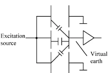
Figure 1.1 Overview of an ECS system
Figure 1.2 Connection of driven guard electrodes Sensor
Display type of the material
1.2 Problem Statement
The ECS design has been linked to many issues. From that, here are several subjects which were highlighted and discussed as follows:
i. The measurement of internal electrode capacitance with the permittivity distribution and potential distribution is difficult using Laplace Equation. Therefore, by using Finite element method (FEM) simulation package is so much useful.
ii. The sensitivity in dissimilar location between the electrode pair can differ radically where the sensitivity distribution is not uniform. This is because of the evident attribute of soft-field sensing.
iii. To reduce the noise, driven guard electrodes is introduced to eliminate the fringe effect when measure internal electrode capacitance.
1.3 Objectives
At the completion of tasks project, I will able:
i. To design the Electrical Capacitance Sensor (ECS) using Comsol Multiphysics Software
ii. To study the performance of Electrical Capacitance Sensor iii. To develop an Electrical Capacitance Sensor to detect the type of
1.4 Scope of Study
The focus of the project will be on:
i. Design an Electrical Capacitance Sensor in 2D using AC/DC (electrostatics) module in Comsol Multiphysics Software.
ii. The number of 2,4,6,8 electrodes, distance between two plates and the length of electrodes are considered in design of Electrical Capacitance Sensor in Comsol Software to see it performance when detect the dielectric materials.
iii. Development of two electrodes of ECS to test material distribution of FR4, paper and Strip board.
1.5 Thesis outline
The thesis report is divided into six chapters where each of the chapter is briefly described as follow:
First chapter is describing the background of study, problem statement, objectives of the project and research scopes.
Second chapter presents the literature review of the project. It discussed about the introduction about dielectric material, non- invasive testing method that available used in industry to detect the dielectric material and some previous research paper related to my project.
is measured and development labVIEW software as graphical human interface (GUI).
The fourth chapter describes analysis and explanation about the results and discussions for software and hardware of this project.
The fifth chapter is describing the conclusions of finding results and suggestions for future work.
CHAPTER 2
LITERATURE REVIEW
2.0 Introduction
A composite material is a structural material that has two or more combined constituents that are joint at a macroscopic level and are not soluble in each other. Besides that, advanced composite materials that are traditionally available used in the aerospace and another industries commercial as well (Kaw & Group 2006). It is fact that there are inherent flaw in composite material. Manufacturing process like welding, casting, forging, surface treatment and many more industrial applications may cause further flaws or defects.
Therefore, there are several of non - destructive methods (NDT) that can be used to evaluate the materials and at the same time can appraise in term of size, nature and place (International Atomic Energy Agency, 2001). Each of NDT method has advantages and disadvantages for a given application. From that, to select NDT method properly is very important that will give the necessary results.
2.1 Non-destructive Testing Method
,PT, Magnetic Particle Inspection, MPI) and Eddy Current Testing, ECT(Kufrin et al.
2010),( Garcia-Martin et al. 2011), (Stubendekova et al. 2014).
2.1.1 Radiography (RT)
2.1.1.1 Fundamental Principle
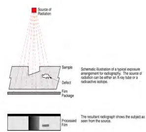
Radiography is a non-destructive inspection way that used short wavelength electromagnetic radiation passing through the material. This method is useful for the detection of internal defect or flaws in ferrous or lower material density allow more and so that absorb less. In addition, the radiation which reaches the film after passing through the materials becomes a shadow image in a
photographic film. The area of low absorption looks dark areas on the developed film, while the area of high absorption looks as light area on the developed film.
2.1.1.2 How it works
The act of an electron striking the target produces X-rays which these are produced only voltage is applied to the X-ray tube. Whether using X-rays or gamma sources, the test object for example weld is not radioactive following the inspection. Subsurface discontinuities that are readily discovered by this method are voids instead rounded flaws, metallic and non-metallic inclusion and also favorably aligned incomplete fusion and flaws. Void such as porosity form dark area on the film because they represent a significant loss of a material. Furthermore, metallic inclusions form light area if they are denser than the test object
Figure 2.1 Illustration of Radiography Testing
2.1.1.3 Advantages and disadvantages