Abstract: This paper presents the prototype and simulations of a compact rectangular microstrip patch antenna for ultra-wideband applications. The proposed antenna is printed on FR4 (Flame Retardant) substrate with relative permittivity of 4.4, dielectric loss tangent of 0.0024 and the dimensions of 57 × 25 × 1.57 mm3. The radiating patch of the antenna is loaded with two rectangular stubs along its upper and lower edges and an equilateral triangular notch is truncated from the reduced ground plane to achieve optimum results in terms of bandwidth and reflection coefficient. It is fed along the centerline of symmetry by 50Ω microstrip feed line. The simulated return loss ( ) characteristics show that the proposed antenna has a capability of covering the wireless bands from 0.17GHz to 7.25GHz with impedance bandwidth of 7.08GHz and exhibits a peak gain of 5dB at 7.25GHz which is acceptable for UWB systems.
Index Terms: UWB patch antenna, DGS (Defected ground structure), VSWR (Voltage Standing Wave Ratio), Smith Chart, Radiation Pattern, CST MWS’14.
I. INTRODUCTION
In the recent years, the development of UWB technology has played a very crucial role in wireless communication systems to meet the ever-increasing demands of large bandwidth and high data transmission rate with low power consumption and little interference for short distance wireless communications amongst the users [1]. The UWB signal employs the bandwidth greater than 20% of the center frequency or at least 500MHz. The UWB radio system covers the frequency band from 3.1GHz to 10.6GHz which is based on the concept of transmitting and receiving data by employing narrow pulses of very short duration (order of few nanoseconds or less) at extremely low power that spread out over wide bandwidth [2]. UWB antennas have gained considerable acceptance in various fields of wireless communications such as GPS, fast peer-to-peer communication for short distances (10m), satellite and missile applications, weather forecast, medical sensing, radar and sensing applications, home electronics and many more [3].
This equipment working on UWB require small sized antennas for the apparatus to be handy. Microstrip patch antenna supports all the properties of being small and compact in size and hence can be utilized in this equipment. Covering an UWB with these microstrip patch antenna is a challenge as they suffer from the problem of low bandwidth of 5% due to excitation losses of surface wave radiation [4].
Revised Manuscript Received on July 12, 2019.
Arashpreet Kaur, ECED, Thapar Institute of Technology, Patiala,
India.
Amanpreet Kaur, ECED, Thapar Institute of Technology, Patiala, India.
Many techniques have been introduced in past few years to overcome this problem such as increase substrate thickness [5], staircase geometry [6], slotted antenna geometry [7], probe-feeding technique [8], DGS technique [9], stacked patch antenna [10], tuning stub [11] etc.
Generally, conventional slotted patch antennas can be used to achieve multiband and dual band behaviour but fails to cover an ultra-wideband range. The size and shape of the radiator are major elements that must be considered while designing an UWB antenna. In order to achieve an UWB range, the slots and notches should be engraved from the radiating patch in such a manner that maximum current distribution remains along the edges of the radiator [12]. One of most appropriate method to achieve an ultra-wideband and miniaturization characteristic is by employing different defective ground structure geometries such as dumbbell shape DGS [13], U-shaped DGS [14], circular dumbbell shape DGS [15], Cross shaped DGS [16] etc.
In this paper, a compact UWB patch antenna loaded with stubs and a reduced ground plane with DGS is proposed for early detection of breast cancer using mono-static radar based active microwave imaging technique. It covers the wireless bands from 0.17GHz to 7.25GHz with impedance bandwidth of 7.08GHz which is acceptable for UWB operation (3.1-7.25GHz), GSM (Global System for Mobile Communications) (800-900MHz, 1800-1900MHz), WLAN (Wireless Local Area Networks) applications (2.4-2.485GHz,
5.15-5.535GHz, 5.725-5.825GHz), Bluetooth
(2.4-2.483GHz), Microwave ovens (2450MHz), Zig-Bee (2.4-2.485GHz), WiMAX (Worldwide Interoperability for Microwave Access) (3.4-3.69GHz), IMT (International Mobile Telecommunications) band (3.4-3.6GHz), INSAT (Indian National Satellite System) (4.5-4.8 GHz), Radio Astronomy Band (5.01-5.03GHz) and STM (Synchronous Transport Module) band applications (6-6.17GHz). All the designing and simulations are implemented in CST MWS’14.
II. ANTENNADESIGNANDSPECIFICATIONS In order to design an UWB microwave antenna, compact rectangular antenna geometry loaded with stubs and a reduced ground plane with DGS is proposed. Fig. 1(a) shows the top view of the proposed antenna which consists of a rectangular radiating patch joined with two rectangular stubs, one along its lower edge with length (d) and width (c) of 5mm and 8mm respectively and other along its upper edge with length (a) and width (b) of 5mm and 6mm respectively, to achieve an optimum UWB operation.
The proposed antenna is fabricated on FR4 substrate with relative permittivity ( )
A Compact Rectangular Microstrip Patch
Antenna Loaded with Stubs and Defected Partial
Ground Structure for UWB Systems
of 4.4, dielectric loss tangent value of 0.0024 and dimensions of 57 × 25 × 1.57 mm3. The dimensions of the rectangular radiating patch are optimized and the desired results are obtained for length (Lp) and width (Wp) of 25mm and 17.8mm respectively. The patch antenna is excited along its centerline of symmetry through microstrip feed line with characteristic impedance of 50 . Initially, the length of the feed line is varied and best antenna performance in terms of impedance bandwidth is obtained for length and width (f) of 1mm and 3.4mm respectively.
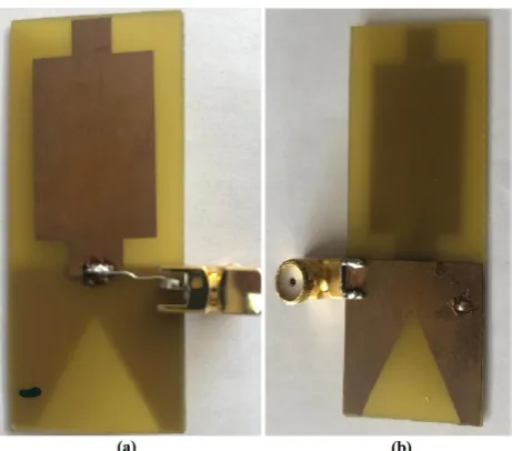
Fig. 1. Proposed antenna (a) Top view with rectangular radiating patch loaded with stubs (b) Bottom view with
[image:2.595.303.550.215.450.2]reduced DGS
Fig. 2. Snapshot of the fabricated antenna (a) Top view with rectangular radiating patch with the SMA connector (extended with a lossless cable) (b) Bottom view with reduced
DGS
Fig. 1(b) shows a reduced ground plane with length (Lg) and width (Wg) of 22mm and 25mm respectively with an equilateral triangular notch engraved along its lower edge for shifting the frequency band towards left and to improve return loss ( ) characteristics. For dominant mode , the side of equilateral triangular notch (s) is calculated using the following expression [17]:
(1)
where c, and are speed of light, resonant frequency and dielectric constant respectively. By evaluating c = 3x m/s, =5.1GHz and =4.4 in Eq. (1), the side of equilateral notch comes out to be 18mm. The dimensions of patch, dielectric substrate and the ground plane are calculated using transmission line model equations. Fig. 2(a) and 2(b) shows the top view and bottom view of the fabricated microstrip-fed antenna respectively soldered with a SMA (Sub Miniature Version A connector). The detailed dimensions of the various antenna parameters are summarized in Table 1.
Table 1. Optimized Design Parameters of the proposed antenna
Parameter Description Value
Lq Length of substrate 57mm
Wq Width of substrate 25mm
Lp Length of rectangular
patch
25mm
Wp Width of rectangular
patch
17.8mm
Lg Length of ground 22mm
Wg Width of ground 25mm
f Width of feed line 3.4mm
a Length of upper stub 5mm
b Width of upper stub 6mm
c Width of lower stub 8mm
d Length of lower stub 5mm
s Side of equilateral
triangular notch
18mm
III. SIMULATIONRESULTSANDDISCUSSIONS To analyze the capabilities of the proposed antenna, it is designed and simulated in CST MWS’ 14 software package which provides fast and accurate analysis of high frequency equipments. The antenna performance parameters such return loss and gain are investigated in this section.
A. Return Loss and Impedance Bandwidth
Fig. 3 shows the simulated (dB) parameter plot of the proposed antenna which varies as the function of frequency. The return loss is measured below -10dB and impedance bandwidth is the frequency range for which the antenna sustains the given return loss characteristics [18]. The proposed antenna covers an operational band from 0.17GHz to 7.25GHz with impedance bandwidth of 7.08GHz. This helps to make the antenna appropriate for UWB operation (3.1-7.25GHz), GSM mobile phones (800-900MHz, 1800-1900MHz), WLAN applications (2.4-2.485GHz, 5.15-5.535 GHz, 5.725-5.825GHz), Bluetooth (2.4-2.483
GHz), Microwave ovens (2450MHz), Zig-Bee
(2.4-2.485GHz), WiMAX (3.4-3.69GHz), IMT band (3.4-3.6GHz), INSAT (4.5-4.8 GHz), Radio Astronomy Band (5.01-5.03GHz) and STM
band applications
[image:2.595.53.284.385.588.2]shown at 1.5GHz resonant frequency which depicts that the proposed antenna provides good impedance matching performance with least power loss.
Fig. 3. Simulated Return Loss ( ) versus frequency plot of the proposed antenna
B. Gain
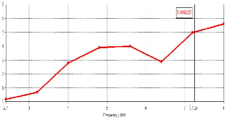
[image:3.595.52.288.98.216.2]Fig. 4 shows gain plot of the proposed antenna for the specified operational frequency range. High gain antennas are preferred for long distance applications [19]. It is observed that the gain is greater than 3dB for the frequency range from 4.15GHz to 6.3GHz and from 6.4GHz to 7.25GHz which acceptable for practical applications. A peak gain of 5dB is achieved at 7.25GHz frequency. Figure 5(a) show the 3D view peak gain of the proposed antenna at 7.25GHz frequency. Fig. 5(b) and 5(c) illustrates the polar gain characteristics plots of the proposed antenna at 7.25GHz frequency. The elevation plane pattern of proposed antenna has a major lobe directed at an angle of -94 degrees with half power beam width of 74.2degrees. The azimuth plane pattern of proposed antenna has a major lobe which is directed at an angle of 47 degrees with magnitude of 3.34dB and angular beam width of 47.5degrees.
Fig. 4. Simulated gain versus frequency plot of the proposed antenna
Fig. 5. Proposed antenna (a) 3D plot of peak gain at 7.25GHz frequency (b) Polar gain plot for Elevation plane at 7.25GHz frequency (c) Polar gain plot for Azimuth plane at 7.25GHz
frequency
C. Smith Chart
[image:3.595.319.535.400.540.2]The smith chart plot of the proposed UWB antenna is shown in Fig. 6. Smith chart is defined as the polar plot of complex reflection coefficient with respect to frequency. The locus of the smith chart should intersect its center for perfect impedance matching of antenna [20]. The proposed antenna gives impedance of 50 ohms which is acceptable for practical applications. The markers 1 and 2 in Fig.6 represent the bandwidth of 7.08 GHz in frequency range of 0.17GHz to 7.25GHz. Hence the antenna is perfectly matched.
Fig. 6. Smith Chart of proposed antenna
D. VSWR (Voltage Standing Wave Ratio)
[image:3.595.53.285.488.610.2]Fig. 7. VSWR of proposed antenna
E. Surface Current
[image:4.595.51.301.57.169.2]As shown in Fig. 8(a-f), the proposed antenna is energized with 1W power at the feed point to observe the surface current distribution on the rectangular radiating patch and the reduced ground with DGS at 1.5GHz, 5.07GHz and 6.9GHz resonant frequencies. Fig. 8(a) show that more magnitude of current is distributed along the lower boundaries of the lower stub of the rectangular patch joined to the feed line at 1.5GHz frequency. Fig. 8(b) shows that highest magnitude of the current (157A/m) is present in the region just behind the feed line in the reduced ground which excites resonance at 1.5GHz frequency. Fig. 8(c) show that maximum current (69.6A/m) is flowing along the lower boundaries of the lower stub of the rectangular patch attached to the feed line which excites resonant frequency of 5.07GHz. Fig. 8(d) the show that more magnitude of current is in the region just behind the feed line in the ground at 5.07GHz frequency. Fig. 8(e) shows that the highest current (59.6 A/m) is flowing along the boundaries of the lower stub which is attached to the feed line which excites resonant frequency of 6.9GHz. Fig. 8(f) shows that more current is flowing in the region just behind the feed line in the reduced ground plane at a resonant frequency of 6.9GHz.
Fig. 8. Surface current distributions on the radiating patch and reduced ground plane at resonant frequencies of (a-b) 1.5GHz
(c-d) 5.07GHz (e-f) 6.9GHz
This is further illustrated by parametric variations carried out to optimize the proposed antenna in the next section.
IV. EFFECT OF PARAMETRIC VARIATIONS ON RETURN LOSS (
The major aim of the proposed antenna design is to achieve miniaturization and ultra-wideband characteristics. In this section, various design parameters such as ground plane, stubs and feedline influencing the antenna characteristics are investigated and optimized in order to improve antenna performance for return loss and to achieve UWB.
A. Effect of Reduced Ground with DGS
Fig. 9(a-b) illustrates the design procedure of a reduced ground plane with DGS and its parametric dimensions are summarized in Table 1. Fig. 10 shows the comparison plots of simulated return loss ( ) values versus frequency for different ground geometries while keeping other design parameters constant. The reduced ground with length 22mm as shown in Fig. 9(b) covers a large operational band from 0.47GHz to 7.27GHz with bandwidth of 6.8GHz as compared to ground plane with length of 57mm as shown in Fig. 9(a) which covers the frequency range from 14.03GHz to 14.38GHz. For improving the impedance matching performance of the proposed antenna, an equilateral triangular notch is etched
[image:4.595.47.272.476.659.2]loss from -23.52dB to -29.74dB and covers an ultra-wideband from 0.17GHz to 7.25GHz with bandwidth of 7.08GHz. It can be concluded that the proposed antenna with DGS offers wider bandwidth and good impedance matching performance as compared to without DGS.
Fig. 9. Proposed antenna design (a) Full ground plane with length 57mm (b) Reduced ground with length 22mm (c)
[image:5.595.48.278.117.212.2]Reduced ground with length 22mm and an equilateral triangular notch of side 18mm
Fig. 10. Comparisons of Simulated Return Loss ( ) curve against frequency for different ground geometries
B. Effect of Varying the Feed Length
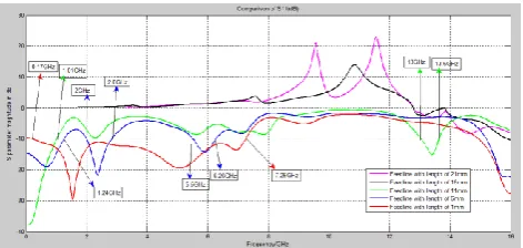
Fig. 11 shows the design procedure for different length of the feed line while keeping other design parameters constant. Fig. 12 shows the comparison plots of parameter versus frequency for different lengths of feed line which is varied from 21mm to 1mm. The return loss is measured at -10dB which shows that the feed lengths of 21mm and 16mm are not appropriate for the proposed antenna. The major aim of the proposed antenna is to achieve UWB characteristics. The feed line with lengths of 11mm and 6mm offers dual band and multiband behaviour respectively. The feed line with length of 1mm provides best optimized results and covers a wide frequency range from 0.17GHz to 7.25GHz with bandwidth of 7.08GHz and provides three resonant peaks of -29.74dB, -19.6dB and -14.04dB at frequencies of 1.5GHz, 5.07GHz and 6.9GHz respectively.
Fig. 11. Proposed antenna designs with feed length of (a) 21mm (b) 16mm (c) 11mm (d) 6mm (e) 1mm
Fig. 12. Comparisons of Simulated Return Loss ( ) curves against frequency by varying the feed length
C. Effect of Stubs to the Patch shape
[image:5.595.46.283.279.392.2]Fig. 13(a-c) illustrate the different geometries of radiating patch with addition of stubs and its parametric dimensions are listed in Table 1. Fig.14 show the comparison of the simulated return loss curves against frequency for different patch geometries. Fig. 13(a) shows a rectangular radiating patch which exhibits dual band behaviour. To achieve an UWB behaviour, a rectangular stub is added to the lower end of the radiating patch which offers the bandwidth of 6.08GHz. For improving the impedance matching performance and bandwidth of the proposed antenna, one more rectangular stub is joined to the radiating patch at its upper end as shown in Fig. 13 (c). It covers the wide frequency range from 0.17GHz to 7.25GHz with bandwidth of 7.08GHz which makes the antenna appropriate for large number of wireless applications.
Fig. 13. Proposed antenna design for (a) Simple rectangular patch (b) Rectangular patch joined with a stub (c) Rectangular
[image:5.595.305.544.409.529.2]patch joined with two stubs
Fig.14. Comparisons of Simulated Return Loss ( ) curves against frequency for different patch geometries
V. CONCLUSION
[image:5.595.309.546.583.709.2] [image:5.595.47.285.642.743.2]stubs and a reduced ground with DGS has been successfully prototyped and simulated in this article. The dimensions of the ground plane, stubs and feed line are optimized to achieve an optimum UWB operation. The simulated results show that the proposed antenna efficiently radiates from 0.17GHz to 7.25GHz with the fractional bandwidth of 0.8 and peak gain of 5dB at 7.25GHz frequency. It covers the wireless applications such as GSM mobile phones (800-900MHz, 1800-1900MHz), WLAN applications (2.4-2.485GHz, 5.15-5.535GHz, 5.725-5.825GHz), Bluetooth (2.4-2.483
GHz), Microwave oven (2450MHz), Zig-Bee
(2.4-2.485GHz), WiMAX (3.4-3.69GHz), IMT band (3.4-3.6GHz), INSAT (4.5-4.8GHz), Radio Astronomy Band (5.01-5.03GHz), STM band applications (6-6.17GHz). In future, the measured results can be obtained to verify the proposed antenna design for practical applications.
ACKNOWLEDGEMENTS
We would like evince a deep sense of gratitude to the entire staff and faculty of Electronics and Communication Engineering Department of Thapar University, Patiala for providing adequate facilities and environment for the successful completion of this research work.
REFERENCES
[1]Vuong, T.P., Ghiotto, A., Tedjini, S., et al. (2007). Design and characteristics of a small U-slotted planar antenna for IR-UWB.
Microwave and Optical Technology Letters, 49(7), 1727-1731. [2]Jung, J., Choi, W., Choi, J., (2005). A Small Wideband Microstrip-fed
Monopole Antenna. IEEE Microwave and Wireless Components Letters, 15(10), 703-705.
[3]Kaur, S., Khanna, R., (2015). Design and analysis of stair-shape antenna with flowery DGS. International Journal of Microwave and Wireless Technologies, 7(1), 53-60.
[4]Balanis, C.A. (2005). Antenna Theory Analysis and Design, 3rd edition.
Hoboken, NJ: John Wiley & Sons, Inc.
[5]Abdelaziz, A.A. (2006). Bandwidth enhancement of microstrip antenna.
Progress in Electromagnetics Research, PIER 63, 311–317. [6]Kaur, A., Kaur, A. (2017). A compact staircase shaped slotted microstrip
patch antenna with DGS for UWB applications. 5th International Conference on Advancements in Engineering and Technology, Sangrur, India, 66-69.
[7]Lee, C.P., Chakrabarty, C.K. (2011) Ultra-Wideband Microstrip Diamond Slotted Patch Antenna with Enhanced Bandwidth.
International Journal of Communications, Network and System Sciences, 4(7), 468-474.
[8]Islam, M.T. (2009). Design analysis of High Gain Wideband L-Probe fed Microstrip Patch Antenna. Progress in Electromagnetics Research, PIER 95, 397-407.
[9]Kaur, A., Khanna, R., Kartikeyan, M.V. (2015). A stacked Sierpinski gasket fractal antenna with defected ground structure for UWB/WLAN/radio astronomy/STM link applications. Microwave and Optical Technology Letters, 57(12), 2786-2792.
[10] Kaur, A., Khanna, R. (2017). Design and development of a stacked complementary microstrip antenna with a ‘ ’-shaped DGS for UWB, UNII, WLAN, WiMAX and radio astronomy wireless applications.
International Journal of Microwave and Wireless Technologies, 2, 1-10.
[11] Kaur, A., Kaur, A. (2017). An extended semi-circular microstrip patch antenna with DGS for UWB applications. Journal of Microwave Engineering and Technology, 4(1), 13-18.
[12] Wu, C.M., Chen, Y.L., Wen, C.L. (2012). A Compact Ultra-Wideband Slotted Patch Antenna for Wireless Dongle Application. IEEE Antennas and Wireless Propagation Letters, 11, 596-599.
[13] Arya, A.K., Patnaik, A., Kartikeyan, M.V. (2013). Gain Enhancement of Microstrip patch antenna using Dumbbell shaped Defected Ground Structure. International Journal of Scientific Research Engineering and Technology, 2(4), 184-188.
[14] Woo D.J., Lee, T.K., Lee, J.W, Pyo, C.S, Choi, W.K. (2006). Novel U-Slot and V-Slot DGSs for band stop filter with improved Q-factor. IEEE Transactions on Microwave Theory Techniques, 54(6), 2840-2847.
[15] Reddy, B.R., Vakula, D. (2015). Compact Zigzag Shaped Slit Microstrip Antenna with Circular Defected Ground Structure for Wireless Applications, IEEE Antennas and Wireless Propagation Letters, 14, 678-681.
[16] Chen, H.J., Huang, T.H., Chang, C.S., Chen, I.S., Wang, N.F., Wang, Y.H, Houng, M.P. (2007). A novel cross-shape DGS applied to the design of ultra-wide stop band low pass filters. IEEE Microwave Wireless Components Letters, 17(8), 586-588.
[17] Chen, W., Lee, K.F., Dahele, J.S. (1992). Theoretical and experimental studies of resonant frequencies of the equilateral triangular microstrip antenna. IEEE Transactions on Antennas and Propagation, 40(10), 1253-1256.
[18] Kaur, A., Khanna, R., Kartikeyan, M.V. (2017). A Multilayer dual wideband circularly polarized Microstrip antenna with DGS for WLAN/Bluetooth/ZigBee/WiMAX/IMT band applications.
International Journal of Microwave and Wireless Technologies, 9(2), 317-325.
[19] Kelothu, B., Subhashini, K.R., Manohar G.L. (2012). A compact high-gain microstrip patch antenna for dual band WLAN applications.
2012 Students Conference on Engineering and Systems, Allahabad, Uttar Pradesh, India, 1-5.
[20] Agarwal, A., Kaur, A. (2017). A dual band stacked aperture coupled
antenna array for WLAN applications. Microwave Optical Technology
Letters, 59, 648-654
AUTHORSPROFILE
Arashpreet Kaur was born in Patiala (Punjab),
India. She received her B.E. degree in Electronics and Communication Engineering in 2015 from Chandigarh Group of Colleges, Landran. She did her M.E degree (specialization in Wireless Communications) from Thapar University, Patiala, India. She is presently pursuing her PhD (Electronics and Communications Engineering) from Thapar University, Patiala, India. Her research interests include UWB Microstrip patch antenna for Early Diagnosis of Breast Cancer by employing Microwave Imaging technique. She published one paper in STM Journals and one paper in 5th International Conference on Advancements in Engineering and Technology, Sangrur, India in 2015 and was awarded as the best paper.
Amanpreet Kaur was born in Udhampur (Jammu