Physics and Astronomy Publications
Physics and Astronomy
6-2003
A new spectrometer using multiple gratings with a
two-dimensional charge-coupled diode array
detector
Tao Han
Fudan University
Wei-Ming Ni
Fudan University
Peng Zhao
Fudan University
Hai-Yang You
Fudan University
Jian-Hu Jia
Fudan University
See next page for additional authors
Follow this and additional works at:
http://lib.dr.iastate.edu/physastro_pubs
Part of the
Atomic, Molecular and Optical Physics Commons
, and the
Condensed Matter
Physics Commons
The complete bibliographic information for this item can be found athttp://lib.dr.iastate.edu/physastro_pubs/109. For information on how to cite this item, please visithttp://lib.dr.iastate.edu/howtocite.html.
A new spectrometer using multiple gratings with a two-dimensional
charge-coupled diode array detector
Abstract
A new spectrometer with no moving parts uses a two-dimensional Si-based charge-coupled diode (CCD)
array detector and an integrated grating consisting of three subgratings. The effective spectral range imaged on
the detector is magnified threefold. The digitized spectral image in the 200–1000 nm wavelength range can be
measured quickly. The nonlinear relationship between CCD pixel position and wavelength is corrected with
multiple polynomial functions in the calibration procedure, which fits the data using a mathematical
pattern-analysis method. The instrument can be applied for rapid spectroscopicdata analyses in many types of
photoelectronic experiments and routine testing.
Keywords
Ames Laboratory, Charge coupled devices, Image sensors, Diffraction gratings, Grating spectrometers, Silicon
detectors
Disciplines
Atomic, Molecular and Optical Physics | Condensed Matter Physics | Physics
Comments
The following article appeared in
Review of Scientific Instruments
74 (2003): 2973 and may be found at
doi:10.1063/1.1573744.
Rights
Copyright 2003 American Institute of Physics. This article may be downloaded for personal use only. Any
other use requires prior permission of the author and the American Institute of Physics.
Authors
Tao Han, Wei-Ming Ni, Peng Zhao, Hai-Yang You, Jian-Hu Jia, Song-You Wang, Liang-Yao Chen, and David
W. Lynch
A new spectrometer using multiple gratings with a two-dimensional charge-coupled
diode array detector
Tao Han, Wei-Ming Ni, Peng Zhou, Hai-Yang You, Jian-Hu Jia, Song-You Wang, Liang-Yao Chen, and David W. Lynch
Citation: Review of Scientific Instruments 74, 2973 (2003); doi: 10.1063/1.1573744 View online: http://dx.doi.org/10.1063/1.1573744
View Table of Contents: http://scitation.aip.org/content/aip/journal/rsi/74/6?ver=pdfcov
Published by the AIP Publishing
Articles you may be interested in
Laser photoluminescence spectrometer based on charge-coupled device detection for silicon-based photonics
Rev. Sci. Instrum. 77, 023907 (2006); 10.1063/1.2173030
A high pressure fiber-optic reactor with charge-coupled device array ultraviolet-visible spectrometer for monitoring chemical processes in supercritical fluids
Rev. Sci. Instrum. 70, 4661 (1999); 10.1063/1.1150129
A charge-coupled device-based laser photofragment fluorescence spectrometer for detection of mercury compounds
Rev. Sci. Instrum. 70, 4180 (1999); 10.1063/1.1150049
Charge-coupled devices as particle tracking detectors
Rev. Sci. Instrum. 69, 1549 (1998); 10.1063/1.1148870
A simple, low-cost, versatile charge-coupled device spectrometer for plasma spectroscopy
Rev. Sci. Instrum. 68, 1036 (1997); 10.1063/1.1147781
A new spectrometer using multiple gratings with a two-dimensional
charge-coupled diode array detector
Tao Han, Wei-Ming Ni, Peng Zhou, Hai-Yang You, Jian-Hu Jia, Song-You Wang, and Liang-Yao Chena)
Department of Optical Science and Engineering, State Key Laboratory of Advanced Photonic Materials and Devices, Fudan University, Shanghai 200433, China
David W. Lynch
Department of Physics and Astronomy, Iowa State University, Ames, Iowa 50011
共Received 7 October 2002; accepted 4 March 2003兲
A new spectrometer with no moving parts uses a two-dimensional Si-based charge-coupled diode
共CCD兲 array detector and an integrated grating consisting of three subgratings. The effective spectral range imaged on the detector is magnified threefold. The digitized spectral image in the 200–1000 nm wavelength range can be measured quickly. The nonlinear relationship between CCD pixel position and wavelength is corrected with multiple polynomial functions in the calibration procedure, which fits the data using a mathematical pattern-analysis method. The instrument can be applied for rapid spectroscopic data analyses in many types of photoelectronic experiments and routine testing. © 2003 American Institute of Physics. 关DOI: 10.1063/1.1573744兴
I. INTRODUCTION
In the modern information age, it has become very im-portant to acquire data rapidly, especially in the optical com-munication field where high-speed spectral analysis is needed.1 Usually, an optical dispersion system, such as a monochromator, is used in experiments.2The optical disper-sion element, a grating or prism, will be mechanically rotated continuously or in very fine steps to scan the wavelength and achieve high spectral resolution in the measurement. It usu-ally will take at least a minute or so to complete the wave-length scanning in the entire working spectral range due to the mechanical control process. For quick analysis of the spectrum with high resolution, several methods have been developed and studied.3,4Instead of using a photomultiplier tube or a photon detector to detect the photons emerging from the narrow slit of the monochromator, a charge-coupled diode 共CCD兲array detector can be placed at the focal plane of spectral output of the monochromator with fixed mechani-cal and optimechani-cal elements.5,6 The CCD array detector can record many spectral lines at its focal plane in a very short time. Because of several effects, however, the measurement will be restricted to a relatively narrow spectral range in applications. For example, at the focal plane of a monochro-mator with a typical dispersion of about 2 nm/mm, the effec-tive wavelength measurement window is only about 48 nm for a CCD detector that has a photon-sensing area of about 24⫻24 mm2共total 1024⫻1024 pixels兲with a 14 –16-bit dy-namical signal range in a typical application.7 In the near-ultraviolet-infrared range, the best Si-based CCD detector can be used to detect optical signals in the 200–1000 nm wavelength range. In order to take full advantage of the Si– CCD detector to cover the entire spectral range,
mechani-cally scanning the wavelength window in many individual steps is still required.6,7This window scanning process will significantly reduce the measurement speed and make opera-tion less efficient and reliable.
In this work, we have improved the method by using a CCD array detector to measure the optical signal in the entire spectral range without scanning the wavelength window dur-ing the operation. Instead of usdur-ing a sdur-ingle gratdur-ing to diffract the light, a three-grating structure, which has different groove spacings and blaze wavelengths for each grating, was demonstrated in the design. The light diffracted by these three plane gratings will form a folded spectrum, which is imaged on the two-dimensional focal plane of the CCD de-tector. By careful design of the system, the optical spectral measurements can be completed in the 200–1000 nm wave-length range with high resolution at high speed, i.e., in less than 0.1 s. We will describe the method and performance in the following.
II. PRINCIPLE
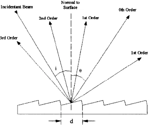
For a plane grating共Fig. 1兲 with i and the incidence and diffraction angles of light, respectively, with respect to the surface normal of the grating, diffracted quasimonochro-matic light with wavelengthin the mth order will be given by2,8
d共sin⫾sin i兲⫽m, 共1兲
where d is the distance between adjacent grooves on the grating surface. In the equation, a positive sign indicates that
and i are located on the same side of the surface normal, otherwise the sign will be negative. In the design, we use the negative sign because and i are on opposite sides of the surface normal. By considering first-order (m⫽1) diffrac-tion, Eq. 共1兲can be rewritten as
a兲Electronic mail: [email protected]
REVIEW OF SCIENTIFIC INSTRUMENTS VOLUME 74, NUMBER 6 JUNE 2003
2973
sin⫽m/d⫹sin i⫽/d⫹g0, 共2兲
where g0is a constant related only to the incidence angle i of
the light on the grating. For a fixed d, the diffracted spectral lines will be distributed in a wavelength window ⌬ corre-sponding to the diffraction angles ranging from1 to2:
sin2⫺sin1⫽共2⫺1兲/d⫽⌬/d. 共3兲
The spectral resolving power R in first order is defined as
R⫽/⌬⫽N, 共4兲
where N is the total number of grooves on the grating. For a typical grating with a groove density of 1200 g/mm and a useful width of 30 mm, R⫽36 000, which will give an ideal wavelength resolution of ⌬⫽0.013 nm at ⫽500 nm. In practical applications, the resolution may not be as high as is expected. To get a rapid spectral measurement by using a CCD array detector, a large number of pixels may be re-quired to cover the entire spectral range with high resolution. For example, in the 200–1000 nm wavelength range, at least 9000 pixels along the spectrum are needed to obtain a reso-lution of 0.1 nm for each pixel with the required minimum area size to produce enough photoelectrons in a high-dynamical 12–16-bit A/D signal-converting range. For a CCD detector with a standard 24⫻24 m2 pixel size, the required total signal-sensing area will be 216 mm long. This is technically unrealistic for CCD design and fabrication. By taking the advantage of a two-dimensional CCD array detec-tor, however, we can solve the problem of folding the spec-trum in space. According to Eq.共3兲, for example, by taking proper grating d values, diffracted light with different wave-lengths will be distributed in the same range of diffraction angles, i.e.,
⌬共sin兲⫽sin2⫺sin1⫽共4⫺3兲/d3⫽共3⫺2兲/d2
⫽共2⫺1兲/d1. 共5兲
For example, three gratings with groove densities of 1200 g/mm (d1⫽833 nm), 600 g/mm (d2⫽1667 nm), and
300 g/mm (d3⫽3333 nm), respectively, can be used.
There-fore, we have three wavelength windows, i.e.,
⌬1⫽2 共300 nm兲⫺1 共150 nm兲⫽150 nm, ⌬2⫽3 共600 nm兲⫺2 共300 nm兲⫽300 nm, ⌬3⫽4 共1200 nm兲⫺3 共600 nm兲⫽600 nm.
The three windows can be arranged properly in two-dimensional space to cover the entire 150–1200 nm wave-length range in the same diffraction-angle range due to the constant ratios of ⌬1/d1⫽⌬2/d2⫽⌬3/d3. As seen in
Fig. 2共a兲, the three gratings 共each has dimensions of L/3
⫻L), can be put together to form a new plane grating with
the total grating size of L⫻L. In terms of a proper design of
[image:5.612.337.538.47.429.2]the optical system, three spectral-image zones corresponding to the three wavelength windows can be formed on the focal plane of the CCD array detector. The focal plane, consisting of 1024⫻1024 pixels, for example, will be divided into three spectral image zones. Each zone will have about 340⫻1024 pixels. Therefore, the effective measurement area along the wavelength direction will be magnified by three times in the space and will actually have about 3000 pixels in the 150– 1200 nm wavelength range to measure the spectral lines. The average wavelength-to-pixel ratio in the three wavelength
FIG. 1. Plane blazed grating.
FIG. 2. 共a兲Three-grating structure, groove densities of共1兲1200 g/mm,共2兲 600 g/mm,共3兲300 g/mm.共b兲Optical configuration of the system.
2974 Rev. Sci. Instrum., Vol. 74, No. 6, June 2003 Hanet al.
[image:5.612.55.297.53.254.2]windows of ⌬1, ⌬2, and ⌬3 along the pixel direction,
will be about 0.15, 0.3, and 0.6 nm/pixel, respectively. The principle given in this work also can be applied to a grating that can be designed and constructed with more subgratings having different groove d values in order to get higher spec-tral resolution in applications.
III. EXPERIMENT
To test the principle of the method as mentioned earlier, we have used three plane subgratings with groove densities of 1200 g/mm共blazed at 860 nm兲, 600 g/mm共blazed at 400 nm兲, and 300 g/mm 共blazed at 250 nm兲, respectively, to make an integrated plane grating in the experiment. The di-mensions of each subgrating are 30⫻10 mm2 with the grooves parallel to the short side. The total area of the inte-grated grating is 30⫻30 mm2. The designed optical experi-ment system is shown in Fig. 2共b兲.
Light enters the slit having a fixed width of 0.04 mm and is reflected by mirror M1共focal length 110 mm兲. The parallel
light from mirror M1 is incident on the grating at incidence
angle i, about 14.4°. In the incidence plane, the first-order diffracted light in the three wavelength windows, corre-sponding to the three subgratings with different groove d values, is distributed in three zones with the same diffraction angles, as indicated by Eq.共5兲. According to Eqs.共1兲and共5兲, this diffraction light window (⌬⫽2⫺1) is equal to about
12.1°. The spectrum of the quasimonochromatic light is di-vided into three parts along the direction perpendicular to the incident plane. For the subgratings arranged as shown in Fig. 2共a兲, those in the upper, middle, and low positions will dif-fract toward mirror M2quasimonochromatic light distributed
in the 150–300, 300– 600, and 600–1200 nm wavelength ranges with dispersions of about 7.5, 15, and 30 nm/mm, respectively. Toroidal mirror M2, with the same focal length
as M1 in the direction parallel to the incidence plane, is used
to reflect and form the spectral image on the focal plane of the CCD array detector. In the direction perpendicular to the incidence plane, the focal length of M2 is about 550 mm. An
advanced Apogee AP6共UV兲camera with a two-dimensional Si-based CCD array detector was used.7 The CCD detector has 1024⫻1024 pixels with a pixel size of 24⫻24 m2. Therefore, the total photoelectron sensing area is equal to about 25⫻25 mm2 and has a 14-bit A/D signal converting capability. The speed for measuring the optical signal in the entire spectral range can be adjusted and controlled by the camera shutter through software according to the signal in-tensity. The minimum time for capturing a full frame of the spectral image on the focal plane of the CCD detector will be 0.01 s. Two high-pass filters with wavelength-cut edges at 300 and 580 nm were placed in front of the two subgratings
共600 and 300 g/mm, respectively兲 to cut off second-order diffracted light. After taking a spectral image, the digitized spectral data were transferred immediately from the camera to the computer, saved, and were analyzed further in the experiment.
IV. RESULTS AND DISCUSSION
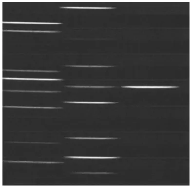
The typical spectral lines of a Hg lamp were measured by the system. An image of these spectral lines taken by the CCD camera is shown in Fig. 3. It can be seen clearly that there are three subspectral regions in its image window cor-responding to the three subgratings with different groove d values. From left to right in Fig. 3, the wavelength is distrib-uted in the 600–1200, 300– 600, and 150–300 nm ranges, respectively. For the Si-based detector used in this instru-ment, wavelengths below 200 nm and above 1000 nm will not be measured. Due to imperfections in optical compo-nents, and also according to Eqs. 共1兲–共5兲, pixel position is not linear in wavelength in the two-dimensional image space. By using a mathematical pattern analysis method, therefore, multiple mathematical polynomial functions have been used to fit the spectral lines to the pixel positions in those three sub-spectral regions. For the best fitting to the data, the wavelength is the function of the pixel position x in the subwavelength region as
共x兲⫽a0⫹a1x⫹a2x2⫹a3x3. 共6兲
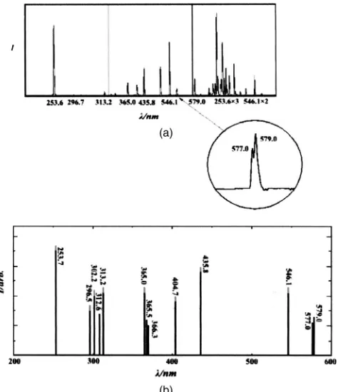
The advantage using the two-dimensional CCD array de-tector is that we can do spectral calibration on every pixel. As mentioned earlier, in each subregion of the CCD focal plane, there are 340⫻1024 pixels. This implies that there are 340 spectral lines, i.e.,(x)1, (x)2...(x)340along the di-rection parallel to the incidence plane with different sets of coefficient an(n⫽0,1,2,3) according to Eq. 共6兲. We can in-dividually calibrate each such line, and then take the average of the line intensity I() with the same wavelength by add-ing them to increase the data accuracy. To avoid the error, a small part of data in the cross subspectral region was dis-carded. The calibrated spectral curves are shown in Fig. 4共a兲. Afterwards, the polynomial functions of the fitting curve, as shown in Fig. 5, were saved in the program and used in the experiment. The comparison between the measured and stan-dard spectral lines of the Hg lamp is shown in Figs. 4共a兲and 4共b兲.
[image:6.612.339.534.52.243.2]The entrance slit with fixed width of 0.04 mm will be imaged with the same width showing on the focal plane of
FIG. 3. Hg-lamp spectrum from the two-dimensional CCD array detector.
2975
the detector. This width covers about two pixels. In the ideal situation, therefore, the highest spectral resolution will be equal to about 0.3, 0.6, and 1.2 nm in the 150–300, 300– 600, and 600–1200 nm wavelength ranges, respectively. The spectral resolution may be not uniform along the pixel posi-tions away from the center of the spectrum due to optical limitations of the design. In practical applications, however, it can be tested to see, as in Fig. 4, that the two 577 and 579 nm characteristic Hg spectral lines, located near at the edge of the 300– 600 nm spectral window, are clearly resolved. This indicates that the spectral resolution in the region is
better than 1.0 nm and agrees well with design expectations. The principle and method given in this work can be applied to optical systems with longer focal lengths and more sub-gratings to achieve higher spectral resolution.
The method studied in this work has been applied to a spectroscopic ellipsometric system in which the polarizer and analyzer are rotated and fixed, respectively. The ellipti-cally polarized light containing the optical information from the sample passes through the fixed analyzer and then enters the spectrometer system with the CCD array camera as de-signed in this work. Instead of mechanically scanning the wavelength in each operation step, the spectral data in the entire wavelength range at each azimuth angle of the polar-izer can be measured in less than 0.1 s with good signal-to-noise ratio. The complex dielectric function of a gold sample was measured, for example, showing results in good agree-ment with those measured by other methods. We will discuss the method in more detail elsewhere.
In this work, we have designed a new type of spectrom-eter system by using a two-dimensional Si-based CCD array detector and an integrated grating consisting of three sub-gratings. The effective spectral area for measuringe spectral data in the limited focal plane of the detector is magnified by a factor of 3. The digitized spectral image in the 200–1000 nm wavelength range can be quickly measured without any mechanical moving part in the system. The nonlinear rela-tionship between the CCD pixel position and wavelength has been studied with multiple polynomial functions in the cali-bration procedure to fit the data by using the mathematical pattern analysis method. The principle can be applied to sys-tems for doing rapid spectroscopic data analysis in many types of photoelectronic experimental research.
ACKNOWLEDGMENTS
This work is supported by the MOST and NSF 共No. 69878003兲of China.
1R. Ramaswami and K. N. Sivarajan, Optical Networks: A Practical
Per-spective共Morgan Kaufmann, San Francisco, 1998兲.
2M. V. Klein and T. E. Furtak, Optics, 2nd ed.共Wiley, New York, 1986兲,
Chap. 5.
3
A. J. Peter, Proc. SPIE 1937, 234共1993兲.
4T. L. Helg, T. H. Barnes, and T. G. Haskell, Opt. Lasers Eng. 29, 413
共1998兲.
5G. E. Smith, Nucl. Instrum. Methods Phys. Res. A 471, 1共2001兲. 6
Monospec 27, Genesis Laboratory Systems, Inc., 2527 Foresight Circle, Grand Junction, CO 81505-1007.
7Apogee Instruments, Inc., 11760 Atwood Rd., Auburn, CA 95603. 8M. Born and E. Wolf, Principles of Optics, 6th ed.共Pergamon, New York,
[image:7.612.58.295.52.327.2]1980兲, Chap. 8. FIG. 4. 共a兲Measured Hg-lamp spectrum.共b兲Standard Hg-lamp spectrum.
FIG. 5. Calibrated spectral curves in the three spectral ranges.
2976 Rev. Sci. Instrum., Vol. 74, No. 6, June 2003 Hanet al.
[image:7.612.53.298.519.613.2]