Rochester Institute of Technology
RIT Scholar Works
Theses Thesis/Dissertation Collections
2006
Development of deep submicron CMOS process
for fabrication of high performance 0.25 nm
transistors
Michael Aquilino
Follow this and additional works at:http://scholarworks.rit.edu/theses
This Thesis is brought to you for free and open access by the Thesis/Dissertation Collections at RIT Scholar Works. It has been accepted for inclusion in Theses by an authorized administrator of RIT Scholar Works. For more information, please [email protected].
Recommended Citation
Development of a Deep-Submicron CMOS Process for
Fabrication of High Performance 0.25 µm Transistors
By
Michael V. Aquilino
A Thesis Submitted
in Partial Fulfillment
of the Requirements for the Degree of
Approved by:
Professor:
Professor:
Professor:
Master of Science
m
Microelectronic Engineering
Dr. Lynn F. FuIler (Thesis Advisor)
Dr.'�� Committee Member)
Dr. Santosh K. Kurinec (thesis Committee Member)
DEPARTMENT OF MICROELECTRONIC ENGINEERING
COLLEGE OF ENGINEERING
ROCHESTER INSTITUTE OF TECHNOLOGY
ROCHESTER, NY
Development of a Deep-Submicron CMOS Process for
Fabrication of High Performance 0.25 µm Transistors
By,
Michael V. Aquilino
I, Michael V. Aquilino, hereby grant permission to the Wallace Library, of the Rochester Institute of Technology, to reproduce this document in whole or in part, with the knowledge that any reproduction will not be for commercial use or profit.
I dedicate this master’s thesis to my family: Michael Sr.,
Giovanna, Joanne, Melissa, Jamie, Joshua and Rachel, whom
Acknowledgments
I would like to thank Dr. Lynn F. Fuller, my thesis advisor, for his continuous support, encouragement, and trust throughout my 6 years at RIT. I have enjoyed being your teaching assistant for 6 classes over the last 2 years as well as collaborating on academic and industry research projects. The work presented in this thesis would not be possible without your help. You are truly the rock which MicroE is built on and I will always look back with fond memories of my time here working with you.
I would like to thank Dr. Hirschman and Dr. Kurinec, my other thesis committee members, for their expertise and financial support in helping me complete this thesis. It’s a great accomplishment that we can now say the Microelectronic Engineering Department has made 0.25 µm CMOS Transistors and is a testament to your excellence in teaching and the quality of our cleanroom.
All of the other Microelectronic Engineering faculty & staff are thanked for teaching me something new every day, whether it be in a lecture, a lab, or everyday interaction. This includes: Dr. Sean Rommel, Dr. Michael Jackson, Dr. Bruce Smith, Dr. Robert Pearson, Prof. Dale Ewbank and Sara Widlund.
The staff of the Semiconductor & Microsystems Fabrication Laboratory at RIT is thanked for their technical expertise and assistance in keeping all of the tools used for this work up and running. Specifically, I would like to thank Bruce Tolleson, whom spent countless hours helping me bring up the Westech 372 wafer polisher for CMP, continuous support on the DryTek Quad RIE and LPCVD system. You are the best technician we have and it’s been a pleasure working with you. I would also like to thank David Yackoff for his help with the Canon Stepper and spending 3 days straight helping to calibrate the two Rapid Thermal Processors which are now running the best they have ever run. Additionally I thank: Sean O’Brien, Scott Blondell, Tom Grimsley, Rich Battaglia and John Nash.
Abstract
An advanced process for fabrication of 0.25 µm CMOS transistors has been
demonstrated. This process is designed for transistors with Lpoly = 0.25 µm and
Leffective = 0.2 um on 150 mm (6”) silicon wafers. Devices with Leffective of 0.2 um and
smaller have been tested and found operational. A 0.25 um NMOS transistor with
drain current of 177 µA/µm at VG=VD=2.5 V and a PMOS transistor with drain
current of 131 µA/µm at VG=VD=-2.5 V are reported. The threshold voltages are
1.0 V for the NMOS and -0.735 V for the PMOS transistors. These 0.25 um NMOS
and PMOS are the smallest transistors ever fabricated at RIT.
Many processes have been integrated to produce the final CMOS devices,
including: 50 Å gate oxide with N2O, shallow trench isolation by chemical
mechanical planarization (CMP), dual doped polysilicon gates for surface channel
devices, ultra-shallow low doped source/drain extensions using low energy As and
BF2 ions, rapid thermal dopant activation, Si3N4 sidewall spacers, TiSi2 salicide
source/drain contacts and gates, uniformly doped twin wells, contact cut RIE and 2
Table of Contents
Abstract... v
Table of Contents... vi
List of Figures ... ix
List of Tables ... xi
List of Abbreviations ... xii
Chapter 1 Introduction... 1
Chapter 2 Device Design... 2
(2.1) Scaling Trends... 2
(2.2) Transistor physics... 3
(2.3) Short Channel Effects... 6
(2.4) NTRS scaling parameters... 10
(2.4.1) 50 Å Gate Oxide with Nitrogen Incorporation ... 11
(2.4.2) Channel Doping ... 12
(2.4.3) Supply Voltage and Sub-threshold Swing ... 14
(2.4.4) Low Doped Source/Drain Extensions... 15
(2.4.5) Source/Drain Contact... 17
(2.4.6) Titanium Silicide... 18
Chapter 3 Process Details... 21
(3.1) Process Flow... 21
(Step 1) Scribe... 22
(Step 2) Four Point Probe... 23
(Step 3) RCA Clean ... 24
(Step 4) Pad Oxidation ... 26
(Step 5) LPCVD Silicon Nitride ... 27
(Step 6) Photo 1: Active (STI) ... 28
(Step 7) Shallow Trench Reactive Ion Etch... 31
(Step 8) PR Strip ... 33
(Step 9) RCA Clean ... 33
(Step 10) Liner Oxidation ... 33
(Step 11) Photo 2: N-Well... 34
(Step 12) N- Well Implant... 37
(Step 13) PR Strip ... 38
(Step 14) Photo 3: P-Well ... 38
(Step 15) P-Well Implant ... 39
(Step 16) PR Strip ... 40
(Step 17) RCA Clean ... 40
(Step 18) PECVD TEOS SiO2 Trench Fill ... 40
(Step 19) Shallow Trench CMP ... 41
(Step 20) Post-CMP Clean ... 43
(Step 21) Decontamination Clean ... 44
(Step 22) RCA Clean ... 44
(Step 23) TEOS Densification ... 44
(Step 24) Hot Phosphoric Nitride Etch ... 45
(Step 26) BOE Etch... 47
(Step 27) RCA Clean ... 48
(Step 28) 50 Å Gate Oxidation... 49
(Step 29) LPCVD Polysilicon... 51
(Step 30) Photo 4: Poly ... 52
(Step 31) Resist Trim Gates ... 54
(Step 32) Poly Gate RIE... 55
(Step 33) PR Strip ... 56
(Step 34) RCA Clean ... 56
(Step 35) Poly Re-Ox ... 57
(Step 36) Photo 5: N-LDD ... 58
(Step 37) N-LDD Implant ... 59
(Step 38) PR Strip ... 61
(Step 39) Photo 6: P-LDD... 61
(Step 40) P-LDD Implant... 62
(Step 41) PR Strip ... 64
(Step 42) RCA Clean ... 64
(Step 43) LPCVD Spacer Nitride... 64
(Step 44) Si3N4 Sidewall Spacer RIE ... 66
(Step 45) Photo 7: N+ S/D ... 67
(Step 46) N+ S/D Implant... 68
(Step 47) PR Strip ... 70
(Step 48) Photo 8: P+ S/D... 70
(Step 49) P+ S/D Implant... 71
(Step 50) PR Strip ... 73
(Step 51) RCA Clean ... 73
(Step 52) RTP S/D Anneal... 73
(Step 53) Oxide Etch... 75
(Step 54) Titanium Deposition... 76
(Step 55) C49 Phase TiSi2 – RTP-1 ... 77
(Step 56) Un-reacted Ti Etch ... 79
(Step 57) C54 Phase TiSi2 – RTP-2 ... 80
(Step 58) PECVD TEOS ILD-0 Deposition ... 80
(Step 59) Photo 9: Contact Cut ... 82
(Step 60) Plasma Etch ... 83
(Step 61) PR Strip ... 85
(Step 62) Metal 1 Deposition ... 85
(Step 63) Photo 10: Metal 1 ... 86
(Step 64) Metal 1 Plasma Etch... 88
(Step 65) PR Strip ... 89
(Step 66) PECVD TEOS ILD-1 Deposition ... 90
(Step 67) Backend CMP... 91
(Step 68) Photo 11: Via... 91
(Step 69) Plasma Etch Via ... 92
(Step 70) PR Strip ... 93
(Step 72) Photo 12: Metal 2 ... 94
(Step 73) Metal 2 Plasma Etch... 95
(Step 74) PR Strip ... 96
(Step 75) Sinter ... 96
(3.2) Stepper Jobs... 98
(3.3) Test Chip ... 99
Chapter 4 Unit Process Development... 102
(4.1) Shallow Trench Isolation... 103
(4.2) TEOS SiO2 CMP ... 109
(4.3) Photoresist Trim for 0.25 µm Lines ... 113
(4.4) Poly Gate Reactive Ion Etch ... 116
(4.5) Si3N4 Sidewall Spacer RIE... 119
(4.6) Titanium Silicide ... 121
(4.7) Contact Cut RIE ... 123
(4.8) Metal Fill of Contact Cuts ... 125
Chapter 5 Results/Analysis... 126
(5.1) NMOS ID-VD (Family of Curves) ... 127
(5.2) NMOS ID-VG ... 129
(5.3) NMOS Sub-threshold ID-VG... 130
(5.4) PMOS ID-VD (Family of Curves) ... 132
(5.5) PMOS ID-VG... 133
(5.6) PMOS Sub-threshold ID-VG ... 134
(5.7) VT Roll-off... 136
(5.8) Effective Channel Length Extraction ... 137
(5.9) P+ Poly C-V ... 140
(5.10) N+ Poly C-V ... 141
Chapter 6 Conclusion ... 143
List of Figures
Figure 2-1: Technology, features size and transistor cost vs. year ... 2
Figure 2-2: NMOS Cross Section in Inversion Mode ... 3
Figure 2-3: Drain Induced Energy Barrier Lowering ... 7
Figure 2-4: Channel Length Modulation ... 7
Figure 2-5: Influence of DIBL on Sub-threshold and VT... 8
Figure 2-6: Threshold Voltage Roll-Off ... 9
Figure 2-7: Source/Drain Punch Through at High Drain Bias ... 9
Figure 2-8: Scaling Guidelines as a Function of Gate Length ... 10
Figure 2-9: Transistor Schematic with Parasitic Resistances ... 19
Figure 3-1: RCA Clean Process... 24
Figure 3-2: Starting Wafer ... 25
Figure 3-3: 500 Å Pad Oxide ... 26
Figure 3-4: STI LPCVD Nitride Deposition... 27
Figure 3-5: Level 1 Lithography - Active... 28
Figure 3-6: SSI Track Coat/Develop Recipes... 30
Figure 3-7: STI Trench Etch ... 31
Figure 3-8: Shallow Trench Liner Oxide... 34
Figure 3-9: Level 2 Lithography - N-Well ... 35
Figure 3-10: SSI Track Coatmtl/Devmtl Recipes... 36
Figure 3-11: N-Well Implant ... 37
Figure 3-12: Level 3 Lithography - P-Well ... 38
Figure 3-13: P-Well Implant... 39
Figure 3-14: PECVD TEOS Shallow Trench Fill... 41
Figure 3-15: Shallow Trench Isolation After CMP ... 42
Figure 3-16: Hot Phosphoric Nitride Strip... 46
Figure 3-17: Twin Well Drive In... 47
Figure 3-18: Pad Oxide Etch Prior to Gate Oxidation... 48
Figure 3-19: 50 Å Gate Oxide Growth ... 50
Figure 3-20: 2000 Å Polysilicon Deposition by LPCVD ... 52
Figure 3-21: Level 4 Lithography – Poly ... 53
Figure 3-22: 0.25 µm Photoresist Trimming ... 55
Figure 3-23: Poly Gate RIE ... 56
Figure 3-24: Poly Re-Ox Crossection... 57
Figure 3-25: Level 5 Lithography - NLDD ... 59
Figure 3-26: N-LDD Implant... 60
Figure 3-27: Level 6 Lithography - PLDD ... 62
Figure 3-28: P-LDD Implant ... 63
Figure 3-29: LPCVD Spacer Nitride Deposition... 65
Figure 3-30: Sidewall Spacer Reactive Ion Etch ... 66
Figure 3-31: Level 7 Lithography – N+ S/D ... 68
Figure 3-32: N+ S/D Implant... 69
Figure 3-33: Level 8 Lithography – P+ S/D... 71
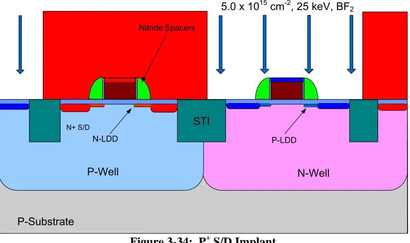
Figure 3-34: P+ S/D Implant ... 72
Figure 3-36: Pre-Titanium Deposition Oxide Etch... 76
Figure 3-37: 1000 Å Titanium Deposition for TiSi2 Process... 77
Figure 3-38: C49 Phase Titanium Silicide after RTP-1... 78
Figure 3-39: Etch Un-reacted Titanium after TiSi2 Formation... 79
Figure 3-40: PECVD TEOS ILD-0 Deposition... 81
Figure 3-41: Level 9 Lithography – Contact Cut... 82
Figure 3-42: Contact Cut Plasma Etch... 84
Figure 3-43: Metal 1 Aluminum Deposition ... 86
Figure 3-44: Level 10 Lithography – Metal 1 ... 87
Figure 3-45: Metal 1 Etch ... 89
Figure 3-46: ILD-1 PEDVD TEOS Deposition... 90
Figure 3-47: Backend CMP of ILD-1... 91
Figure 3-48: Level 11 Lithography - Via... 92
Figure 3-49: Via Plasma Etch ... 93
Figure 3-50: Metal 2 Aluminum Deposition ... 94
Figure 3-51: Level 12 Lithography – Metal 2 ... 95
Figure 3-52: Metal 2 Plasma Etch ... 96
Figure 3-53: Final CMOS Crossection after Sinter ... 97
Figure 3-54: Mentor Graphics Layout of Test Chip ... 99
Figure 4-1: STI vs. LOCOS for Isolation Technology ... 103
Figure 4-2: Submicron Shallow Trenches after RIE... 104
Figure 4-3: Photoresist Damage Causing Footing at Bottom of Trench ... 105
Figure 4-4: Shallow Trench RIE Characterization Results... 105
Figure 4-5: TEOS Filling of Shallow Trenches... 107
Figure 4-6: Shallow Trench Isolation after CMP of TEOS SiO2... 108
Figure 4-7: Oxide CMP Removal Rate vs. Wafer Pressure... 110
Figure 4-8: Nitride CMP Removal Rate vs. Wafer Pressure ... 111
Figure 4-9: Pattern Density Dependence on CMP... 111
Figure 4-10: 0.454 µm Photoresist Line Before Resist Trimming ... 114
Figure 4-11: 0.2 µm Photoresist Line After Resist Trimming... 114
Figure 4-12: SEM Micrograph of 0.25 µm Poly Gate... 118
Figure 4-13: 0.25 µm Ring Oscillator with Nitride Spacers... 119
Figure 4-14: SEM Crossection of Nitride Sidewall Spacer on 0.25 µm Poly Gate. 120 Figure 4-15: SEM Micrograph of Submicron Contact Cuts... 123
Figure 4-16: SEM Micrograph of 0.5 µm Contact Cut... 124
Figure 4-17: Contact Cut RIE Characterization Results... 124
Figure 4-18: Submicron Contact Cuts Filled with Aluminum... 125
Figure 4-19: 0.5 µm Contact Cut filled with 4000 A of Aluminum ... 125
Figure 5-1: ID-VD Family of Curves for 0.25 µm NMOS Transistor... 127
Figure 5-2: ID-VD Threshold Voltage Sweep of 0.25 µm NMOS Transistor ... 129
Figure 5-3: ID-VG Sub-threshold for 0.25 µm NMOS Transistor ... 130
Figure 5-4: NMOS Drain Reverse Bias Leakage ... 131
Figure 5-5: ID-VD Family of Curves for 0.25 µm PMOS Transistor ... 132
Figure 5-6: ID-VG Threshold Voltage Sweep for 0.25 µm PMOS Transistor... 133
Figure 5-7: ID-VG Sub-threshold for 0.25 µm PMOS Transistor... 134
Figure 5-9: Transistor with Source/Drain Series Resistance Equivalent Circuit... 137
Figure 5-10: NMOS Effective Channel Length and RSD Extraction ... 138
Figure 5-11: PMOS Effective Channel Length and RSD Extraction... 139
Figure 5-12: CV Analysis for 48 Å EOT P+ Poly Capacitors... 140
Figure 5-13: CV Analysis for 58 Å EOT N+ Poly Capacitors... 141
List of Tables
Table 2-1: NTRS Scaling Parameters for 0.25 µm Transistors ... 10Table 2-2: Summary of Channel Doping Parameters ... 12
Table 2-3: NTRS Guidelines for LDD Scaling ... 15
Table 2-4: NTRS Guidelines for Source/Drain Contact Scaling ... 17
Table 2-5: Reduction in IDSAT Due to Parasitic Resistance... 20
Table 3-1: Wafer Identification ... 22
Table 3-2: Starting Wafer Information ... 23
Table 3-3: 500 Å Pad Oxide Recipe ... 26
Table 3-4: FACNIT810 Recipe ... 27
Table 3-5: Level 1 Lithography Parameters ... 30
Table 3-6: STI Etch Recipe... 32
Table 3-7: 6” Hard Ash Receipe... 33
Table 3-8: Level 2 Lithography Parameters ... 36
Table 3-9: Level 3 Lithography Parameters ... 39
Table 3-10: P5000 TEOS Recipe... 41
Table 3-11: STI CMP Recipe ... 43
Table 3-12: Recipe 206 TEOS Densification ... 45
Table 3-13: Twin Well Drive In Recipe ... 47
Table 3-14: 50 Å Gate Oxide w/N2O Recipe... 50
Table 3-15: FACPOLY610 Recipe... 52
Table 3-16: Level 4 Lithography Parameters ... 53
Table 3-17: 100 Å Poly Re-Ox Recipe ... 58
Table 3-18: Level 5 Lithography Parameters ... 59
Table 3-19: Level 6 Lithography Parameters ... 62
Table 3-20: LPCVD Spacer Nitride Recipe... 65
Table 3-21: Nitride Spacer Etch Recipe ... 67
Table 3-22: Level 7 Lithography Parameters ... 68
Table 3-23: Level 8 Lithography Parameters ... 71
Table 3-24: RTP S/D Anneal Recipe... 75
Table 3-25: Titanium Sputter Deposition Process ... 77
Table 3-26: C49 Phase Titanium Silicide Recipe ... 78
Table 3-27: C54 Phase Titanium Silicide Recipe ... 80
Table 3-28: 3000 Å ILD-0 P5000 TEOS Deposition Recipe ... 82
Table 3-29: Level 9 Lithography Parameters ... 83
Table 3-30: Contact Cut RIE Recipe ... 85
Table 3-31: Aluminum Metal 1 Sputter Deposition Process ... 86
Table 3-33: Recipe 101 – Sinter Details ... 97
Table 3-34: 0.25 µm Test Chip Design Layers... 100
Table 4-1: CMP Characterization Results ... 110
Table 4-2: LAM490 Resist Trim Process ... 113
Table 4-3: Photoresist Trimming Results ... 113
Table 4-4: Polysilicon RIE Recipe ... 117
Table 4-5: Titanium Silicide Properties... 121
Table 4-6: TiSi2 Sheet Resistance Results ... 122
Table 5-1: 0.25 µm NMOS Transistor Electrical Results... 131
Table 5-2: 0.25 µm PMOS Transistor Electrical Results ... 135
List of Abbreviations
CMOS – Complementary Metal Oxide Semiconductor NMOS – N-Channel Metal Oxide Semiconductor PMOS – P-Channel Metal Oxide Semiconductor IC – Integrated Circuit
VLSI – Very Large System Integration
NTRS – National Technology Roadmap for Semiconductors DIBL – Drain Induced Barrier Lowering
VT – Threshold Voltage
EOT – Equivalent Oxide Thickness SS – Sub-threshold Swing
XJ – Junction Depth RS – Sheet Resistance DOF – Depth of Focus CD – Critical Dimension
VASE – Variable Angle Spectroscopic Ellipsometer STI – Shallow Trench Isolation
CMP – Chemical Mechanical Planarization SALICIDE – Self Aligned Silicide
RIE – Reactive Ion Etch LDD – Low Doped Drain SDE – Source Drain Extension
LPCVD – Low Pressure Chemical Vapor Deposition PECVD – Plasma Enhanced Chemical Vapor Deposition MERIE- Magnetically Enhanced Reactive Ion Etch RTP – Rapid Thermal Processor
TED – Transient Enhanced Diffusion TEOS – Tetra Ethyl Ortho Silicate Oxide – SiO2
Nitride – Si3N4
Poly – Polysilicon
ILD – Inter-level Dielectric
Chapter 1
Introduction
For over twenty years the Microelectronic Engineering Department at RIT has
strived to continue the semiconductor industry trend of fabricating smaller and faster
transistors. RIT is currently supporting 0.5 µm, 1.0 µm and 2.0 µm CMOS
technologies that are fabricated daily in a student run factory. Students improve
existing processes for current CMOS lines and develop new advanced processes that
can be integrated into future technologies. Until this work, the smallest transistor
fabricated in the Semiconductor and Microsystems Fabrication Laboratory (SMFL) at
RIT is an NMOS device with Lpoly = 0.5 µm and Leff = 0.4 µm, completed in May
2004 by the author.
The goal of this work is to develop a deep-submicron CMOS process to
fabricate transistors with Lpoly = 0.25 µm on 150 mm (6”) silicon wafers. The device
technology includes: 50 Å gate oxide with N2O, shallow trench isolation by chemical
mechanical planarization (CMP), dual doped polysilicon gates for surface channel
devices, ultra-shallow low doped source/drain extensions using low energy As and
BF2 ions, rapid thermal dopant activation, Si3N4 sidewall spacers, TiSi2 salicide
source/drain contacts and gates, uniformly doped twin wells, 2 level aluminum
metallization and is designed to operate at a supply voltage of up to 2.5 V with a
threshold voltage of ± 0.5 V. This technology will expose students to advanced
Chapter 2
Device Design
(2.1) Scaling Trends
Gordon Moore, the co-founder of Intel Corporation, predicted the transistor
density on an integrated circuit (IC) would double every 18-24 months. [1] This
became known as “Moore’s Law” and has been a driving force in the scaling of
transistors even today. The advancement in transistor technology has allowed
transistors with gate lengths of 65 nm to be produced today compared to 10 µm in
1971. This is a 150x reduction in gate length which results in a 36,000x increase in
switching speed and a 60,000x increase in number of transistors on an IC. Figure 2-1
is a summary of industry scaling trends of technology feature size, transistor gate
length and transistor cost over the last 35 years.
(2.2) Transistor physics
A transistor is a four terminal active device consisting of a gate, source, drain,
and body. An NMOS device has an n+ source/drain region diffused into a p-type
body. To turn the device on, a positive voltage above the threshold voltage, VT, is
applied to the gate to repel positively charged holes at the surface. The gate is
insulated from the body by a thin dielectric layer. This creates a surface region
depleted of holes and exposes the negatively ionized p-type acceptor atoms. This is
known as bulk charge,QB, and supports electric field lines emanating from the
positive gate charge, QG. The remaining electric field lines terminate on electrons
that diffuse from the source, known as inversion charge,QI. The sum of the
negativeQBand negative QI make up the total positiveQG. The source and body are
grounded and a positive voltage is applied to the drain which attracts the inversion
charge. This inversion charge moves from source to drain and becomes the current
flowing through the device. Figure 2-2 is a schematic of an NMOS transistor with its
terminal voltages labeled. An analogous analysis can be made for a PMOS transistor.
Equation 2-1 is the classical derivation for the drain current of an NMOS transistor
calculated by integrating the inversion charge along the channel. [4]
Equation 2-1
Q
V
dV
L
W
I
n nVD
VS
DS
=
∫
µ
(
)
The resulting equation for the source to drain current in the linear region of
operation is shown in Equation 2-2. In the linear region, the current increases
approximately linear with increasing drain voltage. Also, the current is dependent on
majority carrier mobility, oxide capacitance per unit area, width to length ratio and
the overdrive of the gate voltage above the threshold voltage.
Equation 2-2
(
)
( )
22
'
DS DS T GS OX DSV
V
V
V
L
W
C
I
LIN=
µ
−
−
As the drain voltage increases to its saturation voltage (VDS-SAT = VGS – VT),
the transistor enters the saturation region of operation. In this region the current
increases with the square of the (VGS-VT) overdrive. The resulting equation for the
source to drain current in the saturation region of operation is shown in Equation 2-3.
In a long channel transistor, the drain current is independent of the drain voltage. In
other words, the gate has full control of the current conducted through the channel.
Equation 2-3
(
)
2
2
'
GS TOX
DS
V
V
L
W
C
I
SAT=
µ
−
The threshold voltage for the NMOS transistor is shown in Equation 2-4. The three
main components of the threshold voltage is the flat band voltage, bulk potential and
Equation 2-4
'
4
2
OX B a s B FB TC
N
q
V
V
=
+
Ψ
+
ε
Ψ
Equation 2-5
'
'
ox ox MS FBC
Q
V
=
Φ
−
Equation 2-6
⎟
⎠
⎞
⎜
⎝
⎛
=
Ψ
i a Bn
N
q
kT
ln
The flat band voltage, VFB, shown in Equation 2-5, is dependent on the
metal-semiconductor work function, ΦMS, and the charge in the gate oxide, QOX’, divided by
the oxide capacitance, COX’. ΦMS is dependent on the metal Fermi potential and the
type of semiconductor. For an NMOS transistor with N+ poly or Aluminum, ΦMS is
typically a negative voltage. For a PMOS transistor with N+ poly, ΦMS is typically a
negative voltage, but with P+ poly ΦMS is typically a positive voltage. The bulk
potential, ΨB, is dependent on the thermal voltage and the natural log of the doping
concentration, Na, divided by the intrinsic carrier concentration, ni. For an NMOS
device, ΨB is positive, for a PMOS device, ΨB is negative. The third term in the VT
equation is the voltage drop across the oxide which depends on the oxide capacitance
and the doping and type of the substrate. For NMOS transistors this voltage is
typically positive while typically negative for PMOS transistors. To turn the
transistor on, the gate voltage must overcome the flat band voltage, a voltage drop
across the gate oxide and a voltage drop across the semiconductor, which involves
(2.3) Short Channel Effects
In devices with long gate lengths, the gate is the primary terminal in
supporting the inversion charge in the channel. There is a depletion region which
extends from the source and drain into the channel caused by the reverse biased p-n
junctions they make with the body. The positively ionized donor atoms on the n+
drain side of the body-drain p-n+ junction also allows for some support of inversion
charge in the channel. For large devices, the contribution of the drain in controlling
the inversion layer in the channel is much smaller compared to the gate. However, as
devices are scaled down in length, the drain has a larger percentage contribution in
supporting inversion charge in the channel. This effect is known as “charge sharing”
and effectively reduces the control the gate has over the channel of the device. The
off-state leakage current will increase since the gate doesn’t have full control of
turning the device off. The solution to this problem is to scale physical parameters of
the device to increase the control of the gate. “Gate control” is the most important
concept in the physics of a transistor for proper operation in the on and off state.
Figure 2-3 shows the surface potential in the channel of an NMOS transistor
versus position from the source to drain. It can be seen as the drain bias is increased,
the surface potential in the drain region increases. Additionally, it can be seen the
surface potential also increases into the drain side of the channel. This results in
lowering of the thermal barrier that is supposed to be fully controlled by the gate.
The reduction in surface potential, or energy barrier, is known as Drain Induced
Barrier Lowering (DIBL). DIBL manifests itself in multiple ways in electrical
Figure 2-3: Drain Induced Energy Barrier Lowering [5]
The most common short channel effect is noticed in the “family of curves”
ID-VD plot shown in Figure 2-4. In the saturation region of operation the current in
the device should remain constant once the saturation voltage is reached. However, it
is noticed the current increases linearly resulting in a slope to the saturation region.
Using this slope, a line can be projected to the negative x-axis and the reciprocal of
this voltage is known as the Early Voltage, λ, and is in units of V-1. The drain current equations shown in Equation 2-2 and Equation 2-3 are modified by a multiplication
factor of (1+λVDS).
VDS
Another short channel effect is seen on a Log (IDS)-VGS plot shown in Figure
2-5. This is the sub-threshold region of operation where the current increases
exponentially until the device turns on. It can be seen as the drain voltage is
increased to a higher potential the current also increases for voltages below threshold.
This results in a higher off-state current that also shifts the threshold voltage of the
device.
Figure 2-5: Influence of DIBL on Sub-threshold and VT
A common metric of calculating the DIBL is shown in Equation 2-7. By
dividing the change in gate voltage by the change in drain voltage at a specified drain
current, a metric in units of mV/V can be obtained. Ideally, this DIBL number is
minimized, meaning the drain has a small impact on current through the device.
Equation 2-7:
DS GS
V
V
DIBL
∆
∆
=
A third common short channel effect is threshold voltage roll-off shown in
Figure 2-5. At very small gate lengths the threshold voltage decreases compared to a
larger gate length device. At some minimum gate length the threshold voltages for
the NMOS and PMOS can roll-off to 0 V. This means both devices will be on with
∆
VTVDS = 2.0 V
VDS = 0.1 V
VGS
zero gate bias and will cause inoperable CMOS circuits. This effect is caused by
DIBL, as for very small gate length devices, the drain barrier is lowered severely and
charge sharing from the drain causes conduction even at zero gate bias.
NMOS + 0.5 V
- 0.5 V
LGATE
VT
PMOS
Figure 2-6: Threshold Voltage Roll-Off
A fourth short channel effect is source/drain punch through shown in Figure
2-7. At high drain bias in the saturation region of operation in the IDS-VDS plot, the
current rapidly increases. The depletion region extending from the drain into the
channel can eventually get close enough to the depletion region from the source to
cause a reduced energy barrier that will increase the drain current. This will cause
excessive heating in the device and can cause analog circuits to operate incorrectly.
VDS
IDS
(2.4) NTRS scaling parameters
The NTRS Roadmap gives guidelines for scaling physical and electrical
parameters to meet on and off state performance requirements at a particular
technology node. [6] Physical parameters such as oxide thickness, source/drain
junction depth and doping concentration, channel doping profile, and side-wall spacer
length are scaled based upon the gate length, λ. Electrical parameters such as
Sub-threshold swing, DIBL, VDD, VT, and parasitic resistances must be controlled to
achieve the required performance parameters such as ION and IOFF. Some of the
NTRS Roadmap guidelines for poly gate lengths of 0.25 µm are shown in Table 2-1.
ION 600 µA/µm Tox 40 - 50 Å
IOFF 1 nA/µm XJ (shallow LDD) 50 – 100 nm
Log(ION / IOFF) 5.75 decades ND (LDD) 2 - 5 x1018 cm-3
SS 85 mV/decade RS (LDD) 400 – 850 Ωsq
DIBL < 100 mV/V XJ (contact) 135 – 265 nm
VDD 1.8 – 2.5 V ND (contact) > 1x1020 cm-3
| VT | 0.5 V XJ (SSRW channel) 50 – 100 nm
Table 2-1: NTRS Scaling Parameters for 0.25 µm Transistors [6]
A schematic of a transistor cross-section with physical parameters scaled
according to gate length, λ, to achieve the performance parameters is shown in Figure
2-8.
(2.4.1) 50 Å Gate Oxide with Nitrogen Incorporation
The gate oxide in a transistor must be scaled smaller in thickness as the gate
length is scaled smaller in size. This is done to give the gate more control in
switching the device on and off. Another way to look at this is the capacitance
between the gate and the substrate must be increased as devices are scaled, keeping in
mind, capacitance is defined as a change in charge for a given change in voltage. In
high-speed circuits, the transistors are turned on and off billions of times per second.
A high capacitance is desirable because a larger change in charge per change in
voltage is possible so the device can be switched from on (large amount of inversion
charge) to off (no inversion charge) very quickly. A very important detail regarding
an ultra thin gate oxide is that there must be nitrogen incorporated into it. This is
because boron from the p-type poly gate will diffuse easily through a thin oxide layer.
The addition of nitrogen into the oxide film will prevent the boron penetration into
the channel region of the PMOS.
The NTRS Roadmap requires a gate oxide of 40 Å – 50 Å for the 0.25 µm
technology node. [6] This is actually an equivalent oxide thickness (EOT) as poly
depletion effects will cause the electrically extracted accumulation mode oxide
thickness to be larger then the physical thickness of the oxide layer. A 50 Å gate
oxide process is used for RIT’s 0.25 µm Deep-Submicron CMOS process. At this
thickness the gate capacitance is estimated to be greater then 690 nF/cm2 and have an oxide electric field of 4 MV/cm at 2.0 V on the gate. This is at the limit of
Fowler-Nordheim tunneling and should not have problems with long term reliability due to
(2.4.2) Channel Doping
As the gate of a transistor is scaled down in length the doping concentration of
the channel must be increased to control short channel effects described in Section
(2.3) The channel region must be doped heavier to reduce the depletion regions from
the source/drain from extending into the channel. This will decrease the control the
drain has on the channel but will also decrease the mobility of the carriers at the
surface since there is more dopant to cause scattering. To do this, the NMOS and
PMOS devices are built in a p-well and n-well, respectively. This is referred to as a
“twin well” process and will allow the doping concentration, junction depth, and
therefore sheet resistance, of each well to be engineered to the proper electrical
parameters. A summary of the channel doping parameters are shown in Table 2-2.
NMOS PMOS NMOS Field PMOS Field
Well Type p n p n
Gate Material N+ Poly P+ Poly N+ Poly P+ Poly Doping Concentration
(cm-3) 6.5x10¹⁷ 5.5x10¹⁷ 6.5x10¹⁷ 5.5x10¹⁷
Junction Depth
(µm) 3 3 3 3
Gate Oxide
(Å) 50 50 4000 4000
Threshold Voltage
(V) + 0.5 V - 0.5 V + 50 V -50 V
Table 2-2: Summary of Channel Doping Parameters
A dual doped poly scheme is used where the NMOS uses N+ poly and the PMOS uses P+ poly. This will allow surface channel transistors to be built since counter-doping of the n-well for the PMOS will not be required to shift the threshold
voltage to a low enough magnitude value. If N+ poly is used for the PMOS, the metal-semiconductor work function is a negative value, which will cause a left shift
voltage for this process is 0.5 V for the NMOS and -0.5 V for the PMOS. A
threshold voltage adjust implant will be needed to make the threshold voltage less
negative and a final value of -0.5 V. To do this, a p-type dopant, boron for example,
would be implanted into the channel to support more inversion charge, and therefore
decrease the amount of gate charge needed to turn the device on. If P+ poly is used
for the PMOS, the metal-semiconductor work function is a positive value, which will
cause a right shift in the threshold voltage to a smaller magnitude negative value. To
shift the threshold voltage to a larger magnitude negative value of -0.5 V, an n-type
dopant, phosphorous for example, would be implanted into the channel to increase the
effective channel concentration at the surface. A larger amount of gate charge will
then be needed to invert the surface and create a hole channel. The P+ poly gate is an advantage for creating surface channel PMOS which will lead to a better gate control
in the turning the device off. As a tradeoff, however, surface channel devices have
lower channel mobility due to increased carrier scattering with the Si/SiO2 surface,
which will cause lower drive currents. This leads to a better off-state control of the
device at the expense of channel mobility.
The junction depths are diffused to around 3 um to ensure the doping is
continuous under all field regions. Also, vertical punch through, between the reverse
biased PMOS drain diode in the n-well and the complimentary doped p-well, will be
eliminated with a large junction depth of the wells. The field oxide is made much
thicker then the gate oxide to ensure the parasitic field transistors that exist between
active devices do not turn on until a voltage much higher then the 1.8 – 2.5 V supply
(2.4.3) Supply Voltage and Sub-threshold Swing
As the oxide thickness is decreased, the supply voltage must be decreased so
the oxide doesn’t break down. Also, the supply voltage must be decreased to reduce
leakage between the reverse-biased drain and body terminal. Since the supply
voltage is decreased, VT must be decreased so that VGS can be sufficiently higher then
VT. This is known as “gate over-drive” and is important since the drive current is
proportional to VGS – VT. The problem that arises is there may not be enough gate
voltage between 0 V and VT to turn the device off. The sub-threshold swing, SS, is a
measure of how much of a change in gate voltage, below VT, is required to change
the off-current in the device by a magnitude of 10. The equation for SS is shown in
Equation 2-8 and has a theoretical limit of 60 mV/decade at room temperature. [3]
Where kT/q is the temperature dependent thermal voltage, CD is the depletion
capacitance which arises from the change in bulk charge for change in gate voltage,
and COX which is the gate oxide capacitance.
Equation 2-8
( )
⎥⎦
⎤
⎢⎣
⎡ +
×
×
=
OX D
C
C
q
kT
SS
ln
10
1
A 0.25 µm device needs a SS of 85 mV/decade to decrease the sub-threshold
current 5.75 decades from on to off given the fact there is 500 mV between 0 V and
VT. It can be seen that as devices scale in length, the supply voltage and VT must be
decreased. Also, the sub-threshold swing must be decreased by decreasing TOX, and
(2.4.4) Low Doped Source/Drain Extensions
The junction depths of the shallow LDD region are made very small so the
depletion region from the gate dominates the depletion region from the drain, thus
giving the gate more control. The LDD implants are self aligned to the poly gate and
are performed after the re-oxidation step which forms a screening oxide of around
100 Å. In industry, the silicon would be implanted with silicon or germanium to
create an amorphous surface layer that low energy implants would be implanted
into. [9] The amorphous layer reduces channeling of the source/drain dopants and
allows for shallower junction depths to be implanted. Also, arsenic is used as the
n-type dopant because it can be implanted to shallow junction depths at a higher
acceleration energy because the projected range is smaller at a given energy
compared to phosphorous. Table 2-3 is a summary of the guidelines from the NTRS
roadmap to meet on and off state performance for a CMOS technology with Lpoly of
0.25 µm.
NTRS Guidelines Range Target
XJ(LDD) 0.4*Lpoly +/- 25% 75 nm – 125 nm 75 nm
RS (LDD) 400 – 850 Ω/sq 400 Ω/sq
ND(LDD) 5.2x10¹⁸ – 2.5 x1018 cm-3 5.2x1018 cm-3
Table 2-3: NTRS Guidelines for LDD Scaling [6]
A range for the junction depth of the shallow LDD is 75 nm – 125 nm. The
target for this process will be 75 nm. The designed source/drain junction depth for
the 0.5 µm NMOS device in [10] was 150 nm. Using basic scaling laws [3],
decreasing the gate length by a factor of 2 requires decreasing the junction depth by a
The target for this process is 400 Ω/sq and an estimated doping concentration of
5.2x1018 cm-3 is required.
To place the peak of the LDD implant at the surface of the silicon, the
projected range must be at least 100 Å, the thickness of the poly re-ox. For BF2, this
energy is 20 keV and for arsenic is 25 keV. 2000 Å of polysilicon is thick enough to
block transmission of BF2 up to 90 keV and arsenic of up to 100 keV.
Transient enhanced diffusion can cause the junction depths to rapidly increase
at temperatures of 670-900°C. [8] Since high temperatures are needed to activate the
dopant and repair damage to the silicon lattice it is necessary to ramp to high
temperature at a fast rate and be able to cool the wafer down quickly as well. Arsenic
is not as susceptible to TED for the n-type LDD and source/drain junctions; however,
boron in the PMOS is much more susceptible to TED and is a concern. Therefore,
the target junction depth and sheet resistance are chosen on the low end so if more
diffusion occurs then is simulated, the devices will still perform well in the on/off
(2.4.5) Source/Drain Contact
As the junction depths of the source/drain contact are made smaller their
parasitic resistances will cause a decrease in drive current. They must therefore be
doped heavier to decrease this resistance. The source/drain contact implants are self
aligned to the poly gate and are offset by the nitride sidewall spacers. They are doped
much heavier then the LDD regions to provide a low resistance path between the
contact cut and LDD in a non-silicided process. This is done by increasing the
implant dose to provide more dopant atoms and increasing the implant energy so a
deeper junction depth will be formed. For a self aligned silicide process, such as this
0.25 µm CMOS process, the deeper junction is required because a portion of the
silicon will be consumed to make the silicide. If silicide accounts for more then half
of the source/drain contact depth, junction leakage will occur and the off-state current
will increase. [8] Table 2-4 is a summary of the guidelines from the NTRS roadmap
to meet on and off state performance for a CMOS technology with Lpoly of 0.25 µm.
NTRS Guidelines Range Target XJ(Contact) 0.8*LPOLY +/- 33% 134 nm – 266 nm 150 nm
ND(Contact) >1x1020 cm-3
Table 2-4: NTRS Guidelines for Source/Drain Contact Scaling [6]
A range for the junction depth of the deeper contact is 134 nm – 266 nm. On average,
the junction depth of the contact is twice that of the shallow LDD. [6] The target
junction depth is therefore 150 nm. The implant energy needed will be on the order
of 30 keV for arsenic and 25 keV for BF2. As stated before, a poly thickness of
2000 Å is thick enough, in conjunction with the poly re-ox thickness, to block
(2.4.6) Titanium Silicide
A self-aligned silicide (SALICIDE) process is used to make very low
resistance contacts in the source/drain/gate regions of the device. For the
source/drain contact regions, the sheet resistance must be made much lower then the
sheet resistance of the LDD so most of the drain voltage is applied across the channel
of the device. For the gate, the lower sheet resistance will allow faster switching
because the gate capacitor will be charged and discharged faster. The NTRS
Roadmap requires the LDD regions cause a maximum reduction in saturation current
of 10%.6 Equation 2-9 will predict the saturation resistance normalized per unit
width,
R
SAT×
W
. [8] Equation 2-10 will predict the resistance of the LDD region as a function of sheet resistance and spacer length normalized per unitwidth,
R
LDD×
W
.W
R
W
R
SAT LDD×
×
must be kept to less then 10%.
Equation 2-9
(
)
T DD sat ox DD SAT
V
V
v
t
V
W
R
OX
×
−
×
×
×
=
×
ε
47
.
0
Equation 2-10
R
LDD×
W
=
R
SLDD×
L
TOTALFor a gate oxide thickness of 50 Å, VDD of 2.0 V, VT of 0.5 V,
v
satof 1x107cm/s,
ε
OX of 3.9×ε
O, andεOof 8.854x10⁻¹⁴ F/cm, an
R
W
SAT
×
value ofFigure 2-9 is a cross section of a transistor with the corresponding parasitic
resistive regions inherent to the device. Below are equations for the calculating the
parasitic resistances shown in Figure 2-9 for a nominal 1 µm wide device. For wider
devices, the individual resistance components will decrease proportional to the width.
Figure 2-9: Transistor Schematic with Parasitic Resistances
Equation 2-11
R
TOTAL=
R
CHANNEL+
R
PARASITICEquation 2-12
R
PARASITIC=
R
EXTENSION+
R
EXTRINSICEquation 2-13
R
EXTENSION=
R
S'
+
R
D'
Equation 2-14
R
EXTRINSIC=
R
S+
R
D+
2
R
CEquation 2-15
Rs
'
×W
=
R
SLDD×
L
spacerEquation 2-16
R
D'
×W
=
R
SLDD×
L
spacerEquation 2-17
Rs
×W
=
R
SSILICIDE×
L
Equation 2-18
R
D ×W
=
R
SSILICIDE×
L
Equation 2-19
2 9
10
2
,
cm
L
W
R
CC
C
=
=
×
Ω
×
−
Table 2-5 below is a summary of the estimation in reduction of drive current when
comparing the parasitic resistance to the channel resistance. It is assumed the length
of the LDD is 0.25 µm, the length of the source/drain contact is 0.75 µm, and length
of the metal contact to silicide is 0.5 µm. Also,
R
SLDD is assumed to be 400 Ω/sqand
R
SSILICIDE is 4 Ω/sq. It can be seen the addition of the source/drain contact andmetal/silicide contact resistances reduce the drive current by 5.1%. The guidelines
from the NTRS Roadmap require <10% reduction in drive current due to the total
parasitic resistance in the device.
W
×
EXTENSION
R
(Ω x µm)
W
×EXTRINSIC
R
(Ω x µm)
W
×
PARASITIC
R
(Ω x µm)
W
×
SAT
R
(Ω x µm)
W
W
× × SAT PARASITICR
R
200 7 207 4108 5.1%
Table 2-5: Reduction in IDSAT Due to Parasitic Resistance
RS and RD can be made to be very low resistance with the use of silicides to decrease
the total parasitic resistance. Titanium silicide (TiSi2) is widely used in 0.25 µm
CMOS processes and is used in Intel’s 0.25 µm CMOS process. [11] The silicide is
Chapter 3
Process Details
This chapter will focus on the details of the 0.25 µm CMOS Process. Section
(3.1) will detail every step in the process flow from bare silicon to multi-level
metallization. To understand the complexity in fabricating even the simplest CMOS
logic circuit, the CMOS inverter, crossectional pictures are included in all relevant
steps of this process. Section (3.2) will contain information on the lithography tool
stepper jobs created for this process. Finally, Section (3.3) will include details on the
test chip created for this process. A layout schematic of the test chip is included to
give the reader a “top-down” perspective of a CMOS IC. These will supplement the
“side-view,” or crossectional, perspective that is presented in Section (3.1).
(3.1) Process Flow
The 0.25 µm CMOS process is the most advanced CMOS process developed
in the Microelectronic Engineering department at RIT. A total of 75 steps will be
described in this section and constitute the main process steps used in fabrication of
the device wafers. A CMOS process flow is very complex and requires careful
planning to ensure a sufficient number of control wafers are included to monitor
critical parameters throughout the fabrication process. Additional details are included
in each step for collecting electrical and physical metrology data to detect any
problems during the fabrication and provide experimental data that can be compared
(Step 1) Scribe
The first step in the process is to scribe each wafer with a lot number and a
unique wafer identification number to distinguish device wafers from control wafers.
By convention, lots run in our student factory begin with the letter F, and are
formatted as FYYMMDD. Where YY is the last 2 digits of the year, MM is the last
2 digits of the month, and DD is the last 2 digits of the Day. Research lots begin with
an R and follow the same format: RYYMMDD. This process is still under
development and improvement so the naming convention chosen is for a research lot
and all wafers are scribed as R050922. Also by convention, wafers that begin with D
are device wafers and wafers that begin with C are control wafers. Device wafers are
intended to see all steps in the process and will be tested for electrical performance
upon completion. Control wafers are typically used as blanket monitor wafers for
film thickness, sheet resistance, junction depth, etch rates, etc. Table 3-1 below
identifies the 10 device wafers and 9 control wafers that will be described in this
process.
Device Wafers Total Wafer ID
Device wafers at end of process 6 D1-D6 Leave behind 2 device wafers after poly etch 2 D7,D8 Leave behind 2 device wafers before gate oxide 2 D9,D10
Monitor Wafers
Blanket Arsenic n-LDD in blanket p-well 1 C1 Blanket Arsenic n-S/D Contact in blanket p-well 1 C2 Blanket BF2 p-LDD in blanket n-well 1 C3
Blanket BF2 p-S/D Contact in blanket n-well 1 C4
NMOS Channel (P-Well) 1 C5
PMOS Channel (N-Well) 1 C6
PMOS Channel (Boron Penetration into N-Well) 1 C7
N+ Poly 1 C8
P+ Poly 1 C9
(Step 2) Four Point Probe
After being scribed, the wafers are measured to determine their starting bulk
resistivity. The CDE Resistivity Mapper tool is used to measure the sheet resistance
on the control wafers in 49 points. There are 4 probes of equal spacing; a current is
forced through the 2 outer probes and a voltage drop is measured across the 2 inner
probes. The device wafers are not probed since this measurement tool will make
indentations in the wafer and cause damage; therefore, the control wafers are used for
measurements. Equation 3-1 is used to determine the sheet resistance of the starting
wafers. Knowing the thickness of the wafer, t, the bulk resistivity can be determined
using Equation 3-2. [12]
Equation 3-1:
( )
I
V
Rs
=
×
2
ln
π
(ohms/square)
Equation 3-2:
ρ
=
Rs
×
t
(ohm- cm)Since this process employs twin wells, lightly doped n or p type starting
wafers can be used. Table3-2 is a summary of the starting wafer information for lot
R050922. Wafers included in this step are C1-C7.
Company MEMC Electronic Materials, Inc.
Grade Prime Polished Wafers
Type Boron Doped P-Type
Diameter 150 mm
Orientation (100)
Thickness 655 – 697 µm
Resistivity 25 – 45 Ω-cm
Doping Concentration 3.32 x 1014 cm-3 for ρ=40 Ω-cm
(Step 3) RCA Clean
The wafers are cleaned in a process developed by Radio Corporation of
America, and is known as an RCA Clean. The purpose of this step is to remove
organic and metallic particles that have accumulated on the wafers after the scribe
and 4 point probe step. Figure 3-1 is a diagram of the RCA Clean process that is
used.
Figure 3-1: RCA Clean Process
The SC-1 bath contains Ammonium Hydroxide (NH4OH) which is used to
remove organic particles such as photoresist. A rinse is done to remove residual
chemicals before a 50:1 H2O:HF dip to remove a chemical oxide grown during the
unstable and will decompose into H2O and an additional O that can combine with
bare silicon to form SiO2. The chemical oxide is approximately 20-30 Å thick and
cab be etched in the 50:1 HF for 1 minute. The etch rate of 50:1 HF is approximately
120 Å/min. A 15 second etch is sufficient to remove the chemical oxide but 30
seconds is chosen to ensure all of it is removed. The SC-2 bath contains hydrochloric
acid (HCl) and is used to remove metallic particles. A second HF dip step is
performed to remove the chemical oxide grown in SC-2. A final rinse is done and the
wafers are placed in a spin/rinse/dryer that rotates the wafers at 3000 RPM for
3 minutes then blows nitrogen to dry.
Since the wafers have no topography at this point in the process, they can be
measured before and after the RCA clean to determine how many initial particles
have been removed. The Tencor Surfscan can only measure particles on a flat
surface. Advanced wafer inspection tools can measure the number and size of
particles on wafers with topography, as they will have as the fabrication process
progresses. Include wafers D1-D10 and C1-C9 in this step so all wafers can be
cleaned. At the completion of the clean, the device crossection is shown in Figure
3-2.
(Step 4) Pad Oxidation
A 500 Å pad oxide is thermally grown in Tube 4 of the Bruce Furnaces. This
oxide will provide a stress relief layer between the bare silicon and subsequent silicon
nitride (Si3N4) that will be deposited in the following step. Differences in thermal
expansion between silicon and silicon nitride will cause defects in the channel regions
of the transistor which will degrade their on and off-state performance. Recipe #207
MAquilino 500A Dry Ox recipe is used to grow this oxide. Figure 3-3 shows the
CMOS crossection after the 500 Å pad oxide step. Include D1-D10 & C1-C9.
Figure 3-3: 500 Å Pad Oxide
Details for Recipe 207 are shown in Table 3-1. Program 1 on the
Nanometrics Spectrometer thin film thickness tool (Nanospec) can be used to
measure oxides from 400 Å -30,000 Å. An 81-point measurement can be done using
the Prometrix SM300 Spectramap system and non-uniformity data recorded.
Step Time (min)
Temp (°C)
N2
(SLPM)
O2
(SLPM)
Push In 12 800 10 0
Stabalize 15 800 10 0
Ramp Up 20 1000 0 5
Soak 49 1000 0 10
N2 Purge 5 1000 15 0
Ramp Down 40 800 10 0
Pull Out 15 800 5 0
(Step 5) LPCVD Silicon Nitride
A 1500 Å silicon nitride layer is deposited by Low Pressure Chemical Vapor
Deposition (LPCVD) in the lower tube of the ASM LPCVD tool. Recipe
FACNIT810 is used which is a standard factory recipe. Figure 3-4 shows the CMOS
crossection after the nitride deposition step. Include D1-D10 & C1-C9.
Figure 3-4: STI LPCVD Nitride Deposition
Details for the FACNIT810 recipe are shown in Table 3-4. The Nanospec can
be used with Program 6 to measure nitride on oxide from 300 Å -7000 Å. An
81-point measurement can be done using the Prometrix SM300 Spectramap system and
non-uniformity data recorded.
Pressure 400 mTorr Temp 810°C SiH2Cl2 60 sccm
NH3 150 sccm
Time 21 min
Table 3-4: FACNIT810 Recipe
The log sheet should be consulted to get most recent deposition rate, then a
new time can be calculated to achieve the desired thickness target. The average and
twin well implants will go through this nitride so the thickness needs to be well
controlled.
(Step 6) Photo 1: Active (STI)
The first lithography layer will define the active areas of the transistors.
Everywhere outside of the active region will be the field region where oxide will be
used as electrical isolation. The STI mask is a clear field mask where the active areas
are opaque boxes made of chrome and everywhere else is transparent quartz. A
positive resist system is required to have photoresist remaining to protect the active
areas during etching of the shallow trenches. Light allowed to pass through the
transparent areas of the mask will be absorbed by the resist and allow it to be
dissolved in a developer solution. The resist must then be hard baked so that it can
withstand the subsequent plasma etch. Figure 3-5 shows the CMOS crossection after
Level 1 lithography.
P-Substrate
The Canon FPA2000i-1 reduction stepper system is used for the exposure of
the photoresist. This is a 5x reduction stepper with a 365 nm mercury arc lamp
source that can process 150 mm wafers. The minimum feature size that can be
resolved with this optical system is governed by the Raleigh Criteria shown in
Equation 3-3 where λ is the exposure wavelength, NA is the numerical aperture, and
k1 is a process dependent parameter. Equation 3-4 governs the depth of focus which
is dependent on the wavelength, inverse square of NA, and a second process
dependent parameter, k2. [13]
Equation 3-3
NA
k
R
=
1λ
Equation 3-4
( )
2 2NA
k
DOF
=
λ
For λ=365nm, NA=0.52, k1=0.7, and k2=0.6, the minimum resolution is 0.5 µm and
DOF 0.8 µm. This capability is acceptable for a fully scaled 0.5 µm CMOS process
but does not provide small enough resolution for a 0.25 µm CMOS process. The
ideal tool to use would be the ASML 5500/90 5x reduction stepper. This tool has a
248 nm KrF excimer laser and can process 150 mm and 200 mm wafers and can
resolve lines as small as 0.25 µm. Due to software communication errors this tool
was not chosen for this process. These issues have recently been resolved, and
replacement lithography process needs to be developed and integrated into the full
CMOS process. Therefore, the devices will be fully scaled around 0.5 µm design
rules but the gates will have photoresist trimming to reduce their linewidth to
0.25 µm. This will allow processing on the Canon FPA2000i-1 stepper which is the
A focus-exposure matrix should be run using the AUX FEC job to determine
the optimal dose and focus parameters. The optimal parameters for the Level 1
Active lithography are shown in Table 3-5.
Mask ID STI
Stepper Jobname R051ADVCMOS_ACT
Dose 150 mJ/cm2
Focus - 0.3 µm
Coat Program Coat.RCP, Track 1 Develop Program Develop.RCP, Track 2
Table 3-5: Level 1 Lithography Parameters
Details of the Coat and Develop recipes described in Table 3-5 are shown in
Figure 3-6 below. The SSI Coat/Develop track is used and is capable of processing
150 mm wafers. This tool is a standard factory tool that is well characterized and
very reliable.
The target thickness for this step is 10,000 Å. This thickness is sufficient to
withstand the trench plasma etch. The critical dimension on this level is a 1.0 µm
space which represents the minimum distance between adjacent active areas using
0.5 µm design rules. Include D1-D10 and measure the CD on Leitz Microscope.
(Step 7) Shallow Trench Reactive Ion Etch
The shallow trench etch is performed in the Drytek Quad Reactive Ion Etcher.
This tool has the capability to etch anisotropically; which is to say the vertical etch
rate is much larger than the horizontal etch rate. An ideal etch would be perfectly
anisotropic so the width of the active area is not reduced which will reduce the drive
current. The target trench depth is 4000 Å to ensure the field VT is large enough to
prevent parasitic conduction between adjacent transistors. Figure 3-7 is the CMOS
crossection after the shallow trench etch. Include wafers D1-D10.
P-Substrate
The first wafer should be etched and photoresist removed. A step height can
be performed using the Tencor P2 Profilometer which drags a stylus across the trench
and displays the depth. The total depth measured should be 7000 Å: 4000 Å silicon
trench + 500 Å pad oxide + 1500 Å nitride. The etch time can be adjusted if the
depth is too large or small. Details of the etch process are included in Table 3-6.
Recipe FACSPCR Season
Power 250 W 350 W
Pressure 60 mTorr 60 mTorr CHF3 30 sccm 30 sccm
SF6 30 sccm 30 sccm
Time 5 min + 30 sec 10 min
Chamber 2 2
Table 3-6: STI Etch Recipe
The seasoning step is helpful to remove any atmosphere molecules that are
adsorbed on the surface of the chamber or etch plate. This will allow the chamber to
be pumped down to the lowest possible pressures. A quartz plate is used because it
has been found the etch uniformity is higher compared to the aluminum plate that is
also available.
This etch is a 1-step etch that will etch through the nitride, oxide and silicon.
If an endpoint system were available, a multiple step etch could be developed that is
optimized for etching each of the 3 materials and being able to automatically switch
between recipes when one film as completed etching. Since this is not available, a
single step etch is done with a total etch time of 5 minutes + 30 sec. The average etch
rates for nitride, oxide, silicon and photoresist are: 1010 Å/min, 489 Å/min,
1175 Å/min and 836 Å/min, respectively. The only way to measure the sidewall
angle is to cleave a control wafer and use the scanning electron microscope (SEM) to
(Step 8) PR Strip
After the trench etch, the photoresist becomes hardened and must be removed
in an oxygen plasma. A wet chemistry etch in acetone or other stripper such as
PRS-1000, PRS-2000, or ACT-1 will not be sufficient to remove the photoresist. An ash is
done in the Branson Asher using the 6” Hard Ash recipe. Details for this recipe are
included in Table 3-7 below.
RF Power 500 W Pressure 4500 mTorr O2 Flow 4000 sccm
Lamp 1800 W
Lamp time 15 sec Platen Temp 40 °C
Run Time 120 sec
Table 3-7: 6” Hard Ash Receipe
Wafers D1-D10 should be included and visually inspected under a microscope to
ensure the ash was completed.
(Step 9) RCA Clean
After a plasma etch and ash, some residual photoresist could be left or
additional particles added to the wafers due to handling. An RCA Clean is done with
the same recipe parameters as (Step 3) . This step will prepare a clean surface on the
wafers for the next oxidation step. All wafers should be included in this step to
remove particles.
(Step 10) Liner Oxidation
Plasma etching of the shallow trenches causes damage to the silicon surface
manifest as a high surface state density and cause the field threshold voltage to shift
too low for the p-well devices. A high quality liner oxide of 500 Å will repair the
damage to the silicon. Additionally, this oxide will round the corners at the bottom of
the trench and allow for a better fill with TEOS SiO2. Also, the edges of the active
region will be rounded off because the 2 minutes of 50:1 HF etch from the previous
RCA clean will allow the oxygen to diffuse laterally under the active edge and grow
oxide to round off the corners. This is desirable because high electric fields can exist
at these sharp edges and cause premature breakdown of the gate dielectric. Figure
3-8 is the CMOS crossection after the liner oxide step. Wafers D1-D10 should be
included.
P-Substrate P-Substrate
Figure 3-8: Shallow Trench Liner Oxide
Recipe #207 MAquilino 500A Dry Ox recipe is used to grow this oxide. This
is the same oxide used during (Step 2) . The oxide can be measured in any field
region of the device with Program 1 on the Nanospec.
(Step 11) Photo 2: N-Well
The second lithography level uses the NWELL mask, which is dark field, to
will be P-Well. Figure 3-9 shows the CMOS crossection after N-Well lithography.
Wafers D1-D10 should be included. This level is aligned to the first level, STI, using
fine alignment on the Canon stepper. The CD, X error and Y error are recorded.
Figure 3-9: Level 2 Lithography - N-Well
The traditional sequence for a CMOS process with shallow trench isolation
would implant the wells after the trenches have been filled with TEOS and polished
back by CMP. To implant through 4000 Å of oxide, a P31 ion energy of at least 300 keV is required. The Varian 350D implanter at RIT can only go up to 200 keV
so the decision is made it implant the wells before filling the trenches with oxide.
The photoresist thickness needed to mask 180 keV phosphorous is 1.1 µm. A thicker
photoresist coat and develop process is used with a target thickness of 1.3 µm. These
Figure 3-10: SSI Track Coatmtl/Devmtl Recipes
A focus-exposure matrix should be run using the AUX FEC job to determine
the optimal dose and focus parameters. The optimal parameters for the Level 2
N-Well lithography are shown in Table 3-8.
Mask ID N-Well
Stepper Jobname R051ADVCMOS_NWEL
Dose 185 mJ/cm2
Focus + 0.24 µm
Coat Program Coatmtl.RCP, Track 1 Develop Program Devmtl.RCP, Track 2
(Step 12) N- Well Implant
The N-Well is implanted through the nitride and pad oxide covering the active
areas. It is also implanted through the liner oxide in the trenches to ensure the doping
is continuous under the field regions. In VLSI design it is desirable to bias a group of
wells to the same potential without having to use multiple well contacts. An implant
energy of 180 keV of phosphorus is sufficient to penetrate the nitride/oxide stack. A
dose of 9x1013 cm-2 is used to achieve the desired threshold voltage for the PMOS
transistors. Figure 3-11 is the CMOS crossection after the N-Well implant.
P-Substrate
N-Well
9.0 x 1013cm-2, 180 keV, P31
Figure 3-11: N-Well Implant
The photoresist is thick enough to block the implant from penetrating into the
P-Well regions in the field. In the active regions of the NMOS, the nitride and oxide
provide additional blocking of the implant into the P-Well. Include D1-D10, C3, C4,
(Step 13) PR Strip
The photoresist is stripped in the Branson Asher using the 6” Hard Ash
recipe described in (Step 8) . Include wafers D1-D10.
(Step 14) Photo 3: P-Well
The third lithography level uses the PWELL mask which is the inverse of the
NWELL mask. This is a clear field mask that protects the N-Well with photoresist
and allows all other regions to be implanted with boron. Figure 3-12 shows the
CMOS crossection after P-Well lithography. Wafers D1-D10 should be included.
This level is aligned to the first level, STI, using fine alignment on the Canon stepper.
The CD, X error and Y error are recorded.
P-Substrate
N-Well
Figure 3-12: Level 3 Lithography - P-Well
To implant through 4000 Å of oxide, a B11 ion energy of at least 135 keV is required. The photoresist thickness needed to mask 135 keV phosphorous is 1.2 µm.