RIT Scholar Works
Theses
Thesis/Dissertation Collections
1997
Development and analysis of a verstile, reusable,
high speed, DMA controller for custom embedded
applications using the PCI bus
Michael Eastman
Follow this and additional works at:
http://scholarworks.rit.edu/theses
This Thesis is brought to you for free and open access by the Thesis/Dissertation Collections at RIT Scholar Works. It has been accepted for inclusion
in Theses by an authorized administrator of RIT Scholar Works. For more information, please contact
Recommended Citation
Development
and
Analysis
of a
Versatile,
Reusable,
High
Speed,
DMA Controller for
Custom
Embedded Applications
using the PCI Bus
by
A Thesis
submitted to
The Faculty of the Computer Science Department
at the
Rochester Institute of Technology
by
Michael G. Eastman
Approved by:
Doctor Peter G. Anderson
Doctor Jim Heliotis
Professor George H. Zion
1.
ABSTRACT
This
thesis
investigates
the
plausibility
of
designing
and
developing
a
versatile, reusable,
high
speed
interface
for
custom
computing
applications,
based
on
the
Peripheral
Component
Interface
(PCI)
Bus.
A PCI I/O
board
was
developed,
utilizing mainly
Complex
Programmable
Logic Devices
(CPLD's),
which
included
a
custom
Direct
Memory
Access
(DMA)
Controller
to take
advantage of
the
unique
feature
set
of
the
PCI
bus.
The
arbitration mechanisms and performance characteristics
of
the
PCI
bus
are
taken
advantage of
in
order
to
achieve a
maximum
burst
throughput
rate of
66 Megabytes
per
second.
Performance
characteristics of
the
I/O
board
are analyzed
for
two
separate
PCI
host
systems.
In
the
faster
of
the two systems,
a
166MHz Pentium
PC,
a
maximum
aggregate
throughput
rate
of
54 Megabytes
per second
for PCI burst
writes was achieved.
In
all
cases
throughput
increased
as
a
function
of
transfer
size.
Due
to
buffering
implementations
in
the
host
systems
write
performance
was
always
superior
to
read
performance.
In
addition
to
exceptional
throughput capability, this
implementation
provides
a
design
engineer with
a
versatile
interface
which
can
be
mated
to
a
number of
high
performance
applications.
The PCI I/O
board's
external
interface is
implemented
with
a
CPLD
which
can
be quickly
and
easily
modified
to
meet
the
needs
of
practically any
custom
interface
without
decreasing
PCI
bus
performance.
Using
the
on-board
latency
timer
and
programmable
FIFO's
the
board
can
be fine
tuned to
meet
a
variety
of
application
requirements.
1.
ABSTRACT
3
2.
INTRODUCTION AND BACKGROUND
5
2.1. Platform Selection
5
2.2. Design Goals
6
2.3. Technical
Overview
8
2.3.1.
Custom Hardware.
8
2.3.2. Validation Software
9
2.4. System Specification
10
2.4.1.
System Architectural Block Diagram
10
2.4.2. PCI I/O Board Architectural Block Diagram
12
2.4.3. Equipment Configuration
13
3.
FUNCTIONAL SPECIFICATION
13
3.1.
Hardware Specification
13
3.1.1.
Compatibility
13
3.1.2. PCI
Interface
14
3.1.3. DMA Controller
15
3.1.3.1. DMA
Source
Address Register
16
3.1.3.2.
DMA Transfer
Count
Register
16
3.1.3.3. DMA Command/Status Register
17
3.1.3.4. DMA Next Chain
Address
Pointer Register
19
3.1.4.
On-board
Data Flow
Control
19
3.1.5.
PCI Configuration
Region
20
3.1.6. Parallel Data Interface
20
3.1.7. JTAG Interface
21
3.2. Software
Specification
21
3.2.1.
Compatibility
21
3.2.2.
PCI Plugn
Play
Usage
21
3.2.3. DMA Controller
Programming
21
3.2.3.1.
Programming
the
DMAC
in Normal Mode
21
3.2.3.2.
Programming
the
DMAC in
Chaining
Mode
22
4. ANALYSIS.
23
4.1. Performance Measurement
23
4.1.1.
Logic
Analyzer Measurement
24
4.1.2. Programmable Interval Timer Measurement
24
4.1.3.
Performance Data
25
4.2. Adherence
toGoals
andProblems
Encountered
34
4.2.1.
Goals
Achieved.
35
4.2.2.
Transfer Rate
Problem
35
4.2.3. Transfer
Count Problem
36
4.3. Potential Improvements
and follow-up work37
5. APPENDIX
39
5.1. Appendix
A
-Glossary40
5.2. Appendix
B-Schematics
43
5.3.
Appendix
C-Programmable Logic
Source
Code
51
5.3.1. PCICTRLPLD
52
5.3.2.
DMAC
PLD
64
5.3.3. DECODE PLD
72
5.3.4.
PARIO PLD
94
5.4.
BIBLIOGRAPHY
101
2.
Introduction
and
Background
2.1.
Platform
Selection
Many
of
today's
computer
based
imaging
applications,
such as
printing, scanning,
and video
rendering,
require
large
amounts
of
data
to
be
moved
very
quickly.
The
main
requirement
is
to
move
data between
a
main
memory
resource
(typically
Dynamic
Random
Access
Memory
(DRAM))
and
a
specific,
often
custom,
Input/Output
(I/O)
Interface.
This
thesis
provides
a
Personal Computer
(PC)
based
mechanism
for high
speed
data
transfer
between
system
DRAM
and
a
first-in-first-out
(FIFO) Memory
system.
To
perform
this task
a
Peripheral
Component
Interconnect
(PCI)
add-in
card was
developed
which
may
be
easily
interfaced
to
a
variety
of
custom
I/O
subsystems
using
programmable
logic.
In
fact
a
logic device
has been
provided
which
may
be
modified
to
meet a
designers
specific needs.
It
should
be
noted
that
although
this
design is
targeted
for
a
PC
add-in card
the
PCI
bus has
spread
to
a
variety
of other systems
with
the
same electrical characteristics
but different
mechanical requirements.
There
are numerous examples
such
as
PCI
Mezzanine Card
(PMC)
which
is
used
for industrial
bus
(VME, Multibus)
expansion,
PowerPC
platforms
from
Apple,
Motorola,
or
IBM,
etc..
This design
could
be
easily
reused
for
these
other system architectures without
modifying any
of
the
logic design.
A
modification
of
the
mechanical
form-factor
would
enable
this
design
to
function gracefully in
these
environments.
An
embedded systems
designer has
a wide range of
"platform"or
Bus
Choices
today.
Multibus
II, Multibus,
and
VME
are
a
few
of
the
more
prevalent
"industrial"busses
currently
available.
The
problem
with
systems
based
on
these
busses
is
that
they
tend to
be
expensive and often
have
long
development
cycles.
It
becomes
necessary
to
purchase multiple
boards
for
various system
requirements,
or
to
design
your
entire
system
on
a
single
board
or
set
of
boards.
The
PC,
however,
provides a wide
range of
commonly
used
features
such as parallel
ports,
serial
ports,
and
high quality
video
graphics.
Recently
Personal
Computers have
been migrating
into
a
larger
number of
industrial
or embedded applications.
This
is
due
to the
fact
that
PC's
are
becoming
more and more ubiquitous
causing
their
price/performance
ratio
to
become
smaller
and smaller
which
in
turn
makes
them
much
more attractive
to
designers
of
low
volume
applications.
This
trend
has,
over
the
last
few
years,
enabled
Original Equipment
Manufacturers
(OEMs)
to
leverage
the
PC
volume
manufacturing
for
a
growing
number
of
embedded
systems.
Their
utilization
covers
the
full
spectrum,
from
using
PC-type Chip-sets
and
microprocessors
and
designing
them
onto
a custom
board
within
a
system, to
actually embedding
an
entire
PC (with
or without
chassis)
into
a
larger
system.
In
all
cases
the
goal
is
to take
advantage of
the
hardware
price/performance
and/or
the
vast amount of software
that
is
currently
available
for PC-type
machines.
One
designing
an
embedded
system
one
of
the
most
difficult
tasks
has
been
implementing
an elegant operator
interface.
Development
of graphical
interfaces
was
typically
custom
leading
to
interface
models
which
were
difficult
to
develop,
and often cumbersome
to
use.
Additionally
there
was
no
standard
look
or
feel
between
applications.
With
a
PC Platform
the
Video
interface
is
free,
along
with
widely
available
development
environments
for
graphical
interfaces.
In
the
past,
the
main
drawback
of
the
PC
for
many
embedded
applications was
limited
performance.
Today's
Industry
Standard Architecture
(ISA)
Bus
has
remained
essentially
the
same
since
IBM
came
out
with
the
PC-AT
and
has
a
maximum
bandwidth
of
just
over
five
Megabytes Per Second
Additionally,
having
multiple masters of an
ISA Bus
is
cumbersome and
inefficient.
In
order
to
perform
DMA
type
operations
the
Central
Processing
Unit
(CPU)
was put
into
a
hold
state and no concurrent operations could
take
place
between
the
CPU
and
alternate masters.
The
enhanced
version
of
this
bus
(developed
by
a
consortium
led
by COMPAQ)
which
increased
the
data bus
width
from 16
to
32
bits
and
was
named
EISA,
for
Enhanced
ISA,
has
a
theoretical
bandwidth
of
33 Megabytes Per
Second,
and
provides
a
somewhat
more
robust
method
of
handling
multiple
masters2
The
advent
of
the
PCI
Bus,
which
is
32
bits
wide
and
has
a
theoretical
maximum
bandwidth
of
132
Megabytes Per
Second,
has
enabled embedded
system
designers
to
utilize
the
Personal Computer in
a
much
larger
number
of
applications
which
require
higher
bandwidth.
High
speed
burst
transactions
and
multiple
masters
are
gracefully
provided
for in
the
PCI
Specification.
The PCI Bus
architecture was
developed in
such
a
way
that
it
is decoupled from
the
CPU
thus
enabling
concurrent operation
between
the
CPU
and alternate
PCI
masters.
One
of
the
most
common
areas
requiring high
data
throughput
for
embedded
systems
is imaging.
Video
applications must
be
clear and
crisp
and
look pleasing
to the
eye.
Documents
and
printing
plates must
be
rendered
rapidly,
and often one
document
must
be
scanned
in
while
another one
is
being
printed
out,
and perhaps
another one
is
being
manipulated
by
a
variety
of
image
processing
algorithms
in
preparation
for
print-out.
Often
there
may
be
multiple events
occurring
which
each
require
a
throughput
of greater
than
20 Megabytes Per
Second.
This
is
clearly
beyond
the
capability
of either
ISA
or
EISA.
In
the
past
the
Personal
Computer
was not
an
option
for
this type
of application.
Today
the
PCI Bus
provides
a
robust
interface
which
enables
multiple
masters
to
utilize
the
high
bandwidth bus.
2.2.
Design
Goals
movement operations.
The
most unique aspect of
the
DMA Controller
designed
for
this thesis
is
the
ability
to
perform
very
large
numbers of
data
transactions
per
burst.
Most
typical
DMA
Controllers
provide
burst
counts of
four
or
less.
The
performance goal was
to
operate
at
a
burst data
transfer
rate
approaching
the
theoretical
maximum
throughput
bandwidth
of
the
PCI Bus.
The
aggregate rate
would
be
somewhat
slower
depending
upon
bandwidth
utilization
by
other
potential
PCI Bus
initiators (e.g.
Host
CPU,
other
PCI
add-in
cards,
etc.).
Actual
system
throughput
is
ultimately
determined
by
the
performance
of
the
PCI
implementation
and
DRAM
Subsystem
within
the
host
PC System
as
well
as
the
efficiency
of
this
design.
In
addition
to throughput
performance,
a goal of
this
development
was
to
provide
a solution
which
required
very
little CPU
programming
overhead.
If
the
software
necessary
to
control
the
DMAC
was
too
complex
and
cumbersome
the
performance achieved
may
not
be
worth
the
overhead
involved.
To
accomplish
this goal,
a small effective register set
was
implemented.
Additionally
both
Normal
and
Chained
DMA
transfers
are supported
to
further
reduce software complexity.
A secondary
goal
of
this thesis
was
to
enable
other
design
engineers
to
utilize
the
PCI
portion of
this
design
and customize
the
I/O
interface
to their
own specific
requirements.
A
functional interface
was
designed for
evaluation
purposes,
but
ultimately
the
PCI I/O
board
must
be
malleable enough
to
be incorporated into
an
actual
application.
More
than twenty-two
signals,
including
8-data
bits,
are
available
within
a single
CPLD
device
to
provide a
design
engineer
with
resources
to
implement
a robust custom parallel
interface.
Another
unique
aspect of
this
implementation
is
that
it is
suitable
for
applications
which
are considered
low
volume
and
high
performance
in
the
personal computer
industry.
In
many
instances
an
off-the-shelf
solution
is
not
suitable,
and
developing
an
ASIC
is
cost
prohibitive.
The
solution
proposed
here is
more
expensive
than
an
off-the-shelf
solution,
but
much
lower
cost
than
an
ASIC
implementation
for
small
volumes.
For
an
application
which
would
utilize
hundreds
of
thousands
of
units,
an
ASIC
may
indeed be
a
less
expensive overall
solution.
This implementation
could
be
ported
to
an
ASIC
design
if
so
desired.
This
thesis
focuses
on
the
DMA Controller
and
PCI Bus
Interface Implementation
including
the
data
path
from
the
PCI
Bus
to the
on-board
FIFO
Subsystem.
Details
of some of
the
surrounding
logic
such
as
the
PCI
Configuration
Region,
2.3.
Technical Overview
This
section provides
the
details
of
the
development
portion of
this thesis.
It
is
broken down
into
two
subsections
Hardware
Development,
and
Validation
Software.
The
goals and reasons
for
the thesis
are
described.
2.3.1.
Custom Hardware
Complex Programmable
Logic Devices
(CPLD's)
manufactured
by
Altera
Corporation
were selected as
the
logical interface
to the
PCI
Bus
and as
the
basis
for
a
custom
DMA Controller
developed
explicitly
for
this
application.
The PCI
add-in card
does
not
contain a
microprocessor,
but is
programmed
by
the
Personal
Computer's
host
processor.
Once
programmed,
the
DMA Controller
acts as a
PCI Initiator
or
Bus
Master.
It
has
the
ability
to
initiate
PCI Bus
Cycles
and
perform
high
speed
data
transfers
between
main system
memory
and
the
on-board
FIFO memory
buffer data
store.
Once
on
the
PCI Interface Board Data
is
moved
between
the
FIFO
and a custom
bi-directional
I/O
interface designed
specifically
to
demonstrate
the
functionality
of
this
approach.
The FIFO memory may
be
read
from
and written
to
at
the
same
time.
For example,
when
a
DMA
transfer
is
taking
place
such
that
data is
being
written
from
system
memory
into
the
on-board
FIFO's,
data
may
also
be
moved
from
the
on-board
FIFO's
to
an
external
device
such as a
laser marking
engine.
In
a
"real-life"application
the
I/O
interface
would
be designed
to
match
whatever
device
the
PCI
add-in card
was
delivering
data
to
or
receiving
data from.
The
intent here
was
to
utilize
the
bandwidth
available on
the
PCI
bus
in
as
efficient a manner as possible
assuming
that the
device developed here
was
the
highest
priority
device
in
the
system.
This
requirement precluded
the
use
of
any
currently
available
off-the-shelf
DMA
Controllers.
This
requirement meant
that
a
device
specifically
designed
to
operate
with
the
PCI
bus
was required.
Some
of
the
unique
performance
features
of
the
DMA
Controller
developed for
this thesis
are:
Seamless
Logical Interface
to the
PCI Bus
Virtually
Unlimited
Bursting
Capability
(4
Gig
Burst
Count)
Fly-by
mode optimized
for
DRAM-FIFO Interface
4
Gigabyte
Addressing Capability
The
items designed
and/or
developed
for
the
Hardware Development
portion of
this thesis
are as
follows:
1)
Hierarchical
Schematic
Entry
for
board
design
2)
Logic
Design & Syntehesis
ofPCI DMA Controller
Functionality
4)
Logic Design
&
Synthesis of
FIFO
Input/Output Interface
5)
*Layout, Routing,
and
Manufacture ofPrinted Circuit Board
6)
Debug
and
Analysis ofPrinted Circuit Board
*This is
a
Purchased
Service handled
by
a
manufacturing facility.
2.3.2.
Validation
Software
The Validation
software consists of a series
of
tests to
show
how
the
PCI
I/O
board
performs
from
a
data
movement
standpoint.
These
tests
demonstrate
functionality
in
addition
to
enabling
performance
measurement.
There
is
a
test
for
each
one
of
the
four
possible modes
of
operation
for
the
board
as
follows:
Normal Mode Input
Normal Mode
Output
Chaining
Mode
Input
Chaining
Mode
Output
The direction
of
the
each
of
the
Modes
refers
to the
direction
of
data
movement
with
respect
to
an
external
device.
In
input
mode
data
is
transferred
from
the
on-board
FIFO memory
subsystem
to
the
host PC's
DRAM
subsystem
(Memory
Write Operation
with
respect
to the
PCI Bus).
In
output mode
data is
transferred
from DRAM
to the
on-board
FIFO
memories
(Memory
Read Operation
with
respect
to the
PCI Bus).
The
objective
of
the
software
is
to
provide
a
mechanism
to
evaluate
functionality
and
overall
board
performance.
The
software
is
written
in
such a
manner
that the
PCI I/O board
will
attempt
to
operate as
fast
as
possible
for
user
specified
data
sizes.
Since
the
data
transfer
size
capability
of
the
add-in card
is
4Gigabytes,
the
actual
data
transfer
size
is bounded
only
by
the
amount
of
memory in
the
PC.
Actual
throughput
is
measured
with
both
a
logic
analyzer
and
with
an
internal
software
timer.
This
correlation
demonstrates
the
accuracy
of
the
performance analysis.
The
software
utilizes
the
on-board
PCI
Configuration Register
information
to
determine
the
base
address of
the
PCI I/O
board.
The
on-board
DMA
Controller
is
then
programmed
to
perform
a
specified number
of
32-bit
wide
transfers
between
main
memory
and
the
PCI
add-in
board.
The
direction may
be
selected
as
input
(as
would
be
the
case
for
a scanner
type
operation)
or
as
output
(as
would
be
the
case
for
a
marking
type
operation).
The DMA
transfer
process
is initiated
by
programming
the
DMA Control
register
in
either
chaining
or normal mode as
described
in
the
preceding
sections.
Upon
completion
of
the
DMA
process an
interrupt
The
goal
of
the
evaluation
process
is
not
to
investigate
or
analyze
operating
system
latency
issues,
but
to
simply
determine
the
performance
of
the
hardware
subsystem within a given
PC
environment.
Since
the
PCI
I/O
board has
no
microprocessor,
and
therefore
no software
to execute,
it
is beyond
the
scope of
this
investigation
to
attempt
to
analyze
operating
system
dependencies
of
the
host
system
being
tested.
Additionally
the
portion of
the
design
that
is
performance critical
is
the
board's
ability
to
move
data between
system
memory
and
the
local
on-board
FIFO's.
The
interface between
the
on-board
FIFO's
and
the
external world
(scanner,
marking engine, etc.)
is
typically
custom
and/or
specific
to the
particular
interface device.
The
external
interface for
this
demonstration
vehicle
is
implemented
as a simple
8-bit
wide
differential
handshaken
bus.
For
this
design
to
be
used
in
a
real
application
it
would
be
the
designer's
responsibility
to
customize
that
portion
of
the
design
to
interface
requirements of
the
peripheral
being
accessed.
This
interface
could
be
any
number of
bits
wide
depending
upon
the
device
chosen.
Typically
the
PCI
portion of
the
design
will
be
considerably
faster
than the
input
or output
device.
Because
of
this
it is beyond
the
scope
of
this
investigation
to
analyze
the
data
throughput
between
the
on-board
FIFO's
and an external
device.
It
should
be
obvious
that the
maximum
aggregate
bandwidth
to
an
external
device
would
be
something
less
than
the
maximum
achieved across
the
PCI
bus
depending
on
the type
of
drivers
and connection
used.
In
reality
the
test
software
is
quite
simple.
It
is
responsible
for
programming
the
DMA
Controller,
and
then
waiting.
It
does
nothing
until
an
interrupt
occurs
to terminate the
cycle.
2.4.
System Specification
This
section
provides
an architectural
description
of
the
development
portion of
this thesis.
A
detailed
description
of
the
hardware
functionality
is
provided
including
block
diagrams
which
show
bus
organization and
data flow
paths.
A
description
ofthe
development
equipment
is
provided.
2.4.1.
System Architectural Block Diagram
The
following
diagram describes
the
overall architecture of a standard
PCI
Based Personal Computer
System.
Two
systems
using
this
architecture
Processor Bus
2.4.2.
PCI
I/O
Board Architectural Block Diagram
The
following
diagram describes
the
architecture of
the
proposed
PCI
I/O
board.
This
block diagram is
the
first
step
of
the
hierarchical
top-down
design.
Diagram 2.2: PCI I/O Controller Board Block Diagram
2.4.3.
Equipment Configuration
Hardware Development
and
Analysis
Tools:
Dataio
Dash6 Schematic
Entry.
Dataio ABEL6 Logic
Development Software
TimingDesigner
Professional
from
Chronology
Corporation
Hewlett
Packard
1654B Logic
Analyzer
Tektronix
Oscilloscope
Software Development Tools:
Borland
C++
Version 4.2
Performance Analysis System:
Intel Pentium 100 (100MHz Pentium Processor Based PCI
Desktop
System
using 82430NXPCIset
Chip-set)
-
Intel Pentium 166
(100MHz
Pentium Processor Based PCI
Desktop
System using 82430FX PCIset
Chip-set)
3.
Functional Specification
An
overall
description
and
definition
ofthe
Development
portion
of
this thesis
is
provided.
Operational
and
implementation
details
are
described
to
enable
the
reader
to
understand
the
system
that
has
been
developed.
A
top-down
approach
is
used
to
describe
the
overall
system with
very
specific
information
provided
for
the
most
important
aspects
of
the
development.
3.1.
Hardware
Specification
This
section
provides a
detailed
look
at
the
operation of
the
development
portion
of
this
thesis.
Operation
of
the
PCI
I/O
board
is
explained
and
actual
implementation
details
are provided where required
for
clarity.
3.1.1.
Compatibility
The
PCI I/O Board
is
PCI Bus
Compatible
as
defined
within
the
PCI
Local
Bus
Specification
Revision
2.1
dated
June
1,
1995
as
an
Initiator/Target
(Master/Slave)
Device.
Mechanically
the
Board
follows
the
PCI Local
Bus Specification
for
a
32-bit
Standard length
expansion
card.
The only known deviation
from
this
document
is
that the
length
of
the
card
will
be
considerably
shorter
than
a
standard
full
length
PCI
3.1.2.
PCI
Interface
The PCI
Interface
is implemented
via
multiple
Altera EPX780 Field
Programmable
Gate
Array
(FPGA)
Logic
devices.
The
board is
capable of
being
a
PCI Initiator
or
Target,
and
is
32-bit PCI
compatible.
As
a
Target
(Slave)
the
board is
capable
of
responding
to
I/O
Read,
I/O
Write,
Configuration
Read,
and
Configuration Write
Cycles
as
defined in
the
PCI
Bus
Specification.
In Initiator
(Master)
mode
the
PCI I/O
board is
capable
of
performing
Memory
Read
and
Memory
Write Cycles.
It
is
Initiator
mode
that
is
the
focus
of
this
board design.
Every
attempt
has been
made
to
make
both
the
Memory
Write
and
Memory
Read
operations
take
place
as
rapidly
and
efficiently
as
possible.
The
unique
DMA
Controller
implementation,
which
takes
full
advantage
of
the
PCI
Burst
Bus
functionality,
provides a
very
high bandwidth
mechanism
for
data
transfer
across
the
PCI
Bus.
A
state machine
technique
has
been
used within
the
programmable
logic
to
control
both
Initiator
mode cycle
generation,
and
Target
mode response.
Diagram 3.1
below
shows
the
design
of
the
state
machine
in
a graphical
format:
Slave
Diagram 3.1: PCI State
Machine
3.1.3.
DMA Controller
The
single
channel
Fly-by
DMA
(Direct
Memory Access)
Controller
is
implemented
with an
Altera EPX780
device
and a series
of
discrete
counter
circuits.
The
performance goal
for
the
DMA
controller
design
was
to
be
capable of
performing 32-bit
burst
accesses across
the
PCI
Bus
in
0-wait
states
per
data
phase
(maximum
theoretical throughput
is
therefore
132
MBytes/Second).
One
of
the
most
interesting
performance
features
of
this
DMA Controller
is
the
burst
transfer
mechanism.
Most DMA Controllers
are capable of
bursting
a
fixed
number of
data
elements per address
phase.
Typical High Speed DMA
Controllers
are capable
of
bursting
four data
elements.
The PCI Bus however
is
not
bound
by
a
number
of
data
phases
per
transaction.
The
theoretical
maximum
is infinite.
This DMA
controller
takes
full
advantage of
this
bus feature
and
is
capable
of
bursting
up
232or
4G
data
elements.
This
feature
is
somewhat
impractical
in
today's
computers,
but
the
advantages
of
being
able
to
burst
32
or
64
or even
256
Quad Word Data
elements are quite apparent.
Much
of
the
overhead
for
typical
bus
transactions takes
place
during
the
addressing
phase
of
the
cycle.
If 1 Megabyte
of
data
must
be
transferred
and
only 4
bytes
of
data
may
be
transferred
for
each
address phase generated
then
262,100
address
phases must
be
generated
in
order
to
transfer the
entire megabyte
of
data.
If 128
bytes
may
be
transferred
for
each
address phase
only 2048
address
phases must
be
generated
to
transfer
the
entire
block
of
data.
It
is
obvious
from
this
simple analysis
that
the
fewer
the
number of addresses
that
must
be
generated
the
higher
the
performance
if
all other
factors
are equal.
The
transaction
length
of
the
PCI Bus
is bound
not
by
a
transfer
count,
but
by
a
time
limit.
Each PCI Bus
master must
implement
a
Latency
timer
which
is
programmed
by
a
systems
programmer
to
provide
maximum
system
performance
without
causing
resource starvation.
The
system
may
then
be fine
tuned
for
optimum performance.
It
should
be
well within
the
limits
of
a
typical
system
to
be
able
to
burst
32
Quad-Word data
elements
for
a
total
of
128
bytes
per
address phase.
The DMA
controller
designed
here
takes
full
advantage of
that
feature
by
enabling
transfer
requests
to
be
the
entire
length
of
the
programmed
transfer.
It
is
extremely unlikely
that
this
DMA Controller
will
ever
be
the
cause
for
a
bottleneck due
to
burst
count
latency.
All
registers
within
the
DMA
controller
may
be
written
to
and read
from
by
another
PCI
Master.
All DMA
transfers take
place
between
system
memory
and
a
32-bit
wide
on-board
First-In-First-Out
(FIFO)
Memory
Buffer. The
transfers
may
be
programmed as either
Input (FIFO
to
System
DRAM)
or
Output
(System
DRAM
to
FIFO).
Memory
to
memory
The starting
address
for
any DMA Process
or
Chain
Descriptor
must
be
a
32-bit
aligned
Memory
Address;
the transfer
count
is
controlled
with
32-bit
granularity.
All DMA Transfers
move
data between
system
memory
and
the
on-board
FIFO
Memory Buffer,
and operate
in Demand Mode (DMA
Requests
take
place
based
upon
an
input
signal
being
driven
to the
active
state
by
an external
device).
The PCI
I/O board has four
32-bit
Read/Write
registers are available
for
controlling
and
determining
status of
the
DMA
Process.
DMA
Source Address
DMA Transfer
Count
DMA
Command/Status
DMA Next Chain Pointer
The
following
four
sections
describe
each of
these
registers
in detail.
3. 1. 3. 1.
DMA
Source Address Register
This
32-bit
wide
Read/Write
register
controls
the
beginning
Memory
Address
of
the
current
PCI Burst DMA Transfer. Prior
to
initiating
a
DMA Process
this
register
is
programmed
with
a
32-bit
aligned
main
memory
address.
This
address
is
the
first
system
memory
location
accessed
during
a
given
DMA
Process
or
Chaining
Operation. The
completion of a valid
data
transfer
cycle
on
the
PCI Bus
is indicated
by
the
signals
H*DY#
and
TRDY#
being
sampled active at
the
same
clock
edge3
When
the
PCI I/O
Board
is
a
PCI Master
the
value
in
the
Source
Address Register
is
incremented
to the
next
32-bit
address
for
each valid
data
transfer
cycle.
The
initial
value
in
the
DMA
Source Address
Register
is
either programmed
explicitly
by
the
application
in
Normal
Mode,
or
it is loaded
by
the
DMA
Controller
when
operating
in
Chaining
Mode.
3. 1. 3. 2.
DMA Transfer
Count
Register
This 32-bit
wide
Read/Write
Register
controls
the
number of
32-bit
transfers that take
place
during
a single
DMA
Process.
When
the
PCI I/O Board
is
a
PCI
Master,
the
completion of a valid
data
transfer
cycle
is
indicated
by
the
PCI
signals
D2DY#
and
TRDY#
being
sampled active at
the
same clock edge.
The DMA
Transfer
Count
is
decremented
for
each valid
data
transfer
cycle.
The
DMA
Process
is
completed when
the
programmed
number
of
transfer
cycles
have
successfully
completed and
the Transfer
Count
Register
programmed
explicitly
by
the
application
in
Normal
Mode,
or
it
is
loaded
by
the
DMA Controller in
Chaining
Mode.
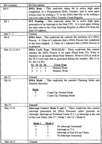
3.1.3.3.
DMA Command/Status Register
This 32-bit
wide
Read/Write
register
provides
Status information
from,
and
Command
information
to,
the
on-board
DMA Controller.
Table
3.1.3.3
on
the
following
page
provides
a
description
of each
of
the
valid
bits
in
the
DMA Control/Status Register.
The DMA
Command
Register
is
either
programmed
explicitly
by
the
Table 3.1.3.3
DMA Command/Status Register Bit Definition:
Bit
Location
Bit
Description
BitO
DMA
Done
-This
read-only
statusbit
is
activehigh
uponcompletion of
a
Programmed DMA
Transfer,
andis
reset upon systemreset;
by
writing
a
"0"
to
the DMA
Start
Bit,
orby
writing
anon-zero value
to the DMA Transfer
Count
Register.
Bitl
INT
Pending
-This
read-only
statusbit
is
activehigh
upongenerationofan
Interrupt
to the
Host CPU. It
is
reset uponwriting
any
data
valueto the
Clear
Interrupt Register
at offset6Ch
from
the
Base
I/O
address.Bits 7
-2
Unused
Bit 8
DMA
Start
-This
read/writebit
controlsthe initiation
ofa
DMA
Process.
A
Value
of0
indicates
that
aDMA
Process has
completedor
has
been
stopped.A
Value
of1 indicates that
aDMA
Process
is
in
progress.Bits
12,11,10,9
DMA
Cycle
Type
S0,S1,S2,S3
-These
read/writebits
control whetherthe DMA Process
is
aninput
(Read from
I/O,
Write
to
Memory)
or an output(Read
from
Memory,
Write
to
I/O)
as
wellasthe
PCI
Cycle
type that
is
generatedduring
the transfer:
(Bit 12
is
S3,
Bit 9
is SO).
S3
S2 SI
SO
CvcleTvne
0
110
Memory
Read
0
111
Memory
Write
Bit 13
Unused
Bit 14
DMA
Mode
-This
read/writebit
controlsChaining
Mode
andMemory
direction.
Mode
0
Count
Up,
Normal Mode
1
Count
Up,
Chaining
Mode
Bit 15
Unused
Bits 17,16
Interrupt Control Mode 0
and
1
These
read/writebits
controlinterrupt
generationfor
DMA
Processes
either generate nointerrupt,
Interrupt
onTerminal
Count
(T.C.)
orInterrupt
atthe
end ofthe
Last
Chain.
(Bit 17
=Mode
1,
Bit 16
=Mode
0)
Mode 1
Mode 0
0
0
No Interrupt
Generated
0
1
Interrupt
onT.C.
1
0
Interrupt
atEnd
ofLast
Chain
1
1
No Interrupt Generated
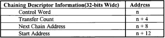
3. 1. 3. 4.
DMA Next Chain Address Pointer Register
This 32-bit
wide
Read/Write
register
specifies
the
address
of
the
next
Chain
Descriptor
to
be
accessed
when
the
DMA Controller
is
in
Chaining
Mode.
This
register
provides
the
link
between
descriptors
during
scatter
or
gather
type
operations.
When
the
DMA Controller
is
initially
programmed
in
Chaining
Mode
this
register
is
programmed
with
the
value of
the
location
of
the
first
Chain in
the
programming
link.
Subsequent
Chaining
information
is
loaded
without programmer
intervention
by
the
DMA Controller
[image:21.586.185.474.270.337.2]once
the
current chain
has been
completed.
A
value of
OOOOOOOOh
indicates
the
final Chain in
the
series.
The format for
a
Chain
Descriptor
in
Memory
is
shown
below.
Table 3.1.3.4
Chain
Descriptor Format:
Chaining
Descriptor Information(32-bits
Wide)
Address
Control Word
nTransfer
Count
n+
4
Next
Chain Address
n +8
Start
Address
n+12The memory locations for
a single
Descriptor
must
reside
in
four
32-bit
aligned
32-bit
wide
contiguous
memory
locations.
Individual
Descriptors may be located
anywhere
within
the
4
Gigabyte System
Memory
Space
as
long
as
they
are
32-bit
aligned.
The 32-bit
Next
Chain Address
values represent
actual physical
memory locations
within
the
System
Memory
Space.
3.1.4.
On-board Data Flow Control
The
on-board
DMA Controller
operates
in
a
Demand Mode
fashion.
When
properly
programmed,
DMA
Operation
commences
upon
the
receipt of a
DMA Request
signal
from
the
Parallel
Interface Control
logic.
This DMA
Request
is based
upon
a
transfer
being initiated,
and
data (or
space
depending
upon
direction
of
transfer)
being
available
in
the
on-board
FIFO
Memory
Buffer.
There
are
two
types
of
DMA
requests
that
may
be
generated
by
the
I/O Interface Logic.
During
normal operation a
Burst
Request
is
performed
by
the
Parallel
Interface Control Logic.
This
causes
the
DMA
Controller
to
attempt
to
perform
data
transfers
until
all
programmed
DMA
transactions
have been
completed.
As
long
as
there
is
a
transfer
request
from
the
DMA Controller
to the
PCI Bus
Interface
Logic,
the
PCI
Bus interface
logic
will
request
the
PCI
bus according
to the
rules
described
in
the
PCI Specification.
Once
a
PCI
transaction
has been
a)
The GNT#
signal on
the
PCI Bus
has been
removed
by
the
PC
Host's PCI Arbiter
and
the
local
on-board
latency
timer
has
expired.
b)
The STOP#
signal
has been
asserted
by
the
slave
device
being
accessed on
the
PCI Bus
indicating
that
it's
transfer
buffer's
are
full in input
mode,
or
empty in
output
mode.
The
PCI Interface
logic
will
remove
it's bus
request signal
(BREQ#)
and
re-initiate
the
arbitration
process
by
re-asserting
BREQ#
upon
the
occurrence of one of
these two
events.
In Input
Mode,
when
PAGE_SYNC
is
active
and
the
FIFO
status
is
"Almost
Full",
DMA Burst
requests
occur.
The
same
is
true
in Output
Mode
when
the
FIFO
status
is
"Almost
Empty"During
Input
Mode,
once
PAGE_SYNC
is
removed
by
the
external
Input
logic,
the
DMA
requests
will
be
non-burst.
This
causes
the
PCI
Transfers
to
contain
a single
data
phase
until
the
FIFO
Memory
Buffer
has
been completely
emptied.
During
this
non-burst
mode
there
will
be
a
single
data
phase
for
each
PCI
Transaction.
This
logic is
in
place
to
prevent
an
overrun
or
underrun
condition
from
occurring
in
the
FIFO's.
3.1.5.
PCI Configuration Region
The PCI Configuration Region
is implemented
via
an
Altera
EPX780
FPGA Device.
A 256
byte
register space organized as
sixty-four
32-bit
words
is implemented
to
perform
the
configuration
functionality.
The PCI
Configuration Region
is
required
in
all
PCI
compliant
devices.
The
register
set
associated
with
this
region
is
configured
at
system
initialization for
proper operation
in
the
host
system.
Since
this
region
is
standard
PCI
fare
it
will
not
be discussed in detail
during
this
thesis,
and
is
considered
beyond
the
scope of
this
investigation.
3.1.6.
Parallel Data Interface
The Parallel Data Interface
is
an
8-bit
Data,
Control,
and
Status
interface
for
communication
between
the
on-board
FIFO memory
buffer
and
the
off-board
I/O
Device.
This
is
a
general
purpose
interface
used
for
demonstration
purposes only.
In
an actual application
this
logic,
which
is
contained
in
a
CPLD,
would
be designed
to
communicate
with
a specific
device
or
set
of
devices.
The
on-board
control
registers
are
used
to
program
the
interface
in
either
the
input
or output mode.
In
input
mode
data is
transferred
from
an
input device
to the
FIFO
based
upon
the
status
of
Input
device
and
the
FIFO
(i.e.
Does
the
input
device have
data
to
send,
the
output mode
data is
transferred
from
the
FIFO
to
an
output
device.
Again,
the
status signals are
used
to
condition
this
transfer.
In
the
CPLD
Source
file
provided
with
this thesis there
are
fourteen
pins
available
for
implementing
a custom
bi-directional interface.
This
flexibility
enables
the
designer
to
connect
the
PCI I/O
board
to
a wide
range
of
devices
without
any
modification
to
the
PCI
interface
logic.
3.1.7.
JTAG Interface
A JTAG
(Joint
Test
Action
Group,
IEEE 1
149.1)
interface is
implemented
in
order
to
enable on-board
programming
of
the
SRAM Logic Array's
in
the
Altera Flexlogic
devices
during
system
debug.
A
standard
20-pin
Insulation Displacement Connector
(IDC)
header is
used
to
interface
the
PCI I/O Board
to
a
PC
parallel
port
based
JTAG programming interface
for
the
Flexlogic.
3.2.
Software
Specification
3.2.1.
Compatibility
The
software
developed
for
this thesis
executes
in
a
DOS 5.0
or greater
environment.
Protected
mode
drivers
are utilized
in
order
to
read
and
write
memory
above
the
1
Megabyte DOS
boundary
in
order
to test
operation of
the
DMA
process.
The
software
is
not
intended
to
be
a robust
end-user
application,
but
rather,
to
demonstrate
the
functionality
and
performance
of
the
PCI DMA
subsystem.
3.2.2.
PCI Plug'n
Play
Usage
The PCI
I/O Board
is
fully
PCI
compliant and supports
the
entire required
Configuration Region.
Because
of
this,
the
diagnostic
software
is
able
to
determine
where
the
board
is located
within
the
system's
I/O
Map
and
perform accesses
to
it
accordingly.
Unlike ISA
or
EISA
type
add-in cards
PCI Boards
require
no
I/O
location. Memory
location,
or
interrupt
jumpers.
3.2.3.
DMA Controller
Programming
3.
2. 3. 1.
Programming
the
DMA
C
in Normal Mode
When
initializing
the
DMA Controller
for
Normal
(non-chaining)
Mode
the
first
programming
operation
is
to
write
bit
8
of
the
DMA
Control Register (DMA
Start)
with
a
"0"
This
ensures
that the
Finally
the
DMA
Controller
should
be
written with
the
appropriate
values
for
the
desired
mode,
as
described in
Table
3.1.3.3,
with
the
DMA
Start
Bit
set
to
a
"1
"
to
initiate
the
DMA Process.
Writing
a
"1"to the
Start Bit
of
the
DMA Controller
causes
the
DMA Controller
to
initiate
a
DMA Transfer
by
requesting
the
PCI
Bus. Once
the
bus has
been
granted
the
DMA Controller
will
drive
the
current address onto
the
PCI Bus along
with
the
appropriate
PCI
Command
signals
to
indicate
the type
of
transfer
as specified
in
Table 3.1.3.3.
Once initiated
the
Normal
Mode DMA Process
will
continue
until
one of
the
following
occurs:
The Transfer Count Register
has
reached a value of zero.
The DMA Start
bit in
the
DMA Control Register
is
written
with
a
Zero (Process
will
be
suspended
at
the
completion
of
the
current
transaction,
and
may
be
restarted
by
rewriting
the
DMA
Start
bit
with
a
One).
3.2.3.2.
Programming
the
DMAC
in
Chaining
Mode
When
initializing
the
DMA Controller
for
Chaining
Mode,
the
first
programming
operation
is
to
write
bit
8
of
the
DMA Control
Register
(DMA
Start)
with
a
"0"This
ensures
that the
DMA
Controller
is
in
a
halted
state.
Prior
to
initiating
the
DMA Process
by
programming
the
DMA
Control
Register
for
the
desired
chaining
operation,
the
Chaining
Descriptors
should
be
programmed
in System Memory. Each chaining
descriptor
must
be
located
at
a
32-bit
aligned
address.
This
enables
the
DMA
Controller
to
properly fetch
the
chaining
information.
The chaining
descriptors do
not
need
to
be located in
a
contiguous
block
of
memory.
Each
descriptor
may
exist anywhere
in memory
as
long
as
the
address
is
32-bit
aligned.
The Next
Chain
Address Pointer
Register
within
the
DMAC
should
be
programmed
after
the
chaining
descriptors have been loaded into
system memory.
The
value
of
this
register should
be
the
base
address of
the
first chaining
descriptor
in System
Memory.
The
Source Address
and
Transfer
Count
Registers
are
don't
care
values
for
the
Chaining
Mode
initialization
process.
They
will
be loaded
by
the
DMA
controller
when
the
first chaining descriptor is
accessed.
Programming
the
Next
Address
Pointer Register
enables
the
DMA
Controller
to
operate
in
Chaining
Mode according
to the
description
in
Table
3.1.3.3,
and
the
DMA Start
bit
may
be
set
to
a
"1"to
initiate
the
DMA Process.
Once
initiated,
the
Chaining
Mode Process
will
continue
until
the
Transfer Count
has
reached zero and
the
Next
Address Pointer
has
been loaded
with
null
descriptor
reference
(OOOOOOOOh).
As
presented
in
the
Control Register Bit
Definition,
an
interrupt
may
be
generated at
the
end of
each
chain
(each
time
Terminal
Count
Reaches
Zero),
at
the
end of
the
last
chain
(Terminal Count
is
Zero
and
Next
Address
Pointer
is
Zero),
or not
at
all.
This may
be
changed
on
a chain
by
chain
basis
as
the
Control Word
is
the
first
value
loaded
during
the
chaining
process.
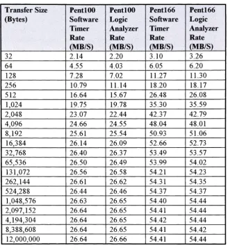
4.
Analysis
Performance
data
acquired
during
testing
is
presented and analyzed.
Two
measurement
techniques
were
invoked in
order
ensure
the
data
obtain was
accurate.
Two
popular
PCI
systems were
used
to
host
the
PCI I/O
board for
these
performance measurements.
4.1.
Performance Measurement
One
of
the
main
goals
during
the
development
of
this thesis
was
data
movement
performance.
This
system architecture was
defined
to
enable
the
DMA Controller
to
operate
with rninimal
CPU
overhead.
This
accomplishes
two
goals:
1)
The
CPU is
freed
up
to
perform other
tasks
2)
The
overall
DMA
task
becomes
more efficient
Data
throughput
was
performed
in
two
different
types
of
Personal Computer
Systems.
This
was
done
to
demonstrate
that
overall
performance
is
greatly
dependent
upon
the
performance of
the
PCI
system
in
which
the
PCI I/O
board
resides.
Additionally,
two
independent
measurement
techni