Recent advancements towards Green Optical Networks
Alan Davidson*
a, Ivan Glesk
a, Adrianus Buis
b, Junjia Wang
c, Lawrence Chen
ca
Dept. of Electronic and Electrical Engineering, Faculty of Engineering, University of Strathclyde,
204 George Street, Glasgow, G1 1XW, United Kingdom
; bDept. of Biomedical Engineering, Faculty
of Engineering, University of Strathclyde, 106 Rottenrow, Glasgow, G1 1XW, United Kingdom;
cDepartment of Electrical and Computer Engineering, McGill University, 480 University Street,
Montreal, H3A 0E9
ABSTRACT
Recent years have seen a rapid growth in demand for ultra high speed data transmission with end users expecting fast, high bandwidth network access. With this rapid growth in demand, data centres are under pressure to provide ever increasing data rates through their networks and at the same time improve the quality of data handling in terms of reduced latency, increased scalability and improved channel speed for users. However as data rates increase, present technology based on well-established CMOS technology is becoming increasingly difficult to scale and consequently data networks are struggling to satisfy current network demand. In this paper the interrelated issues of electronic scalability, power consumption, limited copper interconnect bandwidth and the limited speed of CMOS electronics will be explored alongside the tremendous bandwidth potential of optical fibre based photonic networks. Some applications of photonics to help alleviate the speed and latency in data networks will be discussed.
Keywords: Electronic Bottleneck, Optical Interconnect, Data centre Network, Scalability, Optical Switching
INTRODUCTION
based processing cannot continue to scale to sustain the ever increasing serial data rates that WDM backbones and metro networks will deliver and as a result, electronic bottlenecks will result.
THE ELECTRONIC BOTTLENECK
CMOS scaling limitations
The well-known CMOS transistor scaling rules first described by Robert Dennard in 1974 describes how transistor size can be reduced while at the same time increasing switching speed and reducing power consumption5. Dennard scaling states that as transistor size reduces, power consumption will reduce while maximum clock speed can be increased. An important observation of Dennard scaling is that power density (Watts/unit chip area) has remained approximately constant as transistor density has increased. In addition, the density of transistors has been increasing by a factor of about two every 18 months for over 40 years. Gordon Moore first suggested such an exponential improvement in transistor density back in 1965 with an estimated doubling of transistor density every two years6. What has actually happened since then has validated what became known as ‘Moore’s law’ despite the increasing technical challenges of integration. This trend is forecast by Intel to continue until around 20207.
However, despite the continuing validity of Moore’s law, Dennard scaling came to an end in 2005 with the development of 90nm lithography. At this level, transistor gates become too thin to prevent current from leaking into the substrate. In addition, threshold voltage scaling has resulted in an increase in junction leakage currents. Pd = CV2F expresses the
relationship between clock frequency F and the transistor dynamic switching power consumption Pd; where C is the
CMOS switch lumped capacitance which is the sum of the junction and gate capacitances; and 𝑉 is the supply voltage8.
In 2005, leakage current became a problem at the 90nm node. Previously, transistor dimensions reduced, C reduced allowing F to be increased and V to be reduced (since the threshold voltage scales with the gate oxide layer thickness) while at the same time reducing the power consumption Pd and maintaining the overall power density of the chip
constant. Performance per watt rose as transistor density increased and therefore the energy per bit reduced. However, leakage current has become an issue due to the scaling of the gate oxide thickness which increases gate oxide tunneling and the scaling of the threshold voltage which increases sub-threshold currents. These leakage currents have resulted in a rise in chip static power density, and in the case of junction leakage currents present the possibility of spontaneous transistor state switching leading to errors and corruption of data if allowed to get too high. The supply voltage (V) scaling ended at around 1V and helped mitigate the rise in junction leakage current by increasing the threshold voltage, however this has been at the expense of the dynamic power consumption which is proportional to V2 and chip power density Pd has therefore been increasing as a result. The clock frequency F is therefore limited to avoid excessive total
power density. High power density runs the risk of causing thermal runaway and destruction of the chip in addition to creating cooling challenges and power consumption cost issues when scaled to the size of a data center. In the short term it is clear that increasing clock speeds to satisfy demand is therefore not a realistic option.
Electronic Interconnect scaling limitations
As data centers scale to meet demand, rack and switching/routing copper interconnects must get longer to connect server racks to each other and to routers and switches. The number and total length of interconnects will therefore increase exponentially with scaling. As a consequence, increasing power consumption will result since the capacitance of each interconnect rises with the length of interconnect; and the bandwidth of the copper interconnects will reduce as the delay increases as a result of increasing resistance and capacitance. Thus copper interconnects and electronic switches in data centres are limited to 10Gb/s serial data rates per channel with a maximum range in the 10’s metres with 100m possible at very high power consumption. To circumvent this problem, data centers have widely employed optical fiber interconnects. While these have solved the issues of space and reach, they use CMOS based optical/electronic/optical (OEO) transceivers which until recently have been limited to 10Gb/s. However, Intel have announced a new MXC type optical interconnect which is designed to connect top of the rack (ToR) switches to each other and to the core switches or to connect servers to extra storage or graphic processing units (GPU’s). This interconnect is capable of 800Gb/s in total each way with a maximum of 25Gb/s serial data rate per fiber (64 fibers with 32 each way)10. It can operate up to 300m at reduced power consumption compared with copper cables. While this technology can overcome the attenuation and bandwidth limits of copper cables, it still requires bandwidth-limited and power hungry OEO transceivers.
Computing speed limitations
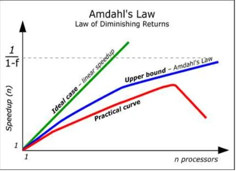
[image:3.595.180.417.475.647.2]While parallelism can do nothing to reduce power consumption or help overcome interconnect bandwidth limitations, it can contribute to reducing latency by speeding up the processing of requests. We have shown, leakage current and global interconnect problems have made it necessary to limit power consumption by reducing the clock frequency and therefore also the processing speed. Consequently, since 2005 chip manufacturers Intel and AMD have concentrated on introducing parallel processing CPUs using multicore processors to increase processing power with the latest high performance server processors capable of supporting 10Gb/s data rates. While parallel processing can, to a degree compensate for limited clock frequencies by providing a speed-up in computing, it clearly results in power consumption since an effective doubling in performance requires at least two processors. In addition, Amdahl’s parallelism law states that ‘If a computation has a serial component f% and a parallel component p%, then the maximum speed-up given an infinite number of processors is (f+p)/f. Clearly, the greater the parallel portion p, the higher the speed-up11. However there is a fundamental maximum improvement in computational speed that is dependent upon the proportion of serial computation, beyond which further additional parallel processors will contribute a rapidly diminishing improvement in processing speed. Consequently the performance per watt which is initially constant will eventually decrease rapidly as the number of processors is increased beyond the optimum number. This principle is illustrated in Figure. 1. As the number of parallel processors n increases the maximum speed-up value is achieved, beyond which adding more processors provides diminishing additional computational advantage and increases power consumption.
In fact, when a request is implemented in a parallel computing system, the overall response time is dictated by the distribution of parallel operations and therefore by the slowest operation. Therefore every operation must have a low latency. In the longer term, the answer to satisfying the rapid increase in demand for processing power in data centers will therefore not be found using present CMOS electronic technology. The fundamental limits of electronic data switching may be reached sooner rather than later. In the short term, while Moore’s law holds and effective cooling can be achieved, processing speeds will continue to rise. However power density is no longer constant as previously predicted by Dennard’s Law but will increase with processor density. The fundamental limits to parallelism indicated by Amdahl’s law and limits to the sustainable power density in CMOS based processors dictated by thermal runaway and processor/cooling power consumption lead to a fundamental limit on the processing power of present electronic data centers.
Research into reducing CMOS leakage currents has demonstrated improvements in data handling capacity and power efficiency12. However, these improvements have been slow with only modest gains in reduced leakage current achieved. Graphene13 and nanowire14 technologies are being investigated as a replacement for current CMOS based devices. However, research in these areas is in its infancy and operational devices are many years frommarket. Many groups are currently working on a photonic alternatives for the electronic transistor and a few of these technologies are discussed in section 5.
OPTICAL NETWORKS AND DATA CENTERS
Bandwidth of optical fiber
The very high bandwidth of optical fiber and the rapid increase in demand for data transmission bandwidth have resulted in fiber optics technology becoming an important building block in data networks. In fact optical fiber has become one of the fastest growing transmission media for new data network installations and upgrades15; and has become ubiquitous in long haul communications and present transmission rates exceed 1Tb/s over long distances on a single fiber. In a similar way, the use of optical fiber for interconnects and all-optical switching within the data center opens up the possibility of alleviating the electronic bottleneck by greatly improved bandwidth, lower power consumption and lower attenuation than copper based interconnects. In addition to high bandwidth, optical fiber has several significant advantages over traditional copper cabling including:
Low attenuation allowing much longer distances between repeaters.
No resistive heating.
Immunity to electromagnetic interference, crosstalk and corrosion.
More durable, compact and lighter in weight.
Higher CAPEX but lower overall cost in the long term.
To take full advantage of the low attenuation of around 0.15 to 0.2 dB/km in the 3rd window C-band frequency range (1525nm–1565nm) and the development of the Erbium Doped Fiber Amplifier (EDFA), Dense Wavelength Division Multiplexing (DWDM) was developed. Today, modern transmission systems can easily transmit 160 wavelength data channels at 10 Gb/s each over a single fiber, creating aggregate throughput of 1.6 Tb/s. Despite the low attenuation and without the availability of optical amplifiers signal regeneration was required particularly in long haul fiber optic systems. Around 1990, the EDFA (Raman Amplifiers16) became available allowing optical signal amplification without the need for OEO conversion.
In today’s networks the use of state of the art optical technologies has vastly improved single wavelength channel data rates. Serial data rates per a single optical wavelength channel have grown from the adoption of OC-1 in 1980 to a maximum of OC-678 equivalent to 40Gb/s possible today. OC-n refers to the serial data capacity 𝑛 ∗ 51.84 Mb/s of each optical carrier in a dense wave division multiplex (DWDM) configuration.
systems are commercially available which use OC-678 across 80 channels with a 50GHz ITU grid. The bandwidth used is therefore 4THz and the total bit rate achieved is 80 ∗ 678 ∗ 51.48 Mb/s or approximately 1.4Tb/s.
The following analysis illustrates the theoretically immense capacity of optical fiber. The theoretical maximum capacity at the maximum sampling rate (or symbol rate) of a band-limited noise free channel is given by the well- known Nyquist theorem:
C = 2Blog2(2n)
Where C is the channel capacity in bits per second (b/s); B is the bandwidth (in this case of the fiber) in Hertz (Hz); and n is the number of bits used to describe each symbol. This theorem states that the maximum symbol transmission rate is twice the bandwidth of the channel to avoid inter-symbol interference (ISI) with neighboring samples. Apparently the channel can carry an infinite amount of information by simply increasing n, however a noise free channel is unattainable. Using the well-known Shannon-Hartley theorem, the theoretical maximum capacity in the presence of noise is given by:
C = Blog2(1+ (𝔓/Bhγo) 1/2
)
Where C and B are as before, 𝔓 is the power guided by the fiber in Watts, h is Planck’s constant; and 𝛾0 is the centre frequency of the fibre bandwidth in Hz. The quantity (𝔓/Bhγo)1/2 is the signal to noise ratio of the channel measured as
the ratio of the average received signal power to channel quantum shot noise at the receiver. It is assumed that the potential bandwidth of fiber is of the order of 50THz. In the use of this figure it is assumed that there is a sharp roll-off which is limited by the attenuation in the fiber medium increasing outside its transmission window. The center frequency 𝛾0 is taken to be that corresponding to the minimum attenuation of fibre at a wavelength of 1550nm. As a rule of thumb the maximum value of 𝔓 is around 100W. This limitation is due mainly to heating in the fiber around imperfections which will result in the eventual catastrophic destruction of the fiber at power input levels above the rate at which the fiber can dissipate heat. High powers will also cause dispersion through nonlinear refractive index dependence on the input power resulting in a reduction in capacity. In addition, stimulated Brillouin and Raman scattering will result in an increase in noise proportional to 𝔓 which will quickly outweigh the quantum shot noise and therefore result in a reduction in maximum channel capacity. Substitution of these values into the above equations results in an ideal theoretical maximum value of C at about a colossal 600Tb/s for a single mode fiber. It’s worth noting that the capacity of a very long fiber will be reduced due to attenuation. The present experimental limit is around 100Tb/s using multi-core fiber over many 10’s of kilometers17
. It is therefore clear that optical fiber has the potential to meet future demand for very high serial data rates; and given the necessary serial WDM channel MUX/DEMUX and optical switching technology, optical fiber could be utilized to provide highly scalable, high speed all-optical interconnects in data networks.
Despite the many technical challenges to the realization of all-optical data networks, advances have been made in the use of optical routing in data networks. The recent development of the reconfigurable optical add/drop multiplexer (ROADM) has allowed the reduction in use of power hungry and band limited OEO transceivers in optical cross connects for data network metro and long haul nodes18. ROADMs allow individual DWDM wavelengths to be added or dropped. However wavelength granularity is low and the best systems use 80 channel wavelengths. Electronic time division MUX/DEMUX for example allows the capacity of each channel to be better utilized. However, electronic switching speed limits full use of the channel bandwidth available. For example, using a 50GHz ITU grid, the theoretical capacity of each channel is around 0.5Tb/s per wavelength channel based on the capacity calculation in section above. The best OC-768 systems presently manage only 768*51.84Mb/s or around 40Gb/s due to bandwidth limited electronic switching.
Intra data center schemes
and highly scalable, high port count all-optical switches; and promise reduced contention, latency and power consumption.
Helios19 is a hybrid 2-layer WDM based architecture using modular performance optimized data center (POD) units. At the POD layer, packet switching is achieved using conventional electronic commodity switches; and at the core layer, optical circuit switching is used in parallel with commodity packet switching. Optical circuit switching is achieved using MEMS switches in WDM links, facilitating the use of optical interconnects and reducing the requirement for power hungry transceivers and commodity switches. This scheme is ideally suited to long-term transfers between racks, however, using MEMS switches it suffers from high reconfiguration times of around 15ms. However, ultimately both systems are limited by the need for electronic packet switching since the optical buffering required for all-optical packet switching (OPS) has not yet been realized.
Mordia20 is a hybrid network that uses wavelength selective switches (WSS) for optical circuit switching in WDM links. Each node contains a WSS and Ethernet 10G commodity packet switches. Wavelengths can be added or dropped at each node using the OCS. The main advantage of this system over Helios is a faster optical circuit reconfiguration time of 11.5μs.
A recent approach to achieving a form of optical packet switching is the DOS (Datacenter Optical Switch) architecture21. Here the switching of optical packets is based on an arrayed waveguide grating router (AWGR) switching fabric where different inputs can reach the same output simultaneously using different wavelengths avoiding contention in the wavelength domain. This non-blocking switching is achieved using a tunable wavelength converter at each node. By selectively tuning the wavelength converter, a node can access any other node via the AWGR and packets are therefore routed accordingly. This system is power efficient too since the signal is delivered to the output port via a specific wavelength rather than using broadcast and select where associated power dividing losses occur. In simulations low latency, high-throughput switching was reported. In addition, latency was found to be almost independent of the number of input ports and saturation did not occur even at 90% input loads. The AWGR with tunable wavelength converter switch uses mechanisms such as the third order non-linearity four-wave mixing (FWM) and cross-phase modulation (XPM) in addition to second order non-linear effects to achieve wavelength conversion. Tuning is achieved by changing the wavelength of the pump laser. The non-linear processes outlined above produce an output from the wavelength conversion medium at a different wavelength to the input signal wavelength. The AWGR will therefore route the wavelength shifted signal to a different port. Fast tuneable lasers and non-linear media are required to ensure switching rates suitable for packet switching. Successful tuning of an input signal with wavelength 1546nm to generate an output signal over the range 1535 to 1557nm at 40Gb/s has been achieved22.
III-NITRIDE PHOTONICS FOR DATA CENTERS
reducing power consumption. Despite attempts to artificially induce a 2nd order non-linear characteristic by, for example introducing strain to the crystal. However the field of strained silicon photonics is still in its infancy.
Recently, III-nitride semiconductors have been identified as contenders for the development of high speed inter sub-band (ISB) devices for application in data networks and in other areas. III-nitride semiconductors that show promise are Gallium Nitride (GaN) and Aluminium Gallium Nitride (AlGaN) and their alloy. These III-nitride wide bandgap semiconductor materials are compatible with CMOS fabrication techniques and they exhibit the 2nd order non-linearity required for lasing and high speed electro-optic devices for modulation and switching in data networks. Such devices would reduce the need for OEO transceivers and electronic switching and reduce power consumption.
III-nitride materials may therefore hold the answer to reducing interconnect power consumption and allow single channel serial data rates (which maxed out at 40Gb/s (OC -768) around 2007) to be exceeded. With a large conduction band offset of about 1.8 eV and a sub-picosecond ISB relaxation time, these materials are therefore attractive for the development of the ultrafast photonic devices in the near infra-red ideal for use in data networks. In addition, these materials can operate at high temperatures, high power and they exhibit low attenuation in the near infrared wavelength region because of their wide band-gap. Modulation of III-nitride refractive indexes is possible by carrier injection making these materials compatible for use as modulators in fibre optic based communication systems. These features make III-nitride materials attractive for the development of tuneable optical phased array devices not possible with silicon such as AWGRs used in data networks for WDM MUX and DEMUX. Devices that have been realised in the lab include 2x2 directional couplers and an eight wavelength AWGR.
Quantum Cascade Photodetectors
Unlike quantum well infrared photodetectors (QWIPs), quantum cascade detectors (QCDs) are photovoltaic devices that can be operated at zero bias and therefore need no power supply. In both types of devices, detection relies on photon absorption by electronic sub-band transitions in semiconductor quantum wells (QWs) and the operating wavelength can be widely tuned by choice of the QW thickness.
A room temperature QCD employing a GaN/AlGaN/AlN heterostructure has been reported24. The design takes advantage of the large internal field that exists in III-nitride semiconductors to generate the essential saw tooth energy level structure. This device operates in the near-IR spectral range covering the all important optical fiber low attenuation c-band. It was shown to exhibit room temperature responsivity of 10mA /W or 1000V/W at zero bias and at a wavelength of 1700nm. A GaN/AlGaN QCD has been demonstrated25. It was suggested that speeds in excess of 80GHz could be achieved by reducing the mesa size.
Electro-optic Modulators
The realization of an efficient electro-optic modulator requires strong second order susceptibility (χ(2)). A strong χ(2) susceptibility was demonstrated using a device based on the integration of a single crystal of GaN on a Si (100) substrate heterostructure26. This device uses engineered GaN micro-rings to provide dual resonance at wavelengths of 1560nm and 780nm. Efficient tunable second harmonic generation at 780nm was demonstrated and the χ(2) susceptibility was
measured as high as 16±7 pm/V. Since GaN has a wide transparency window, this device structure was suggested to be a viable route for the second harmonic generation of optical wavelengths in the range from far-IR to near-UV enabled by a combination of χ(2) sum and difference frequency processes. It is suggested that the strong χ(2) susceptibilities reported
using GaN on Si platform will be useful in the development of electro-optic modulators and optical parametric oscillators.
An electro-optic modulator based on three periods of 1.3nm thick GaN QWs with 3nm thick AlN barriers grown on a 1µm AlN template has been demonstrated27. The wells were n-doped with Si at 2×1019 cm–3 with the active region sandwiched between two 500 nm thick Al0.5Ga0.5N bottom and top contact layers which were n-doped with Si at
voltage swing of ±5V was recorded. A 12db modulation depth of 12db is required for optical modulators to comply with the 10-12 bit error rate (BER) standard used in fiber optic data networks.
A room temperature electro-optic modulator based on electroabsorption modulation over the wavelength ranges 1200nm to 1670nm and 2100nm to 2400nm in GaN/AlN coupled QWs has been demonstrated28. The electro-modulation reported is due to electron tunneling between a wide well reservoir and a narrow well separated by an ultrathin AlN barrier. The maximum modulation depth reported was 44% at a wavelength of 2200nm. The -3db cut-off was measured at 11.5MHz with a device mesa size of 700μm2 and is limited by the RC time constant. It was suggested that a much
larger cut-off frequency should be attainable with smaller mesa sizes.
Arrayed Waveguide Gratings
nitride materials are better suited for the development of AWG’s than silicon or InP since the refractive index of III-nitrides is less than 2.3 making them more compatible with coupling with silica fibers; and intrinsic losses are lower due to a wide band gap compared to the 1550nm application wavelength. A 1x8 GaN-AlGaN based WDM demultiplexer AWG with one input waveguide and 8 output waveguides has been demonstrated29. The fabrication process involved photolithographic patterning and dry etching. The AWG was designed to give an output spacing of 2nm. The reported rejection ration of 10 was measured for most of the output ports.
All-Optical Switches
The non-linear properties of Silicon doped GaN/AlN quantum dot (QD) and quantum well (QW) superlattices were evaluated for the development of all-optical switches and wavelength converters for data networks operating at room temperature and at a wavelength of 1550nm30. The third order non-linear susceptibility measured was 5 times larger in the QD samples than in the QW samples and this result is attributed to higher quantum confinement. The ultrafast nature (100fs) of ISB transitions in addition to the higher third order susceptibility make GaN/AlN heterostructures good candidates for the development of all-optical high speed, high contrast ratio and low saturation intensity devices suitable for applications in multi terabit data networks.
ISB transitions in GaN QWs for use as an all-optical switch were investigated31. For a -3db extinction, a switching power of 100pJ was reported improving to 25pJ. All-optical switching was verified for wavelengths of 1550nm and 1700nm and the device was able to operate for 4 pulses with an interval of 1ps. An extinction ratio better than 10dB was reported.
TOWARD ALL-OPTICAL SIGNAL PROCESSING
It is clear from the discussion that the fundamental limits on electronic switching speeds and parallel processing will in the near future severely affect the ability of data networks to satisfy, both quantitatively and qualitatively, the exponentially increasing demand for data. While the introduction of all-optical switching schemes32-34 and optical interconnects can improve latency, contention and capacity, a new solution is required to improve processing speed to take full advantage of the potential serial data rate capacity of such systems. The requirement for a new disruptive technology is therefore inevitable. Ideally, development of a photonic transistor allowing faster switching which is compatible with CMOS fabrication techniques would allow cheaper to market solutions than developing an all new ground-up fabrication technology. Silicon photonics devices can be fabricated using present CMOS fabrication techniques and therefore this technology is being investigated for the development of future optical signal processing systems32.
Chen et al have demonstrated an optical transistor where a single stored gate photon can control the transmission of applied source photons35. Since the source requires only one photon to control the source output, the potential exists for extremely low switching power consumption. In addition, since photons are effectively stored, this principle may be applicable to the development of the much sought after optical memory necessary for buffering data in data networks. However, the transistor is clearly not compatible with CMOS fabrication and since it requires three lasers for the gate and source; and lasers to allow super-cooling of the caesium gas, it is unlikely to provide a practical solution in the foreseeable future. The terms ‘gate’ and ‘source’ are used as an analogue to the CMOS FET transistor.
Another approach by Varghese et al is the development of a silicon optical transistor which uses an asymmetric coupled add/drop filter consisting of a micro-ring resonator next to an optical waveguide representing the source36. Normally light will pass through the source waveguide and exit unaffected since weak source coupling with the micro-ring ensures that nonlinear effects are negligible. Its resonance will therefore remain unaffected. However, at a specific resonant frequency the light will interact with the micro-ring resonator greatly reducing the output and changing the state to off. This change in resonant frequency is achieved using another optical waveguide representing the gate. The device is reported to operate at 10GHz. A notable advantage of this technology is compatibility with current state of the art CMOS fabrication techniques allowing scalability and avoiding the need to develop new fabrication techniques from the ground up. However, it is clear that the development of the optical CPU and the all-optical data signal processing is in the very distant future.
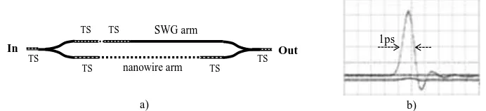
Given a future where networks will need to perform ultra-high speed serial data processing all optically; there will be basic requirements for all optical MUX/DEMUX devices capable of performing at speeds well beyond that available today. To overcome this electronic bottleneck Glesk et al developed an ultrafast all optical photonic switch37-38 which does not suffer from the currier recovery time limitations affecting all optical switches based on SOA32 demonstrated previously. The schematic of this novel device is shown in Fig. 3(a) and its sub picosecond switching capabilities in Fig. 2(b). This novel photonic switch can be used as a self-switched all-optical Timing gate, TG.
Figure. 2(a) Illustration of a self-switching all optical Timing Gate TG; (b) demonstration of its terabit/s switching capabilities. TS –tapered section, SWG –subwavelength waveguide gating
TG has a Mach-Zehnder interferometric structure with one arm composed of a Si nanowire. The second arm is a subwavelength waveguide grating (SWG) structure. Tapered sections marked TS are added to properly balance device properties and the loss to help achieve complete interferometric switching.
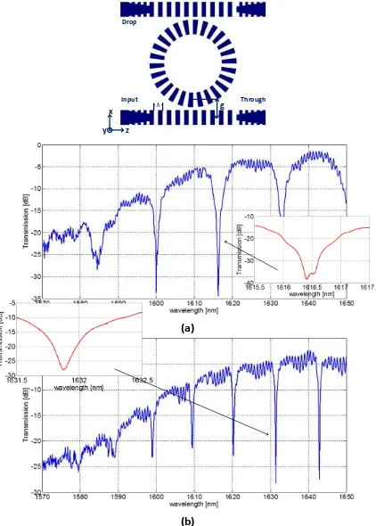
However there is a growing need to develop a library of integrated devices for performing a variety of all optical signal processing functions in application in data centers. One key function needed is a wavelength filtering. By taking advantage of the ability to tailor the effective index of SWG waveguides, Wang et al39 proposed a type of integrated filtering device (which can also provide also an Add/Drop functionality) based on combination of SWG waveguides and ring resonators (Fig. 3). The biggest advantage for these SWG Bragg grating filtering devices is that the peak reflection wavelength can be tuned very easily by adjusting the duty cycle of the SWG.
Out In
SWG arm
nanowire arm
a)
1ps
b)
TS
TS TS
TS TS
[image:9.595.124.470.383.462.2](a)
(b)
[image:10.595.87.509.72.662.2](c)
Figure. 3 All optical integrated Add/Drop device based on SWG waveguide ring resonator: schematic and typical measured responses for ring radii of (a) 10 m, (b) 15 m.
74
z x y
Λ g
Input Through
CONCLUSIONS
Optical fibre networks have a vast potential data handling capacity. However this capability is becoming severely limited by serial data processing speed abilities of currently available CMOS electronics. Speed-up using parallel processing is confounded by the fundamental limits of Amdahl’s Law. This scenario will soon hinder the ability of data networks to scale up to meet exponentially increasing demand for capacity. While all-optical wavelength routing can help improve data network throughput, ultimately at network endpoints any such improvement will be choked by fundamentally limited CMOS electronic signal processing capabilities. There is a need for the development of a disruptive technology to overcome this bottleneck. A promising candidate is all-optical signal processing. Progress has been made in the development of the photonic devices necessary to achieve this goal. However any further progress will require speedy development of ultrafast “all-optical transistor” based photonic logic gates.
ACKNOWLEDGMENTS
This work was supported by the NSERC NGON CREATE program and the Royal Society under the International Exchanges Scheme 2012/R2.
REFERENCES
[1] “Cisco Global Cloud Index: Forecast and Methodology, 2012-2017,” Cisco,
<
http://www.cisco.com/c/en/us/solutions/collateral/service-provider/global-cloud-index.gci/Cloud_Index_White_Paper.html> (30 March 2014).
[2] “Explosive Growth in Data Traffic and the future of Global Communications Infrastructure,” Ntt, <http://www.ntt.com/resource-centre/article/data/global-watch02.html> (30 March 2014).
[3] Barney, D., “The great cloud bottleneck: How capacity issues can kill your cloud project.” Redmondmag, <http://redmondmag.com/articles/2011/12/01/cloud-bottleneck-issues.aspx> (30 March 2014).
[4] Hruska, J., “The death of CPU scaling: From one core to many – and why we’re still stuck,” Extremetech, 1 February 2012, <http//www.extremetech.com/computing/116561-the-death-of-cpu-scaling-from-one-core-to-many-and-why-were-still-stuck> (30 March 2014).
[5] Dennard, R. H. et al., “Design of ion-implanted MOSFETs with very small physical dimensions,” IEEE Journal of Solid-State Circuits, 9(5) (1974).
[6] Moore, G. “Cramming More Components onto Integrated Circuits,” Electron. Mag. 38(8) 20 – 27 (1965). [7] Hruska, J., “Intel’s former chief architect: Moore’s law will be dead within a decade,” Extremetech, 30 August,
2013, <http//www.extremetech.com/computing/165331-intels-chief-architect-moores-law-will-be-dead-within-a-decade> (30 March 2014).
[8] Chandrakasan, A. P., and Brodersen, R. W., "Minimizing power consumption in digital CMOS circuits," Proceedings IEEE 83(4), 498-523 (1995).
[9] Havemann, R.H.; Hutchby, J.A, "High-performance interconnects: an integration overview," Proceedings IEEE 89(5), 586-601 (2001).
[10] Brodkin, J., ‘‘Intel’s 800 Gbps cables headed to cloud data centers and supercomputers,’’ Arstechnica, 10 March 2014, <http//www.arstechnica.com/information-technology/2014/03/intels-800gbps-cables-headed-to-cloud-data-centers-and-supercomputers/> (22 September 2014).
[11] Brian, T., ‘‘Putting multicore processing in context: Part One,’’ Embedded, 9 January 2006, < http://ww.embedded.com/design/mcus-processors-and-socs/4006507/Putting-multicore-processing-in-context-Part-One> (22 September 2014).
[12] Singh, S. K., Kaushik, B. K., Chauhan, D. S., and Kum, S., “Reduction of Subthreshold Leakage Current in MOS Transistors,” World Applied Sciences Journal 25(3) 446-450 (2013).
[13] Graham-Rowe, D., “Better Graphene Transistors,” Technologyreview, 17 March 2008, <http://www.technologyreview.com/news/409775/better-graphine-transistors/> (30 March 2014).
[14] “New ‘4-D’ Transistor is preview of future computers,” Purdue, 4 December 2012, <
Error! Hyperlink
[15] ‘‘The Optical Fibre Advantage,’’ Syringanetworks,
<http://www.syringanetworks.net/resources/industry_library/the_optical_fiber_advantage/> (22 Sept 2014). [16] Singh, S. and Kaler, R.S., "Flat-Gain L-Band Raman-EDFA Hybrid Optical Amplifier for Dense Wavelength
Division Multiplexed System," IEEE Photonics Technology Letters, 25(3) 250-252 (2013).
[17] Sakaguchi, J., Awaji, Y., Wada, N., Kanno, A., Kawanishi, T., Hayashi, T., Taru, T., Kobayashi, T., and Watanabe, M., "Space Division Multiplexed Transmission of 109-Tb/s Data Signals Using Homogeneous Seven-Core Fiber," Journal of Lightwave Technology 30(4), 658-665 (2012).
[18] “Advances in Roadm Technologies and Subsystems,” Enablence, <
Error! Hyperlink reference not
valid.
> (22 September 2014).[19] Farrington, N., ‘’Helios: a hybrid electrical/optical switch architecture for modular data centres.’’ ACM SIGCOMM Computer Communication Review 41(4), 39-350 (2011).
[20] Porter, G., "Integrating microsecond circuit switching into the data center," Proceedings of the ACM SIGCOMM 2013 conference on SIGCOMM. ACM, 2013.
[21] Xiaohui Y., Yawei, Y., Yoo, S. J. B., Mejia, P., Proietti, R., and Akella, V., "DOS - A scalable optical switch for datacenters," Architectures for Networking and Communications Systems (ANCS), 2010 ACM/IEEE Symposium on 7(2) 1-12 (2010).
[22] Hu, H., "Tunable all-optical wavelength conversion based on cascaded SHG/DFG in a Ti: PPLN waveguide using a single CW control laser." IEEE Photonics Journal4(5), 1396-1400 (2012).
[23] Solomon, A.,"A 90nm CMOS integrated nano-photonics technology for 25Gbps WDM optical communications applications," Electron Devices Meeting (IEDM) (2012).
[24] Vardi, A., "Near infrared quantum cascade detector in GaN∕ AlGaN∕ AlN heterostructures," Applied Physics Letters 92(1) 011112 (2008).
[25] Vardi, A., "High-speed operation of GaN/AlGaN quantum cascade detectors at λ = 1.55 μm." Applied Physics Letters 93(19), 193509-193509 (2008).
[26] Xiong, Ch., "Integrated GaN photonic circuits on silicon (100) for second harmonic generation," Optics express 19(11), 10462-10470 (2011).
[27] Machhadani, H., et al. "GaN/AlGaN intersubband optoelectronic devices," New Journal of Physics 11(12), 125023 (2009).
[28] Nevou, L., "Short-wavelength intersubband electroabsorption modulation based on electron tunneling between GaN/AlN coupled quantum wells," Applied physics letters 90(22) 223511-223511 (2007).
[29] Hui, R., "III-nitride-based planar lightwave circuits for long wavelength optical communications," IEEE Journal of Quantum Electronics 41(1), 100-110 (2005).
[30] Guillot, F., "Si-doped GaN∕ AlN quantum dot superlattices for optoelectronics at telecommunication wavelengths," Journal of applied physics 100(4) 044326 (2006).
[31] Norio, I., Kaneko, K., and Suzuki N., "All-optical switch utilizing intersubband transition in GaN quantum wells," IEEE Journal of Quantum Electronics 42(8), 765-771 (2006).
[32] Sokoloff, J. P., Prucnal, P. R., Glesk, I., Kane, M., "A terahertz optical asymmetric demultiplexer (TOAD)," IEEE Photonics Technology Letters 5(7) 787-790 (1993).
[33] Glesk, I., Sokoloff, J. P., and Prucnal, P. R., "Demonstration of all-optical demultiplexing of TDM Data at 250 Gb/s," Electronics Letters 30(4), 339-341 (1994).
[34] Glesk, I., Prucnal, P.R., and Andonovic, I., “Incoherent ultrafast OCDMA receiver design with 2 ps all-optical time gate to suppress multiple-access interference,” IEEE J. Sel. Top. Quantum Electron. 14, 861-867 (2008). [35] Chen, W., Beck, K. M., Bücker, R., Gullans, M., Lukin, M. D., Tanji-Suzuki, H., and Vuletić, V., "All-Optical
Switch and Transistor Gated by One Stored Photon," Science341(6147) 68-770 (2013).
[36] Varghese, L., Fan, L., Wang, J., Gan, F., Wang, X., Wirth, J., Niu, B., Tansarawiput, C., Xuan, Y., Weiner, A. Qi, M., "A Silicon Optical Transistor," in Frontiers in Optics 2012/Laser Science XXVIII, OSA Technical Digest (online) (Optical Society of America, 2012), paper FW6C.6.
[37] Glesk, I., Bock, P. J., Cheben, P., Schmid, J. H., Lapointe, J., Janz, S., “All-optical switching using nonlinear subwavelength Mach-Zehnder on Silicon,” Optics Express 19(15) 14031-14039 (2011).
[38] I. Glesk, I., Bock, P. J., Cheben, P., Schmid, J. H., Lapointe, J., Janz, S., “Picosecond all-optical switching using nonlinear Mach-Zehnder with silicon subwavelength grating and photonic wire arms,” Optical and Quantum Electronics, 44(12), 613-621 (2012). Invited paper.