Digital direct electron imaging of energy-filtered electron backscatter diffraction patterns
S. Vespucci,1A. Winkelmann,2G. Naresh-Kumar,1K. P. Mingard,3D. Maneuski,4P. R. Edwards,1A. P. Day,5 V. O’Shea,4and C. Trager-Cowan1,*
1Department of Physics, SUPA, University of Strathclyde, Glasgow G4 0NG, United Kingdom 2Bruker-Nano,Am Studio 2D, 12489 Berlin, Germany
3National Physical Laboratory, Teddington, Middlesex TW11 0LW, United Kingdom
4School of Physics and Astronomy, SUPA, University of Glasgow, Glasgow G12 8QQ, United Kingdom 5Aunt Daisy Scientific Ltd, Claremont House, High Street, Lydney GL15 5DX, United Kingdom
(Received 13 March 2015; revised manuscript received 26 June 2015; published 6 November 2015)
Electron backscatter diffraction is a scanning electron microscopy technique used to obtain crystallographic information on materials. It allows the nondestructive mapping of crystal structure, texture, and strain with a lateral and depth resolution on the order of tens of nanometers. Electron backscatter diffraction patterns (EBSPs) are presently acquired using a detector comprising a scintillator coupled to a digital camera, and the crystallographic information obtainable is limited by the conversion of electrons to photons and then back to electrons again. In this article we will report the direct acquisition of energy-filtered EBSPs using a digital complementary metal-oxide-semiconductor hybrid pixel detector, Timepix. We show results from a range of samples with different mass and density, namely diamond, silicon, and GaN. Direct electron detection allows the acquisition of EBSPs at lower (5 keV) electron beam energies. This results in a reduction in the depth and lateral extension of the volume of the specimen contributing to the pattern and will lead to a significant improvement in lateral and depth resolution. Direct electron detection together with energy filtering (electrons having energy below a specific value are excluded) also leads to an improvement in spatial resolution but in addition provides an unprecedented increase in the detail in the acquired EBSPs. An increase in contrast and higher-order diffraction features are observed. In addition, excess-deficiency effects appear to be suppressed on energy filtering. This allows the fundamental physics of pattern formation to be interrogated and will enable a step change in the use of electron backscatter diffraction (EBSD) for crystal phase identification and the mapping of strain. The enhancement in the contrast in high-pass energy-filtered EBSD patterns is found to be stronger for lighter, less dense materials. The improved contrast for such materials will enable the application of the EBSD technique to be expanded to materials for which conventional EBSD analysis is not presently practicable.
DOI:10.1103/PhysRevB.92.205301 PACS number(s): 61.05.J−
I. INTRODUCTION
In the development and study of new materials, the under-standing of their crystal structure plays a crucial rule. Electron backscatter diffraction (EBSD), also known as backscatter Kikuchi diffraction (BKD), is a technique used to obtain accurate crystallographic information from bulk materials, thin films, and nanoparticles with high spatial resolution [1] (of order 20 nm). Typical materials which can be investigated by EBSD include metals, rocks, ceramics, and semiconductors. The technique allows the identification of individual grain orientations, grain boundaries, and phase identification [1,2]. It is also used to study processes such as recrystallization and grain growth, and it is a very powerful tool in the study of strain fields in crystals [3].
Experimentally, EBSD is conducted in a scanning elec-tron microscope (SEM) equipped with an EBSD detector. Commercial EBSD detectors consist of an electron-sensitive screen (a phosphor or a scintillator) placed in front of the
Published by the American Physical Society under the terms of the Creative Commons Attribution 3.0 License. Further distribution of this work must maintain attribution to the author(s) and the published article’s title, journal citation, and DOI.
specimen whose normal is usually tilted by approximately 70°
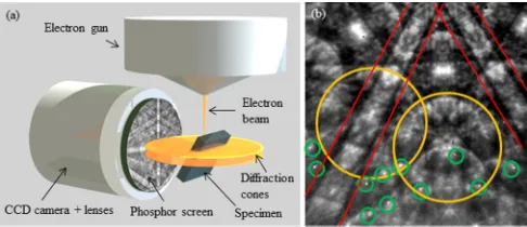
with respect to the exciting electron beam. A digital camera is used to acquire an image of the diffraction pattern formed by the backscattered electrons impinging on the screen [1,4]; this is illustrated in Fig.1(a). The use of the phosphor screen introduces a detrimental conversion of electrons to photons, by the phosphor, and from photons back to electrons by the charge-coupled device (CCD) camera. There are intrinsic light scattering and optical absorption within the phosphor which introduce an intrinsic loss of spatial resolution. This is a limiting factor in applications where it is required to measure small changes in the patterns, for example, in strain measurement [3,5], or where the change in the contrast and sharpness can provide information on the specimen crystalline quality [3,6].
FIG. 1. (Color online) (a) Illustration of the EBSD detection geometry and a conventional EBSD detector. (b) An EBSP from a GaN thin film acquired at an energy of 5 keV, a probe current of ≈1.5 nA, a detector-to-specimen distance of≈10 mm (capture angle ≈60◦), and a 100 s exposure time using the Timepix digital direct electron imaging detector. The red lines outline a pair of Kikuchi bands; the large yellow circles indicate HOLZ rings and the small green circles highlight RHEED spots.
and direction satisfy the Bragg condition, 2dsinθ =nλ, for a set of planes and undergo diffraction, whered is the spacing between planes, θ is the Bragg angle, λ the wavelength of the electron, and n the order of diffraction. Because of the cylindrical symmetry of the Bragg reflection condition with respect to the lattice plane normal, diffraction cones (Kossel cones) are formed. When these cones intersect the phosphor screen, Kikuchi lines are observed in a gnomonic projection; see Fig.1. The Kikuchi lines appear as almost straight lines because the cones are very shallow, as the Bragg angleθ is of order 1°. As each Kikuchi band (pair of Kikuchi lines) is effectively fixed to the plane from which it is formed, an EBSD pattern provides a direct measurement of a sample’s orientation. Rotation of a crystal will produce a rotation of the EBSP; a tilt of a crystal will produce a shift in the EBSP. EBSPs acquired from a mesh of points on a sample can be used to produce a map of tilts or rotations in that sample [1].
The Kikuchi bands are the main features used to extract information from EBSPs in commercial systems, but circlelike features called high-order Laue zone (HOLZ) rings are also observed [4,6]; see Fig. 1(b). The fine structure in HOLZ rings is very energy and lattice-parameter dependent; if these could be recorded with sufficient detail, this could in principle allow the determination of the lattice parameters with very high precision [6,15,16]. Reflection high-energy electron diffraction (RHEED) spots may also appear in the EBSP due to glancing angle coherent scattering of the incident beam. They are visible in the EBSP in Fig.1(b). RHEED patterns may be used to determine a sample’s surface reconstruction and may also provide a precise measure of the lattice constant [17,18].
There is ongoing research to produce a detailed un-derstanding of the physical mechanisms involved in the formation of the diffraction patterns. By using the dynamical theory of diffraction approach it is possible to obtain EBSP simulations showing good agreement with the experimental patterns [7,19,20]. However, the range of energies of the electrons contributing to the EBSP and the depth from
which they emerge from the sample is still not completely understood [6,8,15,21].
To interrogate the energies of the electrons contributing to the EBSPs, energy-resolved EBSPs have been recorded using an electrostatic energy filter placed between the sample and the phosphor screen [22,23], or diffraction band contrast has been measured as function of the electron energy loss [8,24]. An increase in the contrast and sharpness of diffraction features is observed when only electrons having energy close to the primary beam are detected, indicating that the largest contribution to EBSP formation is made by low-loss electrons. High-loss and thus lower-energy electrons appear to give rise predominantly to a featureless background whose effect is a reduction of the diffraction contrast and sharpness in the diffraction pattern.
We can roughly differentiate between three groups of scattered electrons:
(1) Elastically scattered electrons which are either
(1a) coherently elastically scattered (e.g., RHEED spots) or (1b) incoherently quasielastically scattered (through phonon scattering—energy loss typically less than 1 eV).
The number of group (1a) electrons is usually much smaller than group (1b) electrons for a typical EBSD experiment.
(2) Inelastically scattered electrons which have lost only a relatively small amount of energy of the order of typically a few plasmon energies (tens of eV).
(3) Inelastically scattered electrons which have lost sig-nificant energy (several 100 eV). Diffraction effects are exhibited by groups (1) and (2), comprising the low-loss electrons plus elastically scattered electrons. The diffraction effects are gradually diminished for electrons with increasing energy loss in group (2). For more detailed discussion see Refs. [21,23].
In the present work we propose a method for the acquisition of energy-filtered EBSPs where direct electron detection and energy filtering is achieved using a digital complementary metal-oxide semiconductor (CMOS) hybrid pixel detector, Timepix [25]. This approach avoids the use of the phosphor screen and CCD camera combination, and allows energy filtering to be accomplished without any additional hard-ware: the functionality is implemented in the electronics chip.
The advantages of this system include the enabling of a reduction in the electron beam energy, beam current, and acquisition time compared to conventional systems, noiseless acquisition, and most importantly, energy discrimination. This allows the acquisition of small-scale details in the EBSP which are not in practice obtainable with existing commercial EBSD systems. This may provide routes to, for example, the determination of lattice constant, crystal phase identification, and the mapping of strain with greater sensitivity [6,15].
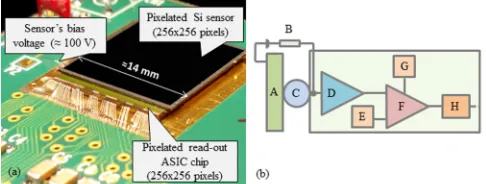
[image:2.608.51.294.70.175.2]FIG. 2. (Color online) (a) Timepix detector, (b) simplified schematic of a detector’s pixel: sensor (A), bias voltage (B), solder bumps (C), preamplifier (D), threshold (E), discriminator (F), threshold adjustment (G), and counter (H).
II. A DIGITAL CMOS HYBRID PIXEL DETECTOR—TIMEPIX
In the last few decades considerable progress has been made in the field of CMOS technology. It is now possible to pack a very large number of components into a very small area, allowing the creation of an application-specific integrated cir-cuit (ASIC), consisting of integrated circir-cuits customized and optimized for a specific rather than general purpose use [27].
Timepix is one of the outcomes of an international collab-oration (Medipix2) hosted at CERN, established to provide a solution for a range of problems in x-ray and gamma-ray imaging [28]. The Timepix detector belongs to the CMOS hybrid pixel detectors family [25,28,29]. The Timepix chip was derived directly from the Medipix2 chip development. It shares most of the properties of the Medipix2 chip, but has additional functionality, in that with the Timepix chip it is possible to obtain timing information (time over threshold and time of arrival). Hybrid pixel detectors such as Timepix can be regarded as digital direct electron detectors. They count events rather than give an output proportional to a fraction of the total energy of the detected particle, as in the case of widely used analog detectors such as CCDs or monolithic active pixel sensors. In the latter case there is variability in the output depending on the path traveled by a detected particle inside the sensor, and there is always intrinsic noise in the device, which reduces the signal-to-noise ratio [27,30].
In the case of a hybrid pixel detector, the sensor and the electronics chip are independent, offering the possibility of the choice of sensor material and sensor thickness depending on the specific application; in the present case the sensor comprises 300µm of silicon. The detector consists of arrays of individual independent counters. Each pixel of the sensor has its own amplification pixel in the electronics chip. Sensor and electronics are composed of 256×256 square pixels, each 55 μm×55 μm in size, covering a global surface of around 1.4 cm×1.4 cm [Fig. 2(a)]; it is also possible to combine chips to obtain a bigger sensor area. Each pixel of the sensor is electrically and mechanically connected, through solder bumps, to the corresponding pixel of the CMOS ASIC electronics chip [25,27].
Each pixel of the electronics is basically composed [see Fig. 2(b)] of a charge sensitive amplifier, a discriminator, and a 14-bit counter [25]. The basic operating principle is as follows: when a particle hits a sensor pixel, a cloud of charges (electron-hole pairs) is generated within the material of the
sensor. The quantity of generated charge is proportional to the total energy deposited within the sensor by the particle. The charges, drifting under the effect of the electric field applied to the sensor, are collected by the solder bump and transferred to the ASIC electronic chip [25]. The signal from the sensor is amplified by the shaping preamplifier and then compared, by the discriminator, with a threshold value. If the signal is greater than the specified threshold value, the discriminator generates a logic signal whose width is proportional to the time for which the voltage at the output of the preamplifier is above the threshold. The global threshold set for the chip can be adjusted individually for each pixel, in order to compensate for small differences between pixels. An equalization of the matrix is typically performed in order to have a more uniform response within the global detector area. If the threshold level is set above the intrinsic noise of the device, it is possible to operate in noise-free conditions [25].
The digital output from the discriminator is processed depending on the acquisition mode of the device. Each pixel of the detector can be individually programmed in order to work in one of the three possible configurations: Medipix, Time Over Threshold, and Time Of Arrival mode [25]. In this article we will describe experimental results from the detector working in Medipix mode. In this mode the device is used as a counter. For each pixel, the internal counter increments one unit every time an electron has energy above the threshold value. Images are recorded using an exposure which does not overflow the maximum pixel counter range (11810 counts per frame), but acquisition in integral mode allows acquisition with virtually infinite dynamic range. The whole chip is read out through a serial (or parallel) interface [25,27]. In our case, the readout operation and data acquisition are managed by a FitPix readout interface and Pixelman software [31–33].
Because in a hybrid pixel technology the sensor is separate from the electronics, there is negligible radiation damage from the incident particle if the energy of the particle is below a specific value [30]. In the range of energies available in a SEM, from 0 to 30 keV, we believe we can completely ignore the problem of radiation damage.
The imaging properties of the detector have been ex-tensively studied [30,34]. Parameters used to define the performance of an imaging detector are the modulation transfer function (MTF), which gives a measure of the spatial frequency response of a detector, and the noise power spectrum (NPS), which describes the spectral component of the noise added to the image by the detection system. These two quantities may be combined to obtain the detective quantum efficiency (DQE). A characteristic value of the DQE is the one at zero spatial frequency, which is referred to as the effective quantum efficiency of the system—see Refs. [30,34] for a detailed description of these parameters.
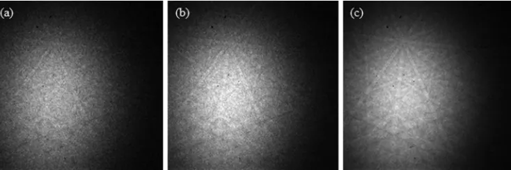
[image:3.608.50.293.71.163.2]FIG. 3. As-acquired EBSPs from GaN for an incident beam energy of 20 keV with a threshold energy of 19.4 keV, a probe current of ≈20 nA, and a detector-to-specimen distance of≈5 mm providing a capture angle of 100°, with an acquisition time of (a) 0.5 ms, (b) 1 ms, and (c) 5 ms.
increase in the MTF, which can reach a value larger than the theoretical value of the MTF obtainable using Nyquist’s sampling theory for a specific pixel pitch [34]. On the other hand, an increase in the threshold level causes an increase in the NPS, with a consequent reduction in the DQE as DQE∝ MTFNPS2. The properties of the Medipix2 chip have been character-ized by Tlustoset al. in Ref. [34]; the MTF and DQE were measured using the spectrum from a 25-keV W tube and a 300-μm-thick silicon sensor. Using a threshold energy of 9.1 keV, they measured a DQE of 25%–26%, which ap-proaches the maximum theoretical value of 27% for the detector. Using a threshold energy of 18.5 keV, the DQE was found to reduce to 5%. The spatial resolution was found to vary between 8.2 line pairs/mm and 11 line pairs/mm for a MTF of 70% for threshold energies between 9.1 and 18.5 keV, respectively [34].
All the characteristics of hybrid pixel detectors as presented above make this family of detectors unique with respect to other currently existing technologies. A more detailed description of the detectors and a comparison between the technologies of different detectors and their performance are described in Refs. [27,30].
III. RESULTS AND DISCUSSION
EBSPs were acquired in an FEI Sirion Schottky field emission scanning electron microscope operating in spot mode. Our detector was positioned in front of a specimen which was tilted so that the sample normal was 70° away from the direction of the incident electron beam. Figure1(b) illustrates the capabilities of the detector in acquiring low-energy EBSPs and shows an EBSP obtained from a single-crystal GaN thin film. This was acquired at an incident electron beam energy of 5 keV, a probe current of≈1.5 nA, a 100-s exposure time, and a detector-to-specimen distance of
≈10 mm which provided a capture angle of≈60◦. Detector-to-specimen distances and capture angles were determined subsequent to measurement by comparison of the acquired EBSPs with dynamical simulations of the EBSPs produced using the Bruker’sESPRIT DYNAMICSsoftware [35]. To date
we have acquired EBSPs at incident electron beam energies down to 3 keV. The EBSP shown in Fig. 1(b) has been flat fielded by dividing the as-acquired EBSP by an image acquired on scanning the beam over a large area of the
sample. Scanning the beam effectively averages out the diffraction information so no diffraction pattern is observed, thus providing a “background” which can be used to flat field the raw EBSP [1].
Acquisition times depend on beam energy, current, the mass and density of the material under study, and the required quality (signal-to-noise ratio) of the EBSP. To date we have acquired EBSPs with the Timepix detector that were of sufficient quality to allow identification of the Kikuchi bands, with acquisition times down to 0.5 ms. Figure3shows examples of as-acquired (i.e., not flat fielded) energy-filtered EBSPs from a single-crystal GaN thin film recorded with acquisition times of 0.5, 1, and 5 ms, respectively. These were obtained at an incident beam energy of 20 keV with a threshold energy of 19.4 keV, a beam current of order 20 nA, and a detector-to-specimen distance of≈5 mm providing a capture angle of≈100◦. In the EBSP acquired with an acquisition time of 0.5 ms [Fig.3(a)], the number of counted electrons is extremely small, even zero at the periphery of the EBSP, due to the angular distribution of the electron intensity. This illustrates that the acquisition time is not limited by the detector but by the available electrons, which is determined by the beam current, and by the angular distribution and energy distribution of backscattered electrons.
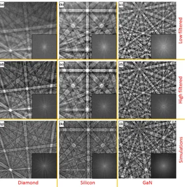
To demonstrate the effect of energy filtering, we acquired EBSPs from diamond, Si, and GaN single-crystal films with an incident electron beam energy of 20 keV, a probe current of ≈10 nA, and detector-to-specimen distances of between
≈8 and 15 mm, which provided capture angles of between
≈80◦ and 50°; these are shown in Fig. 4. These materials were selected to demonstrate the capabilities of the Timepix detector for materials with a range of masses and densities. Flat fielded EBSPs were acquired with the Timepix threshold energy set low (5.5 keV for diamond and GaN and 4.6 keV for Si) and set high and close to the incident beam energy (19.4 keV for all three samples). The threshold energies were subsequently determined through energy calibration of the detector threshold obtained by monitoring the signal on the detector for a range of threshold values and electron beam energies incident on a sample.
FIG. 4. (Color online) (a–c) Experimental EBSPs from diamond, Si, and GaN for an incident beam energy of 20 keV, a probe current of ≈10 nA, and a threshold energy of 4.6 keV. The EBSPs from diamond, Si, and GaN had acquisition times of 0.8, 50, and 10 s, respectively. The insets are two-dimensional (2D) fast Fourier transforms of each image. (d–f) Experimental EBSPs from diamond, Si, and GaN for an incident beam energy of 20 keV, a probe current of≈10 nA, and a threshold energy of 19.4 keV. The EBSPs from diamond, Si, and GaN had acquisition times of 100, 1482, and 60 s, respectively. The insets are 2D fast Fourier transforms of each image. (g–i) 19.5 keV dynamical simulations of EBSPs from diamond, Si, and GaN. The detector-to-specimen distances and capture angles for the EBSPs were estimated by comparison with the simulated EBSPs. For diamond the detector-to-specimen distance was≈8 mm with a capture angle≈80◦, for Si the detector-to-specimen distance was≈15 mm with a capture angle≈50◦, and for GaN the detector-to-specimen distance was≈10 mm with a capture angle≈70◦.
to a given energy is estimated by extrapolation of the curves of Fig. 5 to zero intensity. The inset to Fig. 5 shows the resultant calibration curve of electron energy versus THL which exhibits very good linearity.
The minimum practicable increase in the threshold energy corresponds to one unit of the digital THL value, which corresponds to≈90 eV from the slope of the linear fit.
From the energy calibration performed using x rays by Carramate et al.[36] the energy resolution of the Medipix2 chip has been determined to be of the order of 2 keV [36]. However, Fig.5 illustrates that it is possible to discriminate between curves of detected intensity versus THL for a small change in the electron beam energy (≈200 eV). This implies that while it is not possible to completely resolve energies less than≈2 keV apart, for a given threshold value, electrons with energy less than the corresponding energy are detected with a much lower weight/probability.
The calibration procedure and its comparison with the conventional method (using radioactive sources) will be described in detail in Ref. [37].
For the EBSPs presented in this paper, acquisition times were set significantly higher to provide very high quality patterns for detailed analysis. The acquisition times were set so that for each sample, approximately the same total number of electrons were collected at both low and high threshold energies. The number of electrons, acquisition times, and the ratio of acquisition times are given in TableI.
As shown in Table I, to maintain the same number of collected electrons required an increase of the acquisition time by a factor of ≈125 for diamond, ≈30 for Si, and
[image:5.608.119.492.67.444.2]FIG. 5. (Color online) Threshold calibration using backscattered electrons showing the differentiation of the particle count as a function of the digital threshold value (THL). The inset at the top left shows the energy calibration line derived by extrapolating the intercept to zero of the curves plotted in the main graph.
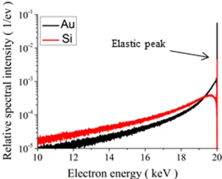
backscattered from light, low-density materials and heavy, dense materials are illustrated in Fig. 6 which shows the Monte Carlo simulations of the backscattered electron energy spectra for Si (atomic weight 30, density 2330 kg m−3) and Au (atomic weight 197, density 19 300 kg m−3), respectively. The simulations use a differential inverse inelastic mean-free-path approach which has been found to predict correctly both the elastic peak at the energy of the primary beam [38], as well as the plasmon loss peaks observed in experiment [8].
The intensities have been scaled so that, for each element the total backscattered intensity from 10 to 20 keV is taken as 1. We can see that Au has a relative elastic peak intensity of 0.055 while for Si it is 0.0045. This means that for Au, 5.5% of the total (10–20 keV) number of electrons is in the elastic peak alone, while for Si it is only around 0.5%. In addition, for Au there is a greater intensity of electrons near the elastic peak than for Si. In general as illustrated in Fig.6, for lighter, less dense materials the backscattered electrons have a much broader energy spectrum; that is, there are more electrons with higher energy loss, so fewer with energy close to that of the incident electron beam. Therefore for a light and low-density material, a longer acquisition time is required to acquire a high-energy-filtered EBSP pattern with a given number of electrons compared to that required for a heavy, dense material.
[image:6.608.64.284.68.225.2]Simulations of EBSPs for diamond, Si, and GaN using the dynamical diffraction theory approach [7] were carried out for
TABLE I. Comparison of acquisition times for diamond, silicon, and GaN samples with change in threshold energy.
Threshold energy
Specimen (keV) Count Acq. time(s) Ratio
Diamond 5.5 7.00×10⁸ 0.8 ≈125
19.4 7.00×10⁸ 100
Silicon 4.6 4.00×10¹⁰ 50 ≈30
19.4 4.00×10¹⁰ 1482
GaN 5.5 6.00×10⁹ 10 ≈6
19.4 6.00×10⁹ 60
FIG. 6. (Color online) Monte Carlo simulations of the backscat-tered electron energy spectra for Si and Au, respectively. The intensities have been scaled so that the backscattered intensity from 10 to 20 keV is taken as 1.
a range of single energies from 18 to 20 keV at intervals of 500 eV. As the energy changes, subtle changes are observed in the EBSPs. For example, the intensity profile of the Kikuchi bands changes (this will be discussed in more detail later in this paper). By comparing the experimental patterns with the simulations, the simulation at an energy of 19.5 keV provided the best match to the EBSPs acquired with high threshold energy, based on the normalized cross correlation coefficient. These are shown in Figs.4(g)–4(i)for diamond, Si, and GaN, respectively.
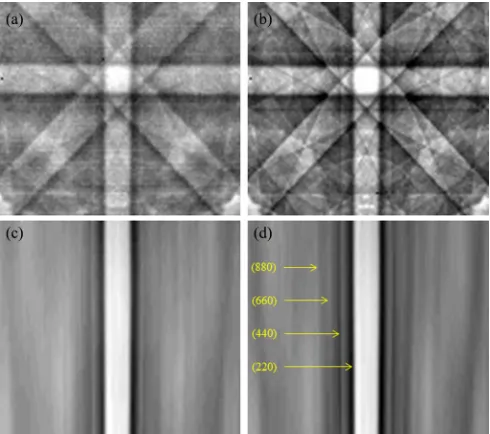
The insets placed at the bottom right of each EBSP in Fig.4 show the power spectrum of the EBSP obtained by performing a two-dimensional fast Fourier transform (FFT) on the pattern. These power spectra provide an indication of the global EBSP quality, that is, a measure of the detail, contrast, and sharpness of the diffraction pattern. A two-dimensional power spectrum is a two-dimensional histogram of the frequency intensity. The lower frequencies are located close to the center of the power spectrum; the frequencies increase with increasing distance from the center. In the power spectra of the EBSP, an increase of the higher-frequency components is observed for the EBSPs acquired at higher threshold energy, indicating that these EBSPs are of higher quality and thus contain more information. For example, HOLZ rings are observed in the high-energy-filtered EBSP from diamond [see Fig.4(d)]—these are not observed in the low-energy-filtered EBSP. Higher-order Kikuchi bands can also be discerned. For GaN fine detail is observable in the HOLZ rings for the high-energy-filtered EBSP [see Fig.4(f)].
[image:6.608.326.544.70.246.2] [image:6.608.49.296.646.751.2]FIG. 7. (Color online) Zoomed-in regions from EBSPs from Si acquired with (a) low threshold and (b) high threshold energies; (c, d) show the extracted (220) and higher-order Kikuchi bands from the EBSPs shown in (a, b), respectively.
can be discerned. The increase in the detail observed in the EBSPs is attributed to the removal of lower energy, i.e., high-loss electrons which, as discussed in the Introduction, give rise to a featureless background. This background obscures the higher-order features; its removal results in EBSPs in which more detail is discernible.
To obtain a measure of the improvement in contrast in the EBSPs on energy filtering, the average contrast was calculated for a Kikuchi band profile for both as-acquired (i.e., not flat fielded) low- and high-energy-filtered EBSPs. The contrast is defined as
C =Maximum band intensity−Minimum band intensity
Minimum band intensity+Maximum band intensity
[image:7.608.51.296.70.287.2]TableIIsummarizes the results obtained for all samples. Note that the greatest change in contrast, on acquiring a high-energy-filtered EBSP, is obtained for diamond. The absolute change in contrast depends on a number of factors including the quality of the sample surface and the position of the detector relative to the sample. The detector’s performance will also vary with threshold energy; for example, at low threshold energy an electron may be counted by more than
TABLE II. Comparison of contrast for low- and high-energy-filtered EBSPs.
Threshold energy
Specimen (keV) Band Contrast Contrast ratio
Diamond 5.5 {220} 0.037 ≈4.0
19.4 {220} 0.149
Silicon 4.6 {220} 0.0304 ≈2.5
19.4 {220} 0.0744
GaN 5.5 {1120} 0.074 ≈2.1
19.4 {1120} 0.159
one pixel [30,40]; this effect will be eliminated at higher threshold energy. The largest change in contrast, however, was always obtained for the diamond sample, while the smallest change in contrast was always obtained for the GaN. This may be attributed to the difference in the energy distribution of backscattered electrons for these materials as discussed previously. For lighter, less dense materials the backscattered electrons have a much broader energy spectrum; that is, there are more electrons with higher energy loss. These electrons contribute to the diffuse background as discussed previously; thus removing these electrons from the EBSP significantly improves the contrast in the pattern. Initially for a given material, care was taken to acquire the same number of electrons for EBSPs recorded at both high and low threshold energies. However, subsequent measurements revealed that, as long as the number of electrons was high enough to obtain an EBSP, the contrast improvement on energy filtering was independent of acquisition time. This is expected since the intrinsic contrast and sharpness of the diffraction pattern should not depend on the counting statistics. High threshold images were acquired for acquisition times of 0.5 s which showed the same improvement in contrast.
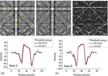
Finally, to further investigate the subtle changes in the diffraction features on energy filtering, the detector was placed further away from the sample and EBSPs acquired with a smaller capture angle of ≈30◦. Figure 8 shows EBSPs (flat fielded) acquired from silicon with an incident electron beam energy of 30 keV, a probe current of ≈2.5 nA, and an acquisition time of ≈100 s. Figure 8(a) shows an EBSP acquired with a low threshold energy, Fig.8(b)shows an EBSP acquired at high threshold energy, and Fig. 8(c) shows the difference between (a) and (b) obtained by first flat fielding the raw EBSPs, normalizing the resultant images, and subtracting (b) from (a).
Note that the difference in the patterns results in asymmetric intensity features on the upper and lower sides of the nonver-tical Kikuchi bands. This may be the result of differences in the contribution of inelastically scattered electrons to each of the differently energy-filtered EBSPs. Close examination of Fig.8(a), the EBSP acquired with the low threshold energy, reveals that the intensity profile of the Kikuchi bands is asymmetric; that is, one side of a band is brighter and the other darker than would be the case for a symmetric intensity profile. This is highlighted by the line profile of band A as shown in Fig.8(d). We believe this excess-deficiency effect is due to anisotropic scattering of inelastic electrons which is a result of the geometry of the measurement and the differential cross section for inelastic scattering [15].
[image:7.608.49.296.646.751.2]FIG. 8. (Color online) EBSPs from silicon for an incident beam energy of 30 keV, a probe current of≈2.5 nA, an acquisition time of ≈100 s, and a detector-to-specimen distance of≈30 mm providing a capture angle of≈30◦. (a) Threshold energy of 4.6 keV, (b) threshold energy of 28.6 keV, (c) difference between (a) and (b), (d) mean Kikuchi band profile for band A in (a), (e) mean Kikuchi band profile for band B in (a), where the energy-dependent effect is much smaller than for band A.
reveals the energy dependence of the excess-deficiency effect across the EBSP. This effect is also visible in other features of the patterns, such as the edge of the HOLZ ring and the intersection of the Kikuchi bands, as indicated by the bright features (indicating large differences between the two patterns) in Fig.8(c). To explain this unexpected observation requires a quantitative model describing the development of diffraction effects with energy loss. This involves the simultaneous treatment of the multiple inelastic scattering in the sample and dynamical diffraction effects, as has been outlined by Dudarev et al. using the density matrix formalism [41]. Our observations indicate that the details of the interrelated multiple inelastic scattering and dynamical diffraction are not completely understood and should thus provide a stimulus for an improved theoretical treatment which, while beyond our current capabilities, will be the focus of future work.
IV. SUMMARY
To summarize, we have shown that digital energy filtering allows the acquistion of EBSPs exhibiting enhanced detail and contrast. The improvement in the quality of EBSPs is greatest for light, less dense, materials. This is attributable to the removal of electrons which contribute to a diffuse
background and not to the diffraction pattern. This allows for example, the detection of high-order diffraction features. In addition comparison of low- and high-energy-filtered EBSPs implies that inelastically scattered electrons make a significant contribution to the appearance of the diffraction features in the EBSPs. The observed excess-deficiency effects are supressed on high-energy threshold filtering of the EBSPs. The ability to energy filter EBSPs will allow us to not only obtain a better understanding of the formation of EBSPs but also widen the application of EBSD to new materials and to new applications.
ACKNOWLEDGMENTS
We would like to thank Peter Parbrook, Tyndall National Institute, University College, Cork, Ireland for providing us with the GaN sample and Alexandre Tallaire, Laboratoire des Sciences des Proc´ed´es et des Mat´eriaux LSPM-CNRS, Universit´e Paris 13, France for providing the diamond sample. We would like to thank NPL for partial funding of Ste-fano Vespucci’s Ph.D. studentship. This work was carried out with the support of EPSRC Grant No. EP/J015792/1. The experimental data presented in this paper is avail-able at http://dx.doi.org/10.15129/7e864c9e-516c-465d-993d-b271f3698e1bor from the corresponding author.
[1] R. A. Schwarzer, D. P. Field, B. L. Adams, M. Kumar, and A. J. Schwartz, inElectron Backscatter Diffraction in Materials Science, edited byA. J. Schwartz, M. Kumar, B. L. Adams, and D. P. Field (Springer, New York, 2009), Vol. 2, Chap. 1, p. 1.
[image:8.608.119.490.68.330.2][3] A. J. Wilkinson,J. Electron Microsc.49,299(2000).
[4] A. P. Day, in Electron Backscatter Diffraction in Materials Science, edited by A. J. Schwartz, M. Kumar, B. L. Adams, and D. P. Field (Springer, New York, 2009), Vol. 2, Chap. 5, p. 65.
[5] A. J. Wilkinson, D. J. Dingley, and G. Meaden, inElectron Backscatter Diffraction in Materials Science, edited by A. J. Schwartz, M. Kumar, B. L. Adams, and D. P. Field (Springer, New York, 2009), Vol. 2, Chap. 17, p. 231.
[6] A. Winkelmann, inElectron Backscatter Diffraction in Materi-als Science, edited byA. J. Schwartz, M. Kumar, B. L. Adams, and D. P. Field (Springer, New York, 2009), Vol. 2, Chap. 2, p. 21.
[7] A. Winkelmann, C. Trager-Cowan, F. Sweeney, A. P. Day, and P. Parbrook,Ultramicroscopy107,414(2007).
[8] A. Winkelmann, K. Aizel, and M. Vos,New J. Phys.12,053001 (2010).
[9] O. C. Wells,Scanning21,368(1999).
[10] T. Matsukawa, R. Shimizu, and H. Hashimoto,J. Phys. D: Appl. Phys.7,695(1974).
[11] G. E. Lloyd,Mineral. Mag.51,3(1987).
[12] F. Yubero, N. Pauly, A. Dubus, and S. Tougaard,Phys. Rev. B 77,245405(2008).
[13] A. Winkelmann, F. Salvat-Pujol, and W. Werner, Microsc. Microanal.19, 738 (2013).
[14] S. Zaefferer and N. N. Elhami,Acta Mater.75,20(2014). [15] A. Winkelmann,Ultramicroscopy108,1546(2008).
[16] J. R. Michael and J. A. Eades, Ultramicroscopy 81, 67 (2000).
[17] A. Ichimiya and P. I. Cohen, Reflection High-Energy Elec-tron Diffraction (Cambridge University Press, Cambridge, 2004).
[18] K. Z. Baba-Kishi,Ultramicroscopy34,205(1990).
[19] P. G. Callahan and M. De Graef,Microsc. Microanal.19,1255 (2013).
[20] S. Villert, C. Maurice, C. Wyon, and R. Fortunier,J. Microsc. 233,290(2009).
[21] A. Winkelmann,J. Microsc.239,32(2010).
[22] A. J. Eades, A. Deal, A. Bhattacharyya, and T. Hooghan, in Electron Backscatter Diffraction in Materials Science, edited byA. J. Schwartz, M. Kumar, B. L. Adams, and D. P. Field (Springer, New York, 2009), Vol. 2, Chap. 4, p. 53.
[23] A. Deal, T. Hooghan, and A. Eades,Ultramicroscopy108,116 (2008).
[24] A. Winkelmann and M. Vos,Ultramicroscopy125,66(2013). [25] X. Llopart, R. Ballabriga, M. Campbell, L. Tlustos, and W.
Wong, Nucl. Instrum. Methods Phys. Res., Sect. A581, 485 (2007).
[26] A. J. Wilkinson, G. Moldovan, T. B. Britton, A. Bewick, R. Clough, and A. I. Kirkland, Phys. Rev. Lett. 111, 065506 (2013).
[27] A. R. Faruqi and R. Henderson,Curr. Opin. Struct. Biol.17,549 (2007).
[28]http://medipix.web.cern.ch/medipix/
[29] X. Llopart, M. Campbell, R. Dinapoli, D. San Segundo, and E. Pernigotti,IEEE Trans.Nucl. Sci.49,2279(2002).
[30] G. McMullan, D. M. Cattermole, S. Chen, R. Henderson, X. Llopart, C. Summerfield, L. Tlustos, and A. R. Farugi, Ultramicroscopy107,401(2007).
[31] V. Kraus, M. Holik, J. Jakubek, M. Kroupa, P. Soukup, and Z. Vykydal,J. Instrum.6,C01079(2011).
[32] T. Holy, J. Jakubek, S. Pospisil, J. Uher, D. Vavr´ık, and Z. Vykydal,Nucl. Instrum. Methods Phys. Res., Sect. A563,254 (2006).
[33]http://aladdin.utef.cvut.cz/ofat/others/Pixelman/Pixelman.html [34] L. Tlustos, R. Ballabriga, M. Campbell, E. Heijne, K. Kincade,
X. Llopart, and P. Stejskal, IEEE Trans. Nucl. Sci.53, 367 (2006).
[35] http://www.bruker.com/products/x-ray-diffraction-and- elemental-analysis/eds-wds-ebsd-sem-micro-xrf-and-sem-micro-ct/esprit-dynamics/overview.html.
[36] L. F. N. D. Carramate, F. Nachtrab, M. Firsching, A. L. M. Silva, A. M. da Silva, J. F. C. A. Veloso, and N. Uhlmann,J. Instrum. 8,C03022(2013).
[37] S. Vespucci, Ph.D. thesis, Dept. of Physics, University of Strathclyde (to be published 2016).
[38] F. Salvat-Pujol, and W. S. Werner,Surf. Interface Anal.45,873 (2013).
[39] F. Ram, S. Zaefferer, and D. Raabe,J. Appl. Crystallogr.47,264 (2014).
[40] G. McMullan, S. Chen, R. Henderson, and A. R. Farugi, Ultramicroscopy109,1126(2009).