3'// L
.... ," r l_"
~ r i';
L/ \
CODE IDENT
CONTR NO.DR BV CHK BY
REVIEW ENGINEER
REV.
A
REVISIONS
PROD REL PER ECO #0986
./
. 'FUNTION AL SPECIFICA TION
CPU32/25 APPLICATION PROCESSOR
A
DWG.NO.
FS-02204-XX
~fc·
REV
A
ARIX CORPORATION
CPU32/25 Application Processor
Functional Description
Part
Number FS-02204-XX
Revision A
Copyright 1988
ARIX Corporation
February 1988
Copyright © 1988, ARIX Corporation.
This document contains the latest information available at the time of preparation. Therefore, it may contain descriptions of functions not implemented at manual distribution time. To ensure that you have the latest information regarding levels of implementation and functional availability, please consult the appropriate release documentation or contact your local ARIX representative.
ARIX reserves the right to modify or revise the content of this document. No contractual obligation by ARIX regarding level, scope, or timing of functional implementation is either expressed or implied in this document. It is further understood that in consideration of the receipt or purchase of this document, the recipient or purchaser agrees not to reproduce or copy it by any means whatsoever, not to permit such action by others, for any purpose without prior written permission from ARIX.
UNIX is a registered trademark of AT&T.
•
Preface
Preface
This functional specification describes the CPU32/25 Application Processor board. This board contains a full 32-bit Motorola MC68020 microprocessor and runs at 25 MHz.
This document is divided into six sections as follows:
Section 1 Introduction - A general introduction of the CPU32/25 board. Section 2 Functional Characteristics - Describes the characteristics and
specifications of the CPU32/25 board.
Section 3 Functional Overview - Describes how the CPU32/25 operates in an ARIX system.
Section 4 CPU32/25 Programmer's Model - Provides information about memory, the MMU, ICB registers, and CPU peripherals within the CPU32/25 board.
Section 5 Interface Description - Describes the plugs used to interface between the CPU32/25 and an ARIX system.
Preface
Table of Contents
Section 1 Introduction ... . 1-1
MC68020 Microprocessor ... 1-1
Cache Memory... ... ... ... ... ... ... .... 1-2 Diagnostics ... ... 1-2
Memory Management . .... ... ... ... ... 1-2
Configurations ... 1-2
Section 2 Functional Characteristics ... . 2-1 Specifications ... ... 2-1
Section 3 Functional Overview ... ... . 3-1
CPU32/25 Functional Elements ... ... ... ... .... 3-1
Slave's Mailbox ... .... .... ... ... ... 3-10
ICB and PMB Bus Operation ... 3-12
Section 4 CPU32/25 Programmer's Model .. ... . 4-1 Memory ... 4-1
MMU Registers ... 4-3
ICB Registers ... 4-8 Peripherals ... 4-9
ICB Programming Considerations .. ... ... ... 4-11
MC68881 Coprocessor Programming Considerations .... 4-14
Section 5 Interface Description ... . 5-1
Figure 1-1 Figure 3-1 Figure 3-2 Figure 3-3 Figure 3-4 Figure 3-5 Figure 3-6 Figure 3-7 Figure 3-8 Figure 5-1 Figure 5-2 Figure 5-3 Figure 5-4 Figure 5-5
Preface
List of Figures
CPU32/25 Block Diagram .. ... ... ... ... 1-3 Cache Fill: Read Virtual 0 And Physical 0 . ... 3-6 Cache Fill: Read Virtual 1000 And Physical 0 ... 3-6 Cache Fill: Read Virtual 2000 And Physical 0 ... 3-7 Cache Fill: Read Virtual 3000 And Physical 0 ... ... 3-7 Cache Fill: Read Virtual 0 And Physical 0 ... 3-8 Cache Fill: Read Virtual 0 And Physical 1000 ... 3-8 Cache Fill: Read Virtual 0 And Physical 2000 ... 3-9 Cache Fill: Read Virtual 0 and Physical 3000 ... 3-9 Plug One .. ... ... .... ... ... ... .... ... ... ... 5-3 Plug Two ... ... ... ... ... .... ... ... 5-5 Plug Three ... ... ... .... ... ... .... ... ... ... ... ... 5-7 Jack Four ... ... 5-8 Jack Five ... ... ... ... ... ... ... .... ... ... ... ... 5-9
Section 1
Introduction
Section 1
Introduction
The ARIX CPU32/25 Application Processor board provides a substantial increase in processing power to the ARIX Series 1000. This board combines a full 32-bit Motorola MC68020 microprocessor and a MC68881 floating-point coprocessor.
In this application, the MC68020 operates at the full 25 MHz clock speed and drives a full 32-bit data path. The MC68881 floating point coprocessor performs math functions handed off by the MC68020. This shared-processing concept greatly reduces wait states and the amount of time required to run a given job. A single ARIX 850 system may contain up to three of these 25 MHz MC68020 Application Processor boards; and an ARIX 825 system may contain up to two boards. In addition to having its own MC68020 microprocessor and MC68881 coprocessor, each board contains 64 Kbytes of high-speed cache· memory without wait states, an MMU (Memory Management Unit), a battery-backed hardware clock, a console port, a diagnostic port, and EPROM based self-diagnostics and boot routines. Each Application Processor board operates independently of the others, and shares a common pool of memory (up to 64 megabytes) over a high-speed 32 bit Processor Memory Bus.
MC68020 MICROPROCESSOR
The MC68020 provides a full 32-bit data path to complement the 32-bit internal data structure. In addition, it features sixteen 32-bit general purpose and five special-purpose control registers, and a 32-bit program counter. It also includes a co-processor interface, eighteen addressing modes and a high performance 128 word on-chip instruction cache. The MC68020 instruction set has been especially designed for high-level languages and ARIX, which is Arete's implementation of UNIX® 5.2 for tightly-coupled shared-memory, multi-processor systems.
•
Introduction
Section 1
CACHE MEMORY
Cache memory for the Areta Application Processor cache permits it to run at full clock speed, since no wait states are incurred. Working out of cache reduces bus traffic and further improves system throughput. All reads from memory (whether instructions or data) are directed to cache memory; all writes to cache memory are written through to maintain cache concurrency throughout the system. Redundant tag bits are provided for both memory and the Application Processor, thus allowing monitoring of the Processor Memory Bus for invalidations without wait states.
DIAGNOSTICS
In addition to console support and a set of diagnostic LEOs on the front edge of the board, each Application Processor includes a status register, which allows it to continuously monitor environmental and power status of the system. Power on confidence tests are run from onboard EPROMs that perform a complete checkout of the Application Processor, automatic polling to check system configuration, and testing of the bus interfaces. A monitor is included for on-line debugging after the diagnostics detect a failure.
MEM·ORY MANAGEMENT
The Areta system provides two-level mapping to allow scatter loading of processes, and multiple protection modes. Physical memory pages are four Kbytes in size and may be set for read, write, code, data and page ownership protection within the MMU. The MMU has been enhanced to support a larger virtual and physical memory space than the previous Application Processor offerings.
CONFIGURATIONS
Any Application Processor within a single cabinet may function as the Master Processor, by a simple switch selection. A load-balancing algorithm inherent to the Areta, allows all of the Application Processors (whether master or slave) to fully share the processing load.
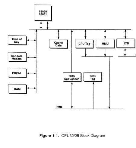
CPU32/25
BLOCK DIAGRAM
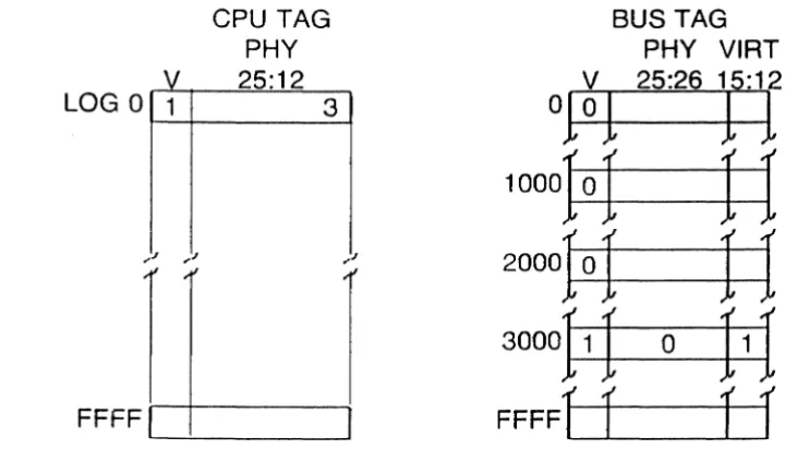
A block diagram of the CPU32/25 is shown in Figure 1-1.
Section 1
Introduction
68020 68881
!l-I
Time of,
I
Day
I
Cache CPU Tag MMUI
ICB Datal
Console IcaModem
I
PROMI
BUS BUSI
Sequencer Tag
!I-RAM
[image:9.635.69.521.144.637.2]PMB
Figure 1-1. CPU32/25 Block Diagram
..
Section 2
Functional Characteristics
Section 2
Functional Characteristics
The CPU32/25 Application Processor board, running at 25 MHz, provides a substantial increase in performance over the CPU32 Application Processor board, which runs at 12.5 MHz. In addition, the integral cache memory for the ARIX CPU32/25 Application Processor board permits it to run at the full 25 MHz clock speed, since no wait states are incurred for most cycles. The use of cache memory significantly reduces bus traffic to provide a further improvement in system throughput.
The MC68881 Coprocessor further extends the processing power of the system by performing computations handed off from the MC68020/25.
SPECIFICATIONS
Specifications for the CPU32/25 Application Processor board are shown in the following table:
MC68020 SPECIFICATIONS
Processor 32 bit MC68020 running at 25 MHz Cache 64 Kbytes (no wait states) 35 ns Address Space 64 MB
Memory Management Proprietary Hardware Map Page Size 4 Kbytes
Floating-Point MC68881 Coprocessor
Clock/Calendar Battery Supported, accuracy within 10 ppm Diagnostics EPROM based Start-up Board level
Dimensions 14.437 inches (366.7 mm) x 15.75 inches (400 mm) Connections DIN 41612 Plug and Socket
*
Section 3
Functional Overview
Section 3
Functional
Overview
This section provides a functional overview of the ARIX CPU32/25 Application Processor board. The individual elements of the board and the functions and interrelationships are described.
Motorola MC68020 32-Bit Microprocessor
In this application, the Motorola MC68020 microprocessor chip is defined as the CPU. The MC68020 has a full 32-bit data path. It executes at 25 MHz with no wait states on most cycles.
Motorola microprocessor Math Processor
The Motorola microprocessor Math or Floating-POint Coprocessor is physically a separate device, but it should be considered to be part of the MC68020, as they function as a single functional unit. In normal operation, the MC68020 fetches instructions and operands, and hands off the math-related operations to the microprocessor. The microprocessor never takes control of the bus.
CPU32/25 FUNCTIONAL ELEMENTS
The individual functional elements in the Application Processor are as follows:
Primary Map
The primary mapper adds an offset value to the high order 10 bits of the logical address for the CPU. The sum indexes an entry in the secondary map. The offset value for a process is contained in a register, which the supervisor may load at any time. This allows for a fast context switch between processes.
There is one offset value for user processes, and one for the supervisor. The selection of which offset to use is made automatically at the beginning of each bus cycle.
Functional Overview
Section 3
Secondary Map
The secondary map uses the map index from the primary map to look up a page entry. The page entry contains a physical memory page number and some attribute information for that physical page.
Physical Page Number
The CPU32/25 board can address 64 megabytes (MB) of physical memory. The pages contain 4 kilobytes (KB) each, and there are 16,384 of them. Therefore, there are 14 bits of address in a page number.
Page Attributes
Each page entry has a process 10, some protections, and some statistics. The operating system may enable faults that can abort a process based on this data.
Process /0. The process 10 is compared against a value in the appropriate (user or supervisor) process 10 register.
Code Page Attribute. This bit identifies a page as executable only. Operand access of a code page or execution of a non-code page may fault a process.
Cacheab/e Attribute. This bit enables cache-load. In normal operation, all pages are cacheable.
Written Statistic. If statistic updating is enabled, then this bit is set by writing any location in the page.
Accessed Statistic. If statistic updating is enabled, then this bit is set whenever its page is accessed. The two statistics may be useful for page-replacement algorithms in a virtual memory operating system.
Write Protect Attribute. Set this bit to write protect the page. Clock Stretching
In order for the MMU to translate an address for the CPU a wait state must be incurred. To minimize the impact of this all MMU outputs are latched, a set for code and a set for data, and the previous cycle's page descriptor information is used unless a 4k page boundary is crossed. If a 4k boundary is crossed, the CPU clock gets stretched, the latches are updated and the CPU cycle terminates with effectively one wait state. Based on CPU trace data the wait state will only happen on an average of once every 14 cpu bus cycles.
•
Section 3
Functional Overview
Cache Memory
CPU32-25 has a 64K single set cache. There are two sets of tag memory, one for the CPU and one used to monitor the bus. Along with the data store and tags there is one more functional block, a FIFO is used to pass addresses from the bus tag to the CPU tag for invalidation.
The cache implementation on this board is a hybrid of a virtual and physical design. The CPU tag and data store resemble a virtual cache because they are indexed by logical addresses. The bus tag appears as a physical cache because it is indexed by physical addresses. Likewise the tag information is made up of physical addresses. If the MMU page size were as big as the cache this could have been just a physical cache. The cache size is 64k and the page size is 4k. This means A 11-0 virtual are the same as A 11-0 physical. However virtual A 15-12 won't necessarily be the same as physical A 15-12. This leaves two special cases that must be dealt with:
1 . Two different virtual addresses point to the same physical address. When this situation occurs, the cache entry created by the first virtual address must be invalidated before the second is filled. This invalidation is done on the CPU tag. If this invalidation case wasn't done the CPU would read incorrect data.
2. Two different physical addresses pointed to by the same virtual address. When this situation occurs, the cache entry created by the first physical address must be invalidated before the second is filled. This invalidation is done on the bus tag. Unlike the previous case, if this invalidation wasn't done it would cause extra spy invalidations and decrease the effective cache size but the CPU would still operate properly.
There are six basic types of cycles the cache has to deal with. The CPU can have read hit and misses and write hit and misses. The bus tag can have PMB bus write hit and misses only. In addition, the two tags and data store can be directly accessed by the CPU as ram for diagnostics. In the following text I will describe each type of cycle. Keep in mind that the goal of the invalidations, in the CPU cycles, is to keep a one to one relationship between the two tags.
The block or line size is 4 bytes which means each set of tag memory has 16K entries.
The following is the bit definition of the functional blocks: CPU tag contains physical A25-12 and a valid bit. BUS tag contains physical A25-16 and virtual A 15-12 and a valid bit. The F.IFO contains physical A25-16 and virtual A 15-12 from the bus tag data. The data store contains 031-0.
Both tags are addressed by multiple sources depending on the type of cycle being executed. The data store is indexed by virtual A 15-0.
Functional Overview
Section 3
CPU read hit
L
When the CPU starts a read cycle, the data store and CPU tag are both looked up. The CPU tag is compared to the current_ph~sicC!1 address, and produce match bits that go to the buss error and halt logic. If the bits are a match, the CPU terminates the bus cycle and takes the data from the data store.
CPU Read Miss
When the CPU starts a read cycle, the data store and CPU tag are both looked up. The CPU tag is compared to the current .e.hysic~ address, and produce match bits that go to the buss error and halt logic. If the bits don't match, both buss error and halt are asserted which causes a CPU rerun cycle. A rerun cycle initiates a cache fill sequence. During the rerun cycle a main memory cycle is requested, and the CPU waits until the data is returned.
While the CPU is waiting for the PMB bus cycle to complete,the two invalidations previousLy mentioned take place. The CPU tag uses the current A 11-0 and virtual A 15-12 from the bus tag to invalidate a location. The bus tag uses the current A 11-0 and physical A 15-12 from the CPU tag to invalidate a location. When the PMB memory bus signals done, the CPU bus cycle is terminated and data is taken from the memory bus data latches. At the same time the data store writes that data into its memory. Also, the CPU tag is written with that bus cycles physical address and the bus tag is written with those physical and virtual address bits it uses.
CPU Write Hit
Unlike CPU read cycles, writes don't generate rerun cycles. Write cycles take wait states until the write accelerator is empty, and if empty, no wait states are needed. When the CPU starts a write cycle, the data store and CPU tag are both looked up. The CPU tag is compared to the current 1?hysic~~ddress, if there is a match the data is written to the write accelerator and the data store. Notice that no tag manipulation is done and a write doesn't ever cause a cache fill sequence. Another thing to note is after a write hit, the data store needs one additional clock to write the new data. Therefore, if a CPU cycle comes out in the minimum amount of time after a write hit, a wait state will be taken.
OOGS\\JlT
S '
tJ (,. l~ ~y\'
!&
<)ARIX Corporation 3-4
A
b
~
C7
b
OS/f1~ln
tS
~
Section 3
Functional Overview
CPU Write Miss
When the CPU starts a write cycle, the data store and CPU tag are both looked up. The CPU tag is compared to the current physical address, if there isn't a match the data is written to the write accelerator only. All write misses are spied upon just like any other PMB bus write initiated by another bus master. This is to prevent special case number 1 from above, having two virtual entries for one physical location.
Bus Write Hit
...
When a PMB bus write cycle is started, the bus tag data is looked up and the physical address bits and the current address on the PMB bus are compared. If there is a match, the physical address A25-16 and virtual A 15-12 from the bus tag are loaded into the fifo. At this time that location in the bus tag is invalidated arid some short time later the CPU tag will use the address in the fifo to invalidate that location.
Bus Write Miss
When a PMB bus write cycle is started, the bus tag data is looked up and the physical address bits and the current address on the PMB bus are compared. If there is isn't a match, no action is taken.
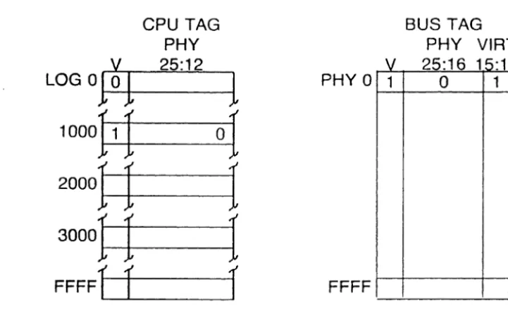
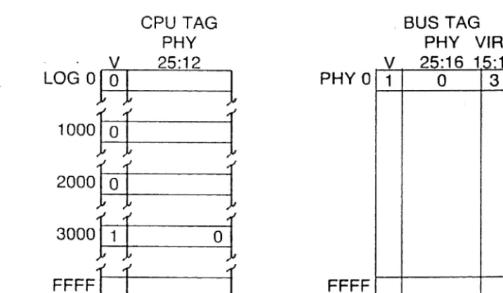
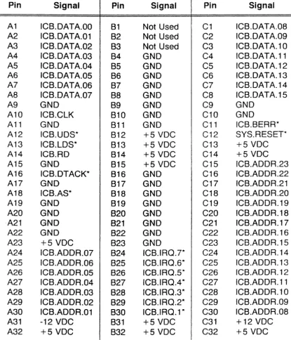
Figures 3-1 to 3-4 show the contents of the CPU and BUS tags for consecutive cache fills. This example shows the virtual address changing while pointing to the same physical address.
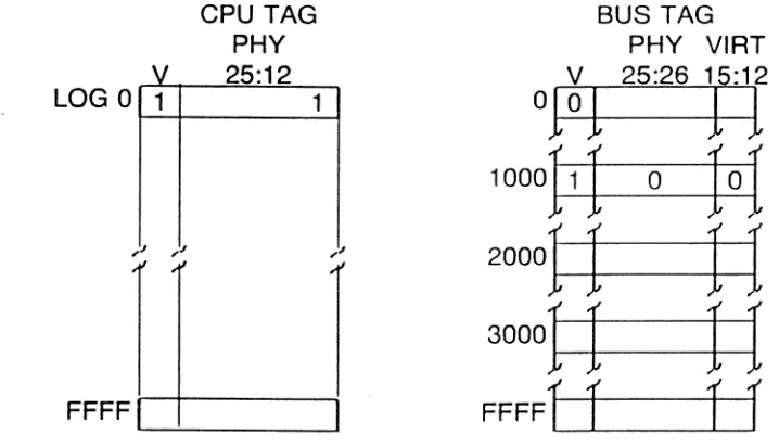
Figures 3-5 to 3-8 show the contents of the CPU and BUS tags for consecutive cache fills. This example shows the virtual address remaining the same while the physical address changes.
Functional Overview
CPU TAG PHY V 25:12
LOG °1 1 1 °1
1000
11
1
2000
11
1
3000
11
1
FFFFl
f
r
V
PHYO 1
FFFF
BUS TAG PHY VIRT
25:16 15:12
[image:16.624.137.463.113.323.2] [image:16.624.103.464.391.610.2]° °
Figure 3-1. Cache Fill: Read Virtual
°
And Physical°
CPU TAG BUS TAG
PHY PHY VIRT
V 25:12 V 25:16 15:1?
LOG 0101
1
PHYO 1 ° 1
1000
1
11
012000
11
I
3000
11
I
FFFF1
f
r
FFFFFigure 3-2. Cache Fill: Read Virtual 1000 And Physical °
Section 3
Section 3
CPU TAG PHY V 25:12
LOG 010
1
1
1000101
I
2000111
01
300011
1
FFFF
1
r
r
PHY
a
FFFF
Functional Overview
V
1
BUS TAG PHY VIRT
25:16 15:12
a
2Figure 3-3. Cache Fill: Read Virtual 2000 And Physical
a
CPU TAG BUS TAG
PHY PHY VIRT
V 25:12 V 25:16 15:12
LOG 010
1
1
PHYa
1 0 3100010
I
1
200010
I
1
3000111
01
[image:17.626.136.460.113.321.2]FFFFl
1
r
FFFFFigure 3-4. Cache Fill: Read Virtual 3000 And Physical 0
[image:17.626.104.462.394.602.2]..
Functional Overview
Section 3
CPU TAG BUS TAG
PHY PHY VIRT
V 25:12 V 25:26 15:12
LOG 0 1 0
01 1
1
01°1
1000
11 1 1
2000
11 1 1
~'J ,'J ,~
."
3000
11 1 1
[image:18.612.127.458.112.320.2]FFFF FFFFl
r
f
r
Figure 3-5. Cache Fill: Read Virtual
°
And Physical°
CPU TAG BUS TAG
PHY PHY VIRT
V 25:12 V 25:26 15:12
LOGO 1 1
°1°1
1 1
1000
1
11
°
1
01
2000
11 1 1
,~ ;'~ ,~
'I 'I
"
3000
11 1 1
FFFF FFFFl
r
f
r
Figure 3-6. Cache Fill: Read Virtual
°
And Physical 1000 [image:18.612.100.459.394.600.2]Section 3
Functional Overview
CPU TAG BUS TAG
PHY PHY VIRT
V 25:12 V 25:26 15:12
LOG
°
1 2°1°1
I 1
100010 1 1
1
2000111
101
~'J .;oJ ~J
°
1
1
300011
1 1
[image:19.615.135.471.109.325.2]FFFFl
f
f ]
FFFFFigure 3-7. Cache Fill: Read Virtual
°
And Physical 2000 CPU TAG BUS TAGPHY PHY VIRT
V 25:12 V 25:26 15:12
LOG
°
1 3°1°1
1 1
100010 1 1
1
200010 1 1 1
,.'J "J ~J
tI
3000111
°
111
FFFF FFFFl
f
f
r
Figure 3-8. Cache Fill: Read Virtual
°
and Physical 3000 [image:19.615.107.467.392.598.2]Functional Overview
Section 3
CPU32 Master Operation
All CPU32/25 Application Processor boards have the same Interprocess Communications Bus (1GB) circuitry installed, but some of it is only enabled on the master. A set of data transceivers and address buffers drive the bus only when the master GPU selects the 1GB address range. The selected 1GB slave drives ICB.OTACK to terminate the cycle. A timer terminates an unacknowledged ICB cycle after about 40 microseconds (40 fJ.s). An ICB timeout under these conditions results in a bus error.
CPU32 Slave Operation
Each CPU32/25 Application Processor board has ICB slave circuitry. The master CPU controls the slaves through it. If the board is not designated as a master, the board defaults to slave operation. This slave circuitry is selected when the high-order ICB address bits < 16 ... 23> match the slot number where the board is installed.
SLAVE'S MAILBOX
The bytewide register (ICB command) may be written into by the master. The slave may rE!ad it at any time, but normally it reads leB command in response to the slave interrupt flag.
Another bytewide register (1GB status) may be written by the slave and read by the master. An interrupt request flag (set by the slave at any time and cleared when the master reads 1GB status) is normally used to get the master to read it.
Another byte of 1GB status may be read by the master. (The master may read both as a word.) This byte returns the board 10, and the status of the two 1GB interrupt flags.
Slave Controls
A slave configuration register gives the master total control. The master can write a byte at any time. This register is cleared by a system reset (power-up, pushbutton, or master executing RESET instruction).
Two bits let the '!laster control the slave's HALT and RESET lines. To reset the slave, the master must clear both bits, wait 10 microseconds, then set them both. Two more bits control the PMB priority level the slave will use. Three bits control the 1GB interrupt request level the slave will assert. One bit, when set, causes a slave interrupt. The slave can clear this bit by reading its mailbox.
Section 3
Functional Overview
Ports
Ports provided on the CPU32/25 include serial ports, a timer, and a clock/calendar device.
Serial Ports
Serial ports are provided by a Zilog 8031. This device has two serial (asynchronous) channels. One is designated "console," and the other "modem," but they are identical, pin for pin. They can connect to an RS-232 terminal using the ARIX console cable supplied with the system. The two connectors are mounted on the front edge of the MC68020 board, below the LEOs. These serial ports have their own built in bit-rate (baud) generators.
Timers
The timer function is provided by a Zilog 8036. This device has three timers, and some parallel I/O lines. One timer is the 60 Hz interrupt, and the other two are spare. The parallel I/O is used to access the calendar device.
Clock/Calendar
The clock/calendar function is provided by an OKI 58321 device. This device has its own battery back-up and runs at all times. It keeps time in BCD format, with a separate register for each digit.
Functional Overview
Section 3
ICB AND PMB BUS OPERATION
The subsections that follow describe how the ICB and PMB buses operate.
ICB
The ICB connects to all boards in the system. If more than one CPU is configured In a system, one CPU is designated as the master. The master CPU controls the ICB, using it to control the operation of the slave CPUs, and to monitor their status. The ICB reads and writes the OTB master 10 arbiter RAM. Note that each board slot connects to the ICB in the ARIX Series 1000 system, and has a unique 64 Kbyte segment of memory. Status and control registers for the board are located at the top of its memory segment. Each slot has a 5 bit hardwired slot address that determines which 64 Kbyte memory segment the board occupies. Another location in the input/output segment, read through the ICB, gives the board type currently in that slot. At power up, the master CPU reads the board type from each slot, so the system can configure itself automatically. The ICB has 16 data bits, 21 address bits, and a subset of the VME bus control signals.
ICB Data Buffers, Control
The 16-bit ICB data bus (ICB.DATA.0-15) is buffered with bidirectional transceivers. These devices are enabled when ICB address bits 16 through 20 match the slot address, the ICB address strobe (ICB.AS"') is active, and one or both of the ICB data strobes (ICB.LOS", ICB.UOS") are active. The direction of the buffers is determined by the ICB read signal, ICB.RO.
I/O Decoders
The first level of address decoding is comparing the five bit board slot address with ICB address bits 16 through 20. If they match and ICB.AS" is valid, then ICB.SEL" is activated. Address bits 21 through 23 are not currently used and are pulled to logic level 1.
PMB
The PMB provides the 32-bit data path between main memory and the CPUs and OMA channels in the system. Up to three CPUs can dynamically share up to 64 megabytes of main memory on the PMB. The PMB includes 32 bits of data, 26 address bits, and control signals.
Section 3
Functional Overview
PMB Bus Arbiter
The PMB bus arbiter on the DMC accepts requests for use of the PMB by the various PMB bus masters. The highest priority requester is then granted use of the bus to transfer data to or from main memory. There are six request inputs for the PMB: 4 CPU requests, 1 DMA request (for the up to four DMA channels), and the refresh request. Following is a list of the PMB request priorities:
Device PMB Request Priority Refresh
a
(highest)DMA channels 0-3 1
CPU 0 2
CPU 1 3
CPU 2 4
CPU 3 5 (lowest)
These requests are activated on the rising edge of the PMB clock (25 MHz) by the various bus requesters, and are then synchronized again on the DMC by the PMB clock. The PMB arbiter uses one set of request and grant signals to interface with the four DMA channels.
The signal PMB.GO is active for the first five cycles of any PMB cycle, except in the case of a 32-bit write, where it is active for six cycles. The requester must not drive the PMB bus once its grant has been deactivated.
The PMB.CYC.DONE* signal is activated after the appropriate number of clock periods have elapsed to indicate the completion of the cycle. The following chart shows the number of PMB clock cycles, or states, required for each type of cycle:
Type of Cycle Number of Cycles PMB States
Refresh 8 80 - 87
32 bit write 8 80 - 87 Read with no error 10 80 - S9 Read with error 13 SO - S12 Read/Modify/Write 15 SO - 814
Functional Overview
Section 3
The Read/ModifylWrite cycle mayor may not be associated with an error condition. It
is handled in the same way, whether there is an error or not. PMB.CYC.DONE* occurs during the last clock period of the cycle. The CPU uses PMB.CYCLE.DONE to latch data on a read cycle and the memory board uses it to return to an idle state and wait for the next cycle.
Function Codes
Two of the PMB function codes are driven onto the bus by the DMC. The function code state machine uses the PMB byte select lines. the PMB read signal, and the DMA read signal to determine the proper function code:
FNC.2* FNC.1* FNC.O* Description
a
x x Refresh1
a
0 8, 16, 24 Bit Write (Read/ModifylWrite) 1 0 1 32 Bit Write1 1 0 Read (Up to 32 Bits) 1 1 1 No Operation
The other function code bit (PMB.FUNC.2*) is dedicated as the refresh function code, and is derived from the refresh grant signal. These three function codes are used by the memory and CPU boards to determine the type of PMB bus cycle.
The PMB.UC.ERR* signal goes active during S10 if an uncorrectable error occurs during a read or RMW cycle. It stays active until PMB.CYC.DONE* occurs, and is used by the CPU board to generate a bus error for the CPU. The PMB.ANY.ERR signal is active during S9 of a read or read/modify/write cycle that has a correctable or uncorrectable error.
Section 3
Functional Overview
PMB Cycle Descriptions
The CPU32/25 uses three types of PMB cycles:
1. Write Cycle - Write cycles always use the PMB, even if the physical address hits cache. An MC68020 write cycle causes both address (including byte selects) and data to be latched into a "write accelerator" circuit. This write accelerator holds data while waiting for access to the bus. The CPU may continue executing until it needs the PMB again.
2. Read and Miss Cycle - Any read of a location that has not been cached requires the PMB. The CPU waits until the cycle is completed.
3. Write by any CPU - This cycle activates the invalidator.
The following is a state-by-state description of each type of PMB cycle.
32 Bit Write Cycle
SO-2 CPU REQUEST goes active (2 cycles before SO).
SO-1 REQUEST is synchronized to PMB.CLK so it can be sampled by the arbiter state machine on the next clock edge (1 cycle before SO).
SO GO, GRANT go active. CPU or DMC drives address and data on the bus.
S1 address, data, byte selects, and PMB.RD are valid on the bus. The DMC data buffers are enabled so check bit generation can begin.
82 write function code is driven onto the bus. Grant code, byte selects, and data are latched on the DMC.
83 the DMC drives generated check bits on the bus.
84 function codes disabled. DRAM WRITE ENABLE goes active on memory board.
85 DRAM WRITE ENABLE still active on memory board.
86 disable GRANT and GO. CPU disables its address and data drivers. 87 CYCLE DONE active.
SO disable data buffers and check bit buffers. Activate GO and G RANT for the next cycle, if back to back.
~~~~--~-.---~--Functional Overview
Section 3
Read Cycle With No Error
SO-2 CPU request goes active (2 cycles before SO).
SO-1 request is synchronized to PMB.CLK so it can be sampled by the arbiter state machine on the next clock edge (1 cycle before SO).
SO GO, GRANT, and CYCLE START go active.
S1 ADDRESS is driven by the CPU or the DMC.BYTE SELECTS, and PMB.RD are driven by the CPU only on a CPU read.
S2 read function code driven onto the bus. Grant code and BYTE SELECTS are latched by the DMC.
S3 Address is latched in error address latch or in the DMC in case of an error.
S4 function codes disabled. S5 float GRANT and GO.
S6 memory board starts driving the data and check bits on the bus.
S? RAM data and check bits are both valid at this time. The DMC latches data and check bits and prepares to start correcting the data in case there is an error.
S8 DMC checks data for any possible error.
S9 activate CYCLE DONE. The CPU board latches the data on the next rising edge of the PMB clock.
SO disable data buffers and check bit buffers. Activate GO and GRANT for the next cycle, if back to back.
Section 3
Functional Overview
Read Cycle With Error
SO-2 CPU request goes active (2 cycles before SO).
SO-1 request is synchronized to PMB.CLK so it can be sampled by the arbiter state machine on the next clock edge (1 cycle before SO).
SO GO, GRANT, and CYCLE START go active.
S 1 ADDRESS is driven by the CPU or the DMC. BYTE SELECTS and PMB.RD are driven by the CPU only on a CPU read.
S2 read function code driven onto the bus. BYTE SELECTS are latched on the DMC.
S3 EDAC check bit output buffer disabled. Address is latched in error address latch in case of an error.
S4 function codes disabled. S5 disable GRANT and GO.
S6 memory board starts driving the data and check bits on the bus.
S7 RAM data and check bits are now valid. The DMC latches data and check bits and prepares to start correcting the data in case there is an error.
S8 the DMC checks for errors.
S9 set the PMB.ANY.ERROR condition. Activate errors and enable the output check bit buffer of the EDAC chip to get the syndrome. Change direction of the check bit buffer.
S10 activate PMB.UC.ERR if an uncorrectable error has occurred. The error syndrome is now valid and latched on the DMC. The memory board stops driving data and check bits at this state. The DMC changes direction of data buffers to prepare for driving corrected data onto the bus.
S11 the PMB data bus is now floating, and the DMC data buffers are enabled to drive the corrected data onto the bus.
S12 activate CYCLE DONE. The CPU board latches the corrected data on the next rising edge of the PMB clock.
SO disable data and check bit drivers. Disable EDAC chip data and check bit outputs. Activate GO and GRANT for the next cycle, if back to back.
Functional Overview
Section 3
Read/ModlfylWrite Cycle With or Without Error
80-2 CPU request goes active (2 cycles before 80).
80-1 request is synchronized to PMB.CLK so it can be sampled by the arbiter state machine on the next clock edge (1 cycle before 80).
SO GO, GRANT, and CYCLE START go active. The CPU board drives address and data on the bus.
S1 address, new data bytes, byte selects, and PMB.RD are driven by the CPU.
S2 RMW function code driven onto the bus. Grant code, byte selects and data are latched on the DMC.
S3 EDAC check bit output buffer disabled. The address is latched in error address latch in case of an error.
S4 function codes are driven false.
85 GRANT and GO are driven false. The CPU board disables its address and data buffers.
S6 memory board starts driving the data and check bits on the bus.
87 ram data and check bits are now valid. The DMC latches the data and check bits and prepares to start correcting the data in case there is an error.
S8 The DMC check memory data for errors. S9 The DMC latches the corrected data.
810 active PMB.UC.ERR till end of cycle if one has occurred. If an error has occurred, the DMC latches the syndrome. The memory board stops driving data and check bits at this state. The DMC merges the memory data and the CPU write data using the byte selects, which indicate which bytes the CPU is changing.
811 the PMB data bus is now floating, and the data and check bit buffers are enabled to drive the merged data onto the bus.
812 data and check bits are valid on the bus 10 nsec after the rising edge of 812. The memory board activates DRAM WRITE ENABLE halfway through this state.
S13 DRAM WRITE ENABLE is still active on the memory board. Check bits are latched in the "last check bits written" latch.
814 activate CYCLE DON
E.
Section 3
Functional Overview
SO disable data buffers. disable check bit buffers. Activate GO and GRANT for the next cycle if back to back.
Refresh
The dynamic RAMs used on the memory boards must be refreshed a minimum of 256 times every four milliseconds. The signal PMB.RFSH.RQ" is a request for a PMB cycle from the PMB arbiter. Every 15.36 microseconds the refresh generator requests the PMB bus. When the PMB arbiter grants the request with the signal PMB.GR.RFSH*, the output of an 8-bit refresh address counter is enabled onto the PMB address bus bits 2 through 9. The memory boards detect the refresh function code, and perform a refresh cycle. When PMB.GR.RFSH* goes inactive, the address driver is disabled and the refresh address counter is incremented in preparation for the next refresh cycle.
System Timing Generation
The bus operates synchronously at 25 MHz. On the DMC the output of a 50 MHz oscillator is first divided by two producing a 25 MHz clock (SYS.CLK). The 25 MHz clock is then divided again to produce a 12.5 MHz clock (HALF.SYS.CLK). Clock phasing is important to guarantee synchronization of the various system components. Both SYS.CLK and HALF.SYS.CLK rise on the same edge of the 50 MHz oscillator output, because of final synchronization with the 50 MHz clock. The CPU32/25 uses SYS.CLK for most of the cache and PMB bus interface. The CPU uses a local source of 25MHz and signals that go between clock domains are synchronized.
Section 4
CPU32/25
Programmer's Model
Section 4
CPU32/25
Programmer" s Model
The CPU32/25 Programming Model described in this section includes information about memory, test, and 1/0 features, the Memory Management Unit (MMU), Interprocessor Communications Bus (ICB) registers, programming considerations, and CPU peripherals.
MEMORY
User and supervisor memory are distinguished and a brief description of PROM, scratch pad RAM, and data path to tags follow.
User Memory
The user memory area extends from 0 to Ox3FFFFFF, located in the complement of main memory board(s) that are installed. The user cannot control caching.
Supervisor Memory
The supervisor accesses the same user memory area from OxO to Ox3FFFFF. To access the remaining 60 megabytes of the user space, the supervisor must use Move to Alternate Address Space (MOVES), or go through the map. Supervisor space above Ox400000 contains the test and 1/0 features, and main memory is in Ox800000-FFFFFF.
PROMs
At power-on or any reset, 128 kilobytes of PROM begin at location O. This address range for the PROMs may be disabled by setting bit 3 in the "system port." The PROMs are also addressable in the address range Ox440000 to Ox45FFFF. The two PROM sockets are arranged at the top, by the LEOs, on the component side of the Application Processor board assembly (ARIX part number 50-02204).
CPU32/25 Programmer's Model
Scratch pad
RAM
location 2g diagnostic Ox1 0001-0x1 FFFF Ox450000-0x45FFFF
location 2j monitor Ox000001-0xFFFF Ox440000-0x44FFFF
Section 4
The memory area from Ox420000 to Ox421 FFF may be used as read/write memory. Repeating images of the same storage extend from Ox422000 to Ox42FFFF.
Data Path to Tags
The two tag memory blocks may be tested from Ox4COOOO to Ox4DFFFF. Each tag memory occupies 64 KB (Ox10000 bytes). You cannot write single bytes in a tag entry, only words or longwords. Do not write words to the unused word (odd address), because it may alter the even word. Each tag entry occupies 1 longword in the memory space, but only 16 bits actually respond as memory. The tag bits appear in the longword as shown in the following diagrams:
31---1---1 6 15---1---0 tag bits not used
typical addresses:
<
---Iong word Ox4C1 000--->
<
---word Ox4C 1000--->
I
< ---word Ox4C 1002--->
Section 4
CPU32/25 Programmer's Model
The not used area writes nothing and reads unpredictably. The two blocks of tag are arranged:
1. 4COOOO to 4CFFFF: CPU tag 2. 400000 to 40FFFF: BUS tag
Note that there are 64K tag entries in each block.
MMU REGISTERS
The MMU registers include the primary map registers, the secondary mapper, and control functions.
Primary Map Registers
These four registers are write-only bytes.
Offset Register. The wordwide system offset register at Ox4AOOOO contains an
offset which is added to supervisor logical addresses (if the mapper is enabled). The user offset register at Ox4A0002 adds to user logical addresses. Both must be written to as a word, not as a byte. Each offset register looks like the following:
1 5---+---6 5---+---0 offset not used Ox4AOOOO system offset
1 5---+---6 5---+---0 offset not used Ox4AOO02 user offset
CPU32/25 Programmer's Model
Section 4
ID Register Each 10 register looks like the following:
15 14---+---8 7 ---+---0 0 process 10 not used
Ox4AOOO8 system 10
15 14---+---8 7 ---+---0 0 process 10 not used
Ox4AOOOA user 10
Process lOs are limited to the range 0-Ox7F. If bit 7 is a one, the process 10 fault always occurs. The system process 10 register at Ox4A0009 contains 7 bits identifying the current system process. The user process 10 register is at
Ox4AOOOB.
Secondary Mapper
The secondary map is a RAM lookup table. Each entry looks like the following:
31 ---+---16 15+12 11 10 9 8 7 6---+---0
physical page not c c w a w process used p b t c P 10
The not used bits ignore writes, and read upredictably.
The physical page field contains the high order address bits that select a page of physical memory. Bits 31 and 30 are spare.
The code page bit cp marks the physical page as containing code. This page attribute is used for the code access fault.
The cacheable hit cb enables cache loads for that page.
The written statistic wt reports whether a page has been written into. The statistic is only updated if page statistics and the mapper are enabled.
The accessed statistic ac reports whether a page has been accessed.
Section
4
CPU32/25
Programmer's Model
The write protect wp attribute determines whether the user may write into the page. If the mapper is enabled, this bit can cause the write protect fault.
The secondary mapper occupies 64 KB of supervisor memory as follows:
CPU32/25 Programmer's Model
Section 4
31---0
Ox48FFFC logical page Ox3FFFOOO-Ox3FFFFFF Ox48FFFB logical page Ox3FFeOOO-Ox3FFEFFF
...
Ox483FFC logical page OxFFFOOO-OxFFFFFF Ox483FFB logical page OxFFeOOO-OxFFEFFF
...
Ox480BOO logical page Ox200000-0x200FFF
...
Ox4B0400 logical page Ox1 00000-Ox1 OOFFF ...
Ox4B0040 logical page Ox01 0000-Ox01 OFFF
...
Ox4BOOOB logical page Ox002000-0x002FFF Ox4BOOO4 logical page Ox001 OOO-Ox001 FFF Ox4BOOOO logical page OxOOOOOO-OxOOOFFF
Control Functions
The various features described in the following paragraphs are enabled by write-only bytes.
LEOs. Some LEOs are under software control. A byte at Ox4A0004
7 654 3 2 1 0 address
unused i1 iO s1 sO Ox4AOO04
has 2 directly controlled LEOs (s1, sO), and 2 encoded LEOs. Write a 0 to light s1 or s2. This register is cleared at power-up or by a RESET instruction.
Section 4
CPU32/25 Programmer's Model
Mapper and Fault Enable. There are six bits at Ox4AOOOE
7 6 5 4 3 2 1 0
1m ss df cf wp id ps mp
that enable the mapper mp, enable page statistics update ps, enable bus error on a process Id fault mismatch Id (page table entry not equal to process id register), enable bus error on a write to a write-protected page wp, enable bus error on an instruction fetch from a data page cf, enable bus error on a data access to an execute page df, enable one large map 1m, and enable spy on self for diagnostics. ss.
System Port. This bytewide write-only register enables various functions.
7 6 5 4 3 2 1 0 address nm ac up ch pr us pwr Ox4EOOOO
The nm bit enables one of the new map modes. The ac enables the level 7 interrupt for AC failure. The up enables the invalidater. The invalidater should be enabled and disabled simultaneously with cache for normal operation. (Some diagnostics may enable one without the other to simulate cache or invalidater failure.) The ch enables cache. This bit actually controls the three functions below:
1. It enables loading of a cache entry (tag and cache) on a miss.
2. It enables cache hits (a read of a cached word does not use the PMB).
3. When cache is disabled (write a 0), the Next load flip-flop is forced clear. Therefore, the first cache load when cache is enabled is always be into set zero. A zero in pr enables the PROMs. The PROMs occupy 0 to OxFFFF in the supervisor space when they are enabled. The user can never access PROM. The us is the Utility read multiplex control. The pwr are two bits that control the power supply. This register is cleared either at power-up or by a RESET instruction.
CPU32/25 Programmer's Model
Section 4
ICB REGISTERS
The ICB register!=> include slave registers, slave interrupts, and bus fault registers.
Slave Registers
There are two registers at Ox4E0004, the Slave Command register and the Slave Status register. The (write-only) Slave Status register can be read by the ICB master; the (read-only) Slave Command register is written by the ICB master. This action by the master interrupts the MC68020 CPU. When the CPU reads Ox4E0004, it clears the interrupt request.
Slave Interrupt
A write to Ox4E0006 triggers an ICB interrupt request. The slave cannot determine the level from which this interrupt is issued. The data written at Ox4E0006 is ignored.
Bus Fault Register
A read-only register at Ox4E0007 can report the cause of a bus error.
Bus Error Events. The Bus Fault register latches the cause information when a bus error occurs. It remains latched with that information until another bus fault occures.
Bus Error Data. The register captures the following bits during a faulty bus cycle:
7 6 5 4 3 2 1 0 address icb icb fatal data code wrt proc.
Ox4EOOO7 x
tim ber PMB fit fit pr 10
The x bit is unused. The icb tim timeout bit indicates an 1GB access ended with
no response. The icb ber ICB bus error bit indicates the ICB access ended with
ICB bus
error.
Thefatal
PMB bit indicates multiple wrong bits in main memory caused an uncorrectable ECC error at the location of the fault. The code fit fault indicates attempted execution of data. The data bit fault indicates an attempt to read or write instruction text. The wr prt fault indicates an attempt to write to a protected page. The proc 10 fault is due to an 10 mismatch. The process was accessing a page assigned to some other process.Section 4
CPU32/25 Programmer's Model
PERIPHERALS
The timer, serial ports, and a calendar module can be accessed by the supervisor.
Serial Ports
At Ox500000, the Zilog (AMD, SGS) 8031 Async Dual Comm device provides a console (channe~ A), and a modem port (channel B).
Timer
At Ox508000, the Zilog 8036 Counter I/O device provides a 60 Hz interrupt timer, two spare timers, and a port for the calendar module.
Calendar Module
The Oki MSM 58321 clock/calendar module is available through the parallel ports on the 8036. The 58321 keeps the date and time in BCD format, and has battery backup. The device is automatically isolated from the CPU whenever AC power fails, and during both reset and power off.
The 58321 requires the ports on the 8036 to be configured as shown in the following table. Each line from the 58321 is wired to one of these 8036 "bit ports."
7 6 5 4 3 2 1 0
.
port A not used data bits
out always out when writing, otherwise in
In the following table, "in" and "out" represent the direction of data travel through the pins on the 8036:
7 6 5 4 3 2 1 0
port B not used zero busy sel addr read wrt out in in out out out out
CPU32/25 Programmer's Model
Section 4
For example, port B pin 0 must be programmed as an output. Port A transmits data to the 58321 for any write (including the register pointer), and receives it during reads. Port B controls access of the 58321, and should be configured as shown and left that way. The details of each line are as follows:
Data Bits. These four lines load the register painter and communicate with the
registers. They must be programmed inputs whenever a read is in process (read is high); they must be programmed outputs with valid data whenever either write pulse is being formed.
Zero. The zero bit reads zero if the 58321 is installed, otherwise it reads one. Busy. This input reads zero if the date and time may be changing, and reads
one if the data is stable and may be read or written. The busy indication begins 244 microseconds (244 I-ls) before the data actually changes, and ends when the new data has stabilized. During busy, data writes do not work.
If necessary, you can read the data during busy. Read the register set twice, and compare the results. If they are equal, the data is valid. Do this read and compare for the whole register set; don't compare register by register.
Se!. This output bit enables the 58321 to make data transfers. Program a one to enable; send a zero to protect the 58321 state. The 58321 does not recognize addresses or anything if sel is at zero. This bit must be stable throughout any transfer. Since this bit is an enable signal (an address qualifier), not a strobe (a timing signal), it may be left on during an entire access sequence.
Addr. This output bit strobes a register pointer value into the 58321 . To strobe
the value, follow these steps: 1 . Program port A to be output.
2. Write the register number into port A.
3. Set "addr" to one. 4. Set "addr" to zero.
Read. ThiS output bit enables data from the currently selected register to
appear at port A. To read data, follow these steps: 1 . Program port A to be input.
2. Set "read" to one.
3. Wait 6 I-lS for access time (for example, read port A ten times). 4. Read the data from port A.
5. Set "read" to zero.
Section 4
CPU32/25 Programmer's Model
Wrt. This output bit strobes write data into the currently selected 58321 register. To strobe the data, follow these steps:
1 . Program port A to be output. 2. Put the data in port A.
3. Set "wrt" to one.
4. Wait 2 fLS (read port A three times). 5. Set "wrt" to zero.
ICB PROGRAMMING CONSIDERATIONS
ICB programming includes both Master and slave CPU considerations.
Master CPU
The ARIX ICB address locations are from Ox600000 to Ox7FFFFF.
Register Access
All CPUs have registers that are accessible by the ICB master. These registers are selected according to the slot location of the CPU. The master selects Ox6?FFFC, for instance, where? is the slot number.
Configuration Port. All CPUs (master or slave) have a configuration port which the ICB master must set up. This word is configured as follows:
15 14 13 12 11 10 9 8 7 ---+---0 r h I pri level command
Ox6?FFFE Ox6?FFFF
Note that in the table above, rand h are the RESET and HALT lines controlling the slave. To reset the slave, clear both of them, wait more than 10 microseconds (40 NOPs), then set them.
CPU32/25 Programmer's Model
The i interrupts the slave (write 1 to interrupt). The two pri bits determine PMB priority.
Section 4
The three level bits determine which level ICB interrupt the slave issues. The command is a byte which the slave can read.
Status and Board 10. This word reads as follows:
15 14 13--+--9 8 7 ---+---0 si mi 00101 s status
Ox6?FFFE Ox6?FFFF
Note that the si bit indicates a pending interrupt to that slave; the mi bit indicates a pending ICB interrupt from that slave; the 00101 indicates an MC68020 board type; and the s bit indicates the board is a slave. The status byte is loaded by the slave. This word may be read as bytes or whole. Reading the status byte clears any pending ICB interrupt request.
Slave CPU
All CPUs have the slave ICB interface. A mailbox register may be read at Ox4E0004 (clearing the slave interrupt flag).
A slave status byte may be written into Ox4E0004 so the master can read it. A write to Ox4E0006 sets the ICB interrupt request flag for the slave. (This flag will be cleared by the master.) Consistent with the operation of the MC68000 CPU, the slave cannot poll its ICB interrupt request flag.
Interrupts
The interrupt scheme tor the MC68020 board resembles that of the Me68000 board. The only hardware interrupts are the seven autovectors.
Section 4
CPU32/25 Programmer's Model
Interrupts to a Slave
Level Mode Remarks
7 Autovector Power Fail
6 Autovector Timer
5
Autovector Interrupt From Master CPU4 Autovector Serial Ports
I 3 Autovector Not Used
2 Autovector Not Used
1 Autovector Not Used
Interrupts to a Master
Level Mode Remarks
7 Autovector Power Fail
6 Autovector Timer
5 Autovector ICB Interrupt Request Five
4 Autovector Serial Port or ICB Interrupt Request Four
3 Autovector ICB Request
2 Autovector ICB Request
1 Autovector ICB Request
CPU32/25 Programmer's Model
MC68881 COPROCESSOR PROGRAMMING
CONSIDERATIONS
Section 4
The MC68881 Coprocessor is a FPU (floating point unit) that appears, to user programs, to be part of the MC68020. This MC68881 device functions as a true coprocessor, performing math operations handed off by the MC68020 and saving processing cycles for the MC68020. The device effectively shares the system processing load, but never takes control of the system. The device has eight 80-bit registers for internal operands.
In actual operation, the MC68881 provides a functional extension of the MC68020 instruction set, adding data types, registers, and instructions. If the device is not installed, then execution of any of its instructions results in the F-line exception, vector number 11.
RESET Operation
The MC68881 can be reset by any of the following: • power-on
• slave reset or system reset
• execution of the RESET instruction
Be careful when using the RESET instruction, because the internal state of the FPU is lost upon reset.
Section 5
Interface Description
Section 5
Interface Description
The interface between the CPU32 board and the ARIX system consists of five connectors/plugs.
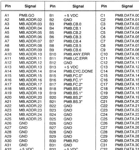
1. Plug one - Connects to the ICB. Contains power supply voltages, 16 ICB data lines, a total of ICB address and strobe lines that allows up to 24 bits of address, various system voltages and grounds, the processor clock signal, 3 unused/reserved lines, 7 interrupt request lines, a system reset line, and an ICB bus error line.
2. Plug two - Utitility control bus. Contains power supply voltages and status, timing, PMB request and grant signals, power supply control signals, and slot address identification signals.
3. Plug three - Connects to the PMB. Contains power supply voltages, all PMB address and data lines, and related PMB status and control data lines.
4. Jack four - Output connector to the system console terminal.
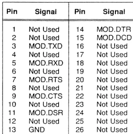
5. Jack Five - Output connector to a modem. Identical to Plug four, but provides for a remote terminal to be the system console terminal via the modem connection.
Plug One
This connector (Figure 5-1) contains a total of 96 conductors. It connects to the ICB on the backplane. The +5 vdc supply voltage comes in on 11 pins; the -12 vdc supply voltage comes in on 1 pin; and the
+
12 vdc comes in on 1 pin. The data word for the ICB is 16 bits wide, and comes in on 16 pins. The clock signal is the processor clock, which is not used on this board. The upper and lower data strobe signals are derived from the size, data strobe and the low-order address of the MC68020. The UOS and LOS is effectively the first of 24 ICB address bits.•
Interface Description
Section 5
There are 3 pins designated as "not used." These pins, however, are reserved for future use, and are not available. There are 7 interrupt request lines. Each line is open-collector and driven from a decoder. Interrupt requests are not acknowledged. An active interrupt request generates an appropriate auto vector on the master CPU. All interrupts are handled by the master CPU. Interrupts are cleared during the routine that services the interrupt. The master CPU clears the request at the slave CPU or DMC where it originated. Requests 1 through 4 are from the slave CPUs, and request 5 is from the DMC.
Level Mode Remarks
7 Autovector Power fail
6 Autovector Timer
5 Autovector ICB Interrupt Request Five
4 Autovector Serial Port or ICB Interrupt Request Four
3 Autovector ICB Request
2 Autovector ICB Request
1 Autovector ICB Request
The ICB bus error signal is asserted by the HSDT if it has a fault and the CPU select it. The system reset signal comes from the power up signal or from a CPU reset instruction on the master CPU. System reset does not reset the master CPU, but it does reset all the other boards in the system.
•
Section 5
Iriterface Description
Pin Signal Pin Signal Pin Signal A1 ICB.DATA.OO B1 Not Used C1 ICB.DATA.08 A2 ICB.DATA.01 B2 Not Used C2 ICB.DATA.09 A3 ICB.DATA.02 B3 Not Used C3 ICB.DATA.10 A4 ICB.DATA.03 B4 GND C4 ICB.DAT A.11 AS ICB.DATA.04 BS GND CS ICB.DATA.12 A6 ICB.DATA.OS B6 GND C6 ICB.DATA.13 A7 ICB.DATA.06 B7 GND C7 ICB.DATA.14 A8 ICB.DATA.07 B8 GND C8 ICB.DATA.1S A9 GND B9 GND C9 GND
A10 ICB.CLK B10 GND C10 GND
[image:46.618.96.511.130.613.2]A11 GND B11 GND C11 ICB.BERR* A12 ICB.UDS* B12 +5 VDC C12 SYS.RESET* A13 ICB.LDS* B13 +5 VDC C13 +5 VDC A14 ICB.RD B14 +5 VDC C14 +5 VDC A1S GND B1S +5 VDC C1S ICB.ADDR.23 A16 ICB.DTACK'" B16 GND C16 ICB.ADDR.22 A17 GND B17 GND C17 ICB.ADDR.21 A18 ICB.AS* B18 GND C18 ICB.ADDR.20 A19 GND B19 GND C19 ICB.ADDR.19 A20 GND B20 GND C20 ICB.ADDR.18 A21 GND B21 GND C21 ICB.ADDR. 17 A22 GND B22 GND C22 ICB.ADDR.16 A23 +5 VDC B23 GND C23 ICB.ADDR.1S A24 ICB.ADDR.07 B24 ICB.lRQ.7* C24 ICB.ADDR.14 A2S ICB.ADDR.06 B2S ICB.IRQ.6'" C2S ICB.ADDR.13 A26 ICB.ADDR.OS B26 ICB.IRQ.S'" C26 ICB.ADDR.12 A27 ICB.ADDR.04 B27 ICB.IRQ.4* C27 ICB.ADDR.11 A28 ICB.ADDR.03 B28 ICB.IRQ.3* C28 ICB.ADDR. 1 0 A29 ICB.ADDR.02 B29 ICB.IRQ.2* C29 ICB.ADDR.09 A30 ICB.ADDR.01 B30 ICB.lRQ.1'" C30 ICB.ADDR.08 A31 -12 VDC B31 +5 VDC C31 +12 VDC A32 +5 VDC B32 +5 VDC C32 +5 VDC
Figure 5-1. Plug One