Abstract-- This paper presents a hybrid Modular Multilevel Converter (MMC), which combines full-bridge sub-modules (FBSM) and half-bridge sub-modules (HBSM). Compared with the FBSM based MMC, the proposed topology has the same dc fault blocking capability but uses fewer power devices hence has lower power losses. To increase power transmission capability of the proposed hybrid MMC, negative voltage states of the FBSMs are adopted to extend the output voltage range. The optimal ratio of FBSMs and HBSMs, and the number of FBSMs generating a negative voltage state are calculated to ensure successful dc fault blocking and capacitor voltage balancing. Equivalent circuits of each arm consisting of two individual voltage sources are proposed and two-stage selecting and sorting algorithms for ensuring capacitor voltage balancing are developed. Comparative studies for different circuit configurations show excellent performance balance for the proposed hybrid MMC, when considering dc fault blocking capability, power losses, and device utilization. Experimental results during normal operation and dc fault conditions demonstrate feasibility and validity the proposed hybrid MMC.
Index Terms-- DC fault, hybrid, modular multilevel converter, power losses, voltage ripple.
I. INTRODUCTION
The Modular Multilevel Converter (MMC) has drawn attention due to its advantages of modular design, high efficiency and scalability, and excellent output waveform with low harmonic distortion, etc. [1-12].
The basic building block in a MMC is a sub-module (SM). The half-bridge based SM (HBSM) has been the main configuration in the MMC [1-7]. However, a HBSM based MMC (HB-MMC) does not have dc fault blocking capability, thus relies on ac or dc circuit breakers to isolate dc faults [13-14]. This becomes problematic for both the converter as it has to withstand a high fault current and the connected network since it could take considerable time for the system (especially a multi-terminal system) to recover a dc fault [15]. Thyristors connected in anti-parallel to the SM terminals can be employed [16-17] to bypass the short-circuit current and protect the freewheel diodes. However, this method does not isolate a dc fault and additional devices are required for fast fault isolation.
To address the issues of dc faults, the full-bridge based SM
R. Zeng, L. Xu and B.W. Williams are with Department of Electronic and Electrical Engineering, University of Strathclyde, Glasgow G1 1XW, UK (email: [email protected], [email protected],
L.Z. Yao is with China Electric Power Research Institute, Xiaoying Road, Beijing, 100192, China (email: [email protected])
(FBSM) was proposed which has the inherent advantage of dc fault blocking capability. However, the number of SM power devices is doubled compared to the HBSM. This not only increases the costs of high power MMC systems but also results in higher power loss as the current in each SM flows thought two power devices instead of one as in a HBSM. To increase power device utilization, various studies have been performed which use the negative voltage output from the FBSM to increase the modulation index and ac voltage output [8-10]. In [8] the concept of using the negative voltage state of the FBSM to increase voltage output was mentioned, but no detailed relationship between the ac and dc voltages and modulation index limit were considered. The relationship among the capacitor voltages, the ac and dc voltages was presented in [9], but the effect of the use of a negative voltage state on energy variation and capacitor voltage ripple are not addressed. In [10], the focus was on eliminating the energy oscillation between the upper and lower arms using a desirable modulation index of 1.414 for a full-bridge based MMC (FB-MMC). However, for all studies that consider the use of the FBSM negative voltage state, no systematic design and detailed analysis on SM capacitor voltage variation, has been provided.
Voltage ripple and capacitance of the SM capacitors are a crucial factor for the operation, size and cost of MMC systems [18-23]. For HB-MMC systems, a method to calculate the capacitance was derived in [18], considering the energy variation and the corresponding voltage ripple. The minimum capacitance in terms of voltage balancing requirements has been investigated in [19]. A method to minimize the required capacitance by injecting harmonics into the circulating current was proposed in [20]. The minimum capacitance and the energy storage requirements with respect to the energy variation were analyzed in [21] and [22], respectively. A detailed analysis on the impact of the circulating current on capacitor voltage ripple is provided in [23]. For a FB-MMC using the negative voltage state, the effect of the number of FBSMs allowed to generate the negative voltage state, on capacitor voltage balancing, has not been investigated.
Reference [24] illustrates how HBSM can be used as the basic building blocks to form different circuit configurations by varying the connections of the respective output terminals in order to provide a space-saving, simple structure, easy to maintain, durable and cost-effective power electronic switching module. For example, a FBSM can be implemented by parallel connection of the dc sides and series connection of the ac sides of two HBSMs, and further parallel and series connection of the ac/dc sides can be made to form different circuit configurations. However, there is no mention of the use
Design and Operation of a
Hybrid Modular Multilevel Converter
of different configurations within the same converter leg. Considering the mentioned issues, a Hybrid MMC consisting of a combination of FBSMs and HBSMs, is proposed in this paper. The hybrid MMC not only has dc fault blocking capability but also uses fewer semiconductor devices and has lower power loss than the FB-MMC. However, in contrast to the conventional MMC in which all the SMs are identical, FBSMs and HBSMs in the Hybrid MMC function differently in the charging and discharging periods and therefore, their capacitor voltage ripple and balancing need to be carefully analyzed.
The paper is organized as follows. Section II introduces the basic topology and design principles of the proposed Hybrid MMC. The detailed analysis of capacitor voltage ripple and the proposed SM sorting and selecting algorithm are discussed in Section III. Comparison among the different MMC topologies is carried out in Section IV. Section V provides the experimental results to demonstrate the feasibility of the proposal and Section VI draws the conclusions.
II. HYBRID MMCDESIGN PRINCIPLE
A. Basic Configuration
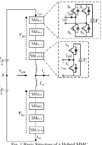
Fig. 1 shows one leg of the proposed Hybrid MMC. Each of the two arms in each leg has N sub-modules, comprising F
FBSMs, notated as SMf(1) to SMf(F) and N-F HBSMs denoted as SMh(1) to SMh(N-F). Vdc is the dc-link voltage, L0 is the arm
inductance, C is the SM capacitance, and Vc is the dc voltage
across each SM capacitor. The total voltages generated by all the SMs in the upper and lower arms are represented by vpa
and vna, respectively. ipa and ina are the upper and lower arm
[image:2.612.89.264.433.682.2]currents, respectively, and ia is the output ac phase current.
Fig. 1 Basic Structure of a Hybrid MMC
Tables I and II show the switch states for an FBSM and HBSM, respectively. Compared to the HBSM which can generate voltage states Vc and 0, each FBSM can generate a
third state of -Vc. In the proposed scheme, some of the FBSMs
are allowed to generate the -Vc voltage state to increase the ac
output voltage.
TABLEI SWITCH STATES OF FBSM
STATE S1 S2 S3 S4 vsm Vc (isM>0)
1 1 0 0 1 VC charging
2 0 1 0 1 0 unchanged
3 1 0 1 0 0 unchanged
4 0 1 1 0 -VC discharging
BLOCK 0 0 0 0 - -
TABLEII SWITCH STATES OF HBSM
STATE S1 S2 vsm Vc (isM>0)
1 1 0 VC charging
2 0 1 0 unchanged
Assuming the total number of SMs in each arm is N
(comprising F FBSMs and N-F HBSMs) and the capacitor voltage across all the SMs are balanced at Vc, the range of the
generated total arm voltage is from 0 to NVc for the conventional method without using the -Vc state of the FBSMs.
Thus, considering a maximum modulation index m of 1, the dc and peak ac phase voltages are:
dc c peak an c
dc NV V NV V
V , _ 12 12 (1) If M FBSMs in the Hybrid MMC are allowed to generate the -Vc state in each arm (M < F), the arm voltage range will be
extended, between –MVc and NVc. Under such conditions, the
dc and peak ac phase voltages are:
M N
MV V V M N V
V M N V
dc dc c peak
an
c dc
2 1 2
1 _
(2)
From (2) the peak ac phase voltage can be extended due to
M FBSMs generating the -Vc state.
B. Capacitor voltage balancing consideration
For satisfactory MMC operation it is necessary to ensure the capacitor voltage in each SM can be balanced. In contrast to FBSMs that can charge and discharge their SM capacitors without having to change the external current direction, HBSM capacitors can only be charged during positive arm current and discharged during negative arm current. As the number of FBSMs generating a -Vc state increases, the relationships
among the ac voltage, dc voltage, and dc current also change. Thus it is necessary to analyze the impact of the number of FBSMs generating the -Vc state on the charging and
discharging time for the SM capacitors.
Neglecting converter power loss, the steady-state three-phase ac and dc powers are:
ac m
m dc dc
dc V I V I P
P 32 cos (3) where Vm and Im are the peak ac output phase voltage and
current, φ is the voltage and current phase angle, and Idc is the
dc current.
Substituting Vm12mVdc into (3) yield
cos 4
3 m
dc mI
I (4)
Considering the fundamental frequency and dc components, the arm currents are given by
dc m n dc m p I t I i I t I i 3 1 sin 2 1 3 1 sin 2 1 (5)Substituting (4) into (5) yields
cos 4 1 sin 2 1 cos 4 1 sin 2 1 m m n m m p mI t I i mI t I i (6)To ensure sufficient charging and discharging times for the HBSMs, the arm currents must be both positive and negative within one complete period. So the following equation must be satisfied:
m m
m mI I
mI cos 14 12 4
1 (7) Thus the modulation index m must be less than or equal to 2. According to (2), the following relationship can be derived:
V M N
M N
MV
Vdc dc dc, 13 2
1
(8)
It can be concluded that for the Hybrid MMC, M (the number of FBSMs generating -Vc) must not be more than ⅓N
in order to ensure sufficient charging and discharging times for the HBSMs to balance their capacitor voltages within each fundamental period.
C. DC fault blocking consideration
If the series voltage formed by all the FBSM capacitors along a fault current path is higher than the ac line-to-line voltage, a dc fault can be blocked once all the IGBTs are switched off. In view of this requirement, the minimum number of FBSMs within each arm can be derived.
According to (2), the peak line-to-line ac voltage for the MMC during a dc fault, at maximum modulation index, is
NN MM
Vdcu 2 3
max (9)
Each arm has F FBSMs, thus the arm voltage formed by the FBSMs during dc faults is
dcc
arm FV NFM V
u
(10)
Therefore, the blocking voltage formed by two series arm voltages (one upper arm and one lower arm in different legs) and the ac line-to-line voltage should meet the following criteria
NN MM
Vdc
N FM
Vdc uarmu 2 2
2 3
max (11)
Thus, to successfully block dc faults, the total number of FBSMs has to meet the following requirement
N M
F
4
3 (12) According to this analysis, both (8) and (12) need be satisfied when designing the hybrid MMC. Fig. 2 (a) shows the minimum allowed F/N value, which results in the lowest number of required power device, for the variation of M/N
from 0 to 1/3. In Fig. 2 (b), the normalized maximum IGBT utilization where the value at M = 0 is defined as 1 (higher value means better use of the IGBT or for delivering same power, less IGBT would be required), is illustrated. As can be seen, the maximum device utilization increases with the increase of the M/N value.
M/N F /N M/N IG B T u ti li za ti on
[image:3.612.317.554.61.138.2](a) (b)
Fig. 2 Impact of M variation on F value and IGBT device utilization Two specific conditions are considered further as examples for analyzing the circuit and control strategy.
1) M = 0, F = ½N
In this scenario, the hybrid MMC consists of half HBSMs and half FBSMs. Since M=0, there is no -Vc state used for the
FBSMs, the number of HBSMs and FBSMs are same (½N) and the conventional control strategy for the HB-MMC [2] can be adopted. No further discussion is presented here.
2) M = ⅓N, F = ⅔N
In this scenario, the hybrid MMC consists of ⅓N HBSMs and ⅔N FBSMs (i.e., F=⅔N). Among the ⅔N FBSMs, the maximum number of SM generating -Vc state is half of the
total FBSMs, i.e., ⅓ of the total number of SMs (M=⅓N). This configuration is now investigated further.
III. CAPACITOR VOLTAGE BALANCING
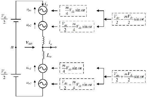
Due to the use of the negative voltage state for some SMs, the total voltage in each arm can be considered as two series-connected voltage sources as shown in Fig. 3. As shown, up1
and un1 refer to the ac voltages having amplitudes of ¼mVdc
generated by the M (i.e., ⅓N) FBSMs utilizing the -Vc state. up2 and un2 are the voltages generated by the remaining N-M
SMs with the same ac voltage amplitudes of ¼mVdc but with a
dc offset of ½Vdc.
Fig. 3 Equivalent circuit for the Hybrid MMC
A. Steady-state analysis
Since the analysis in the upper and the lower arms in a leg is the same, the following analysis is based on the upper arm.
According to the presented analysis, the total arm voltage can be divided into two parts
t mV V u t mV u dc dc p dc p sin 4 1 2 1 sin 4 1 2 1 (13)
[image:3.612.317.561.448.609.2]
t I mV I mV t I V m mI t I t mV i u p m dc m dc m dc m m dc p p p 2 cos 16 cos 16 sin cos 16 cos 4 sin 2 sin 4 2 1 1 (14)
t I mV I mV t I V m t I V mI t I t mV V i u p m dc m dc m dc m dc m m dc dc p p p 2 cos 16 cos 16 sin cos 16 sin 4 cos 4 sin 2 sin 4 2 2 2 2 (15)Integrating the instantaneous power in one fundamental period yields the net energy flowing into each voltage source as 0 cos 8 1 2 0 1
1
Ep
ppdt mVdcIm (16)0 cos 8 1 2 0 2
2
Ep
pp dt mVdcIm (17)0 2 1
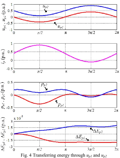
E Ep Ep (18) From (18), although the net energy transferring in one fundamental period in each arm is zero, the net energy in the two separate up1 and up2 is not zero. Therefore, in order to
maintain capacitor voltage balance, it is necessary to exchange energy between up1 and up2 within each fundamental period.
For this hybrid MMC configuration, ⅓N FBSMs are operated in up1, and the other ⅓N FBSMs are operated in up2. Thus, if each FBSM can be arranged to operate in both up1 and up2 by
[image:4.612.70.304.51.179.2]specific sorting and selecting algorithms, they can be used as a bridge for transferring energy between up1 and up2.
Fig. 4 Transferring energy through up1 and up2
B. Modified sorting and selection algorithm
As indicated in (6), increasing m in the proposed hybrid MMC gradually reduces the time intervals when the upper arm current ip is negative. This affects capacitor voltage balance in
the HBSMs due to the reduced discharging time. Thus, in contrast to the conventional capacitor voltage balancing algorithm [2], in which only capacitor voltage and arm current direction are used for SM selection, the selection of SMs in the hybrid MMC has to consider the differences in their behavior, and charging and discharging periods between the FBSMs and HBSMs.
For illustrative purposes, Fig. 4 shows the reference voltages, arm current, and transferred energy in up1 and up2 in
one complete period for φ = 0. From Fig. 4, ΔEp1 and ΔEp2
cannot reach balance in one complete period, as previously illustrated in (16) and (17). In the first half-cycle (0 to π), up1
delivers energy while up2 absorbs energy. Thus it is necessary
to transfer energy between these two voltage sources to ensure their respective net energy flow can remain balanced in one complete period. A modified sorting and selecting algorithm is thus proposed, as shown in Fig. 5.
Fig. 5 Modified sorting and selection algorithm for the hybrid MMC The basic principles of the modified sorting and selection algorithm are summarized as follows.
In the first half-cycle period (0 to π), all ⅔N FBSMs are sufficient to generate the required reference voltages in up1
and up2 (within 0 - ±0.5 p.u.). Thus only the ⅔N FBSMs
are sorted and selected in this period with all the HBSMs producing zero output (i.e., their capacitors are bypassed). When the arm current is positive, the FBSMs having the highest capacitor voltages are selected to operate in up1
producing -Vc output and their capacitors are discharged.
The FBSMs having the lowest capacitor voltages are assigned to up2 producing +Vc output and their capacitors
[image:4.612.70.277.410.682.2] In the second half-cycle period (π to 2π), no -Vc state is
required. The sorting process is thus carried out within all
N SMs where the SMs with the lowest capacitor voltages (for positive arm current) or the highest capacitor voltages (for negative arm current) are selected to operate in up1 and up2 producing +Vc output. All the unselected SMs are
bypassed generating zero voltage.
As the FBSMs are switched between up1 and up2 which
effectively transfers energy between the two equivalent sources, all the capacitor voltages can be balanced.
C. Variations on capacitor energy storage
Due to the interactive behavior between the FBSMs and HBSMs, their capacitor voltage ripple is now considered.
For the example in Fig. 4, the maximum discharging energy variation on the FBSM capacitors occurs in the first half-cycle, and can be expressed as
1 0 20 1 2
2 1 max 2 cos 8 1 sin cos 8 1 sin 4 1 max max dt t I mV t I V m t I V dt p p dt p p E m dc m dc m dc p p p p fd (19)
where θ1 refers to the phase angle resulting in maximum
discharging energy variation.
The charging energy variation on capacitors in the FBSMs occurs in the second half-cycle before the arm current is negative. Initially, the FBSMs are selected to be charged so as to compensate the discharged energy in the first half-cycle. After compensation is completed, the following charge energy is then assumed to be equally distributed among the ⅔N
FBSMs and ⅓N HBSMs groups. So the maximum charging energy variation in the FBSM capacitors is
2
0 1 2
max 23
dt p p
Efc p p (20)
where θ2 is the phase angle when the arm current becomes
negative.
Thus, the maximum energy variation on the FBSM capacitors is calculated as
max max
max fc fd
f E E
E
(21)
For the HBSMs, the total energy flowing in the whole second half-cycle is zero for the capacitor voltages to be balanced. Since HBSMs can be discharged only when iarm< 0,
if the discharge energy is assumed to be equally distributed among the ⅔N FBSM and ⅓N HBSM groups, the maximum energy variation on the HBSM capacitors can be estimated by considering one third of the total discharging energy when iarm
< 0, i.e.:
3 2 2 1 max 13
p p dt
Eh p p (22)
where θ2 to θ3 is the period when the arm current is negative.
According toEmaxEmaxEmin, the maximum energy variation can also be estimated:
fc fc
dc
f
f
ff f C M N F D D V F u u C E 2 2 min 2 max 2 2 min 2 max max 2 2
(23)
h
hh dc hc hc h h C M N F N D D V F N u u C E 2 2 min 2 max 2 2 min 2 max max 2 2 1 (24)
where Dfmax, Dhmax and Dfmin, Dhmin denote the per unit
maximum and minimum capacitor voltage for the FBSMs and HBSMs, respectively.
Substituting (21) and (22) into (23) and (24), the capacitance for the FBSMs and HBSMs can be expressed as
2
maxmin 2 max 2 2 2 f f f dc f E F D D V M N
C
(25)
2
maxmin 2 max 2 2 2 h h h dc h E F N D D V M N C
(26)
The required capacitances for the HBSMs and FBSMs are different for the same voltage ripple and are also affected by operating conditions (i.e., ΔEfmax and ΔEhmax vary under
different operation conditions). Taking the experimental prototype for example, when the capacitance ratio of the FBSM and HBSM is 4.46:1, the maximum capacitor voltage ripples are equal (N = 3, F = 2, M = 1, m = 1.6, Vdc = 120V, Im
= 7A, φ = 0).
D. Operation under reduced dc voltage
The above analysis is based on the normal operation with DC voltage controlled under nominal values. However, large disturbances, e.g., faults on ac or dc side can cause severe dc voltage drop. Under such a condition, conventional HB-MMC based system would lose its control capability and have to be blocked to protect the IGBTs. With the proposed hybrid configuration, the relationship between the ac and dc voltages can be altered by changing the total number of SMs switched in (i.e. N) and the number of FBSMs generating -Vc state (i.e., M). However, the capacitor voltage balance in the FBSMs and HBSMs needs be considered carefully.
The total number of required SMs selected is now N’ and the number of FBSMs generating the –Vc state is M’.
Assuming the ac system voltage remains the same whereas the dc voltage has dropped from Vdc to Vdc’, the dc and ac phase
voltages can be expressed as,
c
cdc
dc kV k N MV N M V
V' ' ' (27)
c
cm N MV N M V
V ' '
2 1 2 1
(28)
where k is the ratio between the new and initial dc voltages, and k < 1.
According to (27) and (28), the N’ and M’ are then calculated as,
M k N k M M N k M k N N 1 2 1 2 1 2 1 2 ' ' (29)It is noted that the N’ will have to decrease and M’ to increase following the drop of dc voltage. Under the extreme condition of V’dc = 0 (i.e. k = 0), M’ = N’ = (M+N)/2. For
dc voltage conditions, the HBSMs will still be used. The power on ac and dc sides are given as,
' ' ' '
'
' cos
2 3
ac m
m dc dc
dc V I V I P
P (30)
where I’dc is the new dc current, I’m and φ’ are the new ac
current amplitude and power factor angle, respectively. The upper arm current is now rewritten as,
dcm
p I t I
i' ' ' '
3 1 sin
2 1
(31)
Substituting (30) into (31) yields,
dcdc m
dc
p VV I t I
i ' ' '
' '
3 1 sin
cos
3
(32)
To ensure sufficient charging and discharging times for the HBSMs, the arm currents must be both positive and negative within one complete period. So the following equation must be satisfied:
dc dc m
dc I I
V
V' ' '
3 1 cos
3 (33) Substituting (27) and (28) into (33) gives the required power factor as
N M
M N k
2
cos' (34)
Equation (33) indicates that the power factor should be reduced following the drop of dc voltage. That means the control system needs use reactive current to ensure enough discharging period for HBSMs so as to maintain SM capacitor voltage balancing. Again for the proposed design of M=⅓N, this leads to cos'k (k<1).
Thus, the proposed hybrid MMC can continue operating under reduced dc voltage with proper selection of the total number of SMs to be used (i.e., N’), the number of FBSMs generating –Vc (i.e., M’), and the output power factor (i.e., φ’).
The previously proposed sorting and selection algorithm is still applicable for maintaining SM capacitor voltage balancing and the system simply operates in the same way as normal condition, e.g. controlling the AC output and circulating current. The maximum energy variations on FBSMs and HBSMs can still be derived from (23) and (24) by replacing N,
M, φ with N’, M’ and φ’ from (29) and (34), and the SM capacitor voltage ripple can be estimated accordingly.
IV. TOPOLOGY COMPARISON
A comparison among the hybrid MMC systems and the conventional HB-MMC and FB-MMC is carried out. Since the basic building blocks in the hybrid MMC are the same HBSM and FBSM as the conventional MMC, the reliability of the hybrid MMC would be similar to the HB-MMC and FB-MMC.
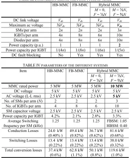
Table III shows the number of power semiconductors required for the different types of MMC. Taking the required semiconductor devices for the conventional HB-MMC as the bases for comparison, in which 4n IGBT and 4n diode are required for each arm, for delivering the same power, the conventional FB-MMC doubles the number of IGBT and diode (i.e., 8n ), whereas the proposed hybrid MMC (M = 0, F
= ½N) uses 50% more IGBT and diode (i.e., 6n) and the hybrid MMC (M = ⅓N, F = ⅔N) only has 25% increase in the
total number of IGBT and diode (i.e., 5n) compared to HB-MMC. This indicates that the proposed hybrid MMC system can provide dc fault blocking capability without significant increase on the total semiconductor devices.
To evaluate the power losses of the four MMC configurations, a simple loss calculation method is adopted [5]. The main parameters of the semiconductor module are derived from the datasheet of the 5SNA 1200G450300 [25], and the main parameters of the four MMC systems are shown in Table IV. The carrier frequency is 2.5 kHz for all four MMCs and the actual switching frequency for the SMs are also shown in Table IV.
TABLE IIICOMPARISON AMONG THE FOUR TYPES OF MMC HB-MMC FB-MMC Hybrid MMC
M = 0, F = ½N
M = ⅓N, F = ⅔N DC link voltage Vdc Vdc Vdc Vdc
Maximum ac voltage ½Vdc ½Vdc ½Vdc Vdc
SMs/per arm 2n 2n 2n 3n
IGBTs/per arm 4n 8n 6n 10n
Diodes/per arm 4n 8n 6n 10n
Power capacity (p.u.) 1 1 1 2
Power capacity per IGBT 1/(4n) 1/(8n) 1/(6n) 1/(5n) DC fault blocking No Yes Yes Yes
TABLEIV PARAMETERS OF THE DIFFERENT SYSTEMS
Item HB-MMC FB-MMC Hybrid MMC
M = 0, F = ½N
M = ⅓N, F = ⅔N MMC rated power 5 MW 5 MW 5 MW 10 MW
DC voltage 5 kV 5 kV 5 kV 5 kV
AC voltage (L-L rms) 2.5 kV 2.5 kV 2.5 kV 5 kV
No. of SMs per arm (N) 2 2 2 3
No. of IGBTs per arm 4 8 6 10
SM capacitor voltage 2.5 kV 2.5 kV 2.5 kV 2.5 kV Power capacity per IGBT 4.2% 2.1% 2.8% 3.3%
Average Switching frequency per SM (kHz)
1.25 1.25 1.25 FBSM: 1.05 HBSM: 0.40 Conduction Losses 24.0 kW
(0.40% )
49.4 kW (0.82%)
36.7 kW (0.62%)
81.6 kW (0.68%) Switching Losses 13.4 kW
(0.22%)
13.4 kW (0.22%)
13.4 kW (0.22%)
38.0 kW (0.32%) Total conversion losses 37.4 kW
(0.6%)
62.8 kW (1.1%)
50.1 kW (0.8%)
119.6 kW (1.0%) The conduction losses and switching losses of the four MMC systems are also shown in Table IV. As expected, the conventional HB-MMC is the most efficient among the four MMC types. The proposed Hybrid MMCs are shown as more efficient than the conventional FB-MMC due to the reduced switch number, hence conduction loss. The two hybrid configurations also have different features; M = ⅓N, F = ⅔N
results in a higher power density but slightly higher power loss than the configuration of M = 0, F = ½N, since the former needs extra switching for capacitor voltage balancing.
V. EXPERIMENTAL RESULTS
To verify the presented analysis for the Hybrid MMC with
[image:6.612.307.568.205.521.2]main parameters are listed in Table V. Two series-connected large DC capacitors are parallel connected across the DC power supply to create the neutral point.
[image:7.612.58.296.265.632.2]Figs. 7 and 8 respective show the steady-state and dynamic performances of the proposed hybrid MMC operating as an inverter in grid-connected mode, i.e. active power flows from the dc to ac. The output current shown in Fig. 7 is almost sinusoidal with low distortion. Voltage ripple on the FBSM capacitors is generally the same, with a peak-to-peak ripple of 11.7%. Maximum voltage ripple on the HBSM capacitors is about 2.7%, being lower than that of the FBSMs due to the same capacitance being used (940µF). These values are in agreement with the calculated ripple of 11.99% and 2.69% using (23) and (24) for the FBSMs and HBSMs, respectively. The HBSM is bypassed during the first half-cycle period, verifying the previous sorting analysis. All capacitor voltages remain balanced. In Fig. 8, the active power is stepped from 220W to 400W at 75ms. The proposed Hybrid MMC tracks the current and power changes quickly and smoothly, and the capacitor voltages remain balanced during the transient. The FBSM capacitor voltage ripple is considerably larger after the power step (current increase) due to increased ΔEfmax.
Fig. 6 Schematic diagram of the experimental system TABLEV
PARAMETERS OF THE EXPERIMENTAL MMCSYSTEM
Item Values
MMC rated power 400 W
dc voltage 120 V
ac voltage (phase-ground rms.) 72 V Number of SMs per arm 3 Number of FBSMs per arm 2 Number of HBSMs per arm 1
DC voltage per SM 60 V
SM capacitor 940 µF
Inductance per arm 5 mH MMC switching frequency 2.5 kHz
To further validate the relation between voltage ripple and capacitance, Fig. 9 shows the measured voltage ripple for different capacitances. In these tests, the FBSM capacitance is fixed at 940µF, while capacitance for the HBSMs is varied at 940µF, 470µF and 235µF, respectively. As shown in Fig. 9, for the same capacitance, the maximum voltage ripples in the FBSMs and HBSMs with 940µF are approximately 11.7% and 2.7%, respectively. The respective maximum voltage ripple in
the HBSM rises to 6.7% with 470µF and 10.0% with 235µF. These values are in agreement with the calculated HBSM capacitor voltage ripples of 2.69%, 5.37% and 10.75% for 940µF, 470µF and 230µF, respectively.
Fig. 10 shows the experimental results during a dc line-to-line fault applied on the hybrid MMC system. Initially, the hybrid MMC operates as a rectifier, absorbing active power (-245W) from the ac grid into the dc side (S1 is open). A dc fault is emulated by connecting a 2Ω resistor across the dc link (S2 is closed). Immediately after the fault, the MMC remains operational until it is blocked when the over-current is detected as shown in Fig. 10 where iarm increases rapidly after
the dc fault. The capacitors in the selected SMs discharge before converter blocking. The dc voltage collapses quickly. Once the IGBTs are gated off, the fault current flows through the series capacitors in the FBSMs, while the capacitor in the HBSM is bypassed. There is a short charging period for the FBSM capacitors, whereas the HBSM capacitor voltage remains constant after IGBT blocking. Since the total series voltage formed by the FBSMs is higher than the ac voltage, the ac current and arm current quickly reduce to zero and the dc fault is thus blocked.
Fig. 7 Steady-state operation as an inverter, Vdc: dc voltage (120V/div); vg:
grid voltage (170V/div); ig: grid current (12A/div); iarm: arm current (6A/div);
vcf1: capacitor voltage in FBSM1 (10V/div); vcf2: capacitor voltage in FBSM2
[image:7.612.321.555.313.678.2] [image:7.612.56.296.323.472.2]Fig. 8 Dynamic operation as an inverter during active power step, Vdc: dc
voltage (120V/div); vg: grid voltage (170V/div); ig: grid current (6A/div); iarm:
arm current (6A/div); vcf1: capacitor voltage in FBSM1 (10V/div); vcf2:
capacitor voltage in FBSM2 (10V/div); vch: capacitor voltage in HBSM
(10V/div)
Fig. 9 Relation between capacitor ripple and capacitor value, vcf1: capacitor
voltage in FBSM1 (10V/div); vcf2: capacitor voltage in FBSM2 (10V/div); vch:
[image:8.612.324.555.46.425.2]capacitor voltage in HBSM (10V/div)
Fig. 10 DC fault, Vdc: dc voltage (120V/div); vg: grid voltage (170V/div); ig:
grid current (12A/div); iarm: arm current (6A/div); vcf1: capacitor voltage in
FBSM1 (20V/div); vcf2: capacitor voltage in FBSM2 (20V/div); vch: capacitor voltage in HBSM (20V/div)
[image:8.612.60.291.46.414.2] [image:8.612.57.292.484.669.2]Fig. 11 DC voltage drop, vdc: dc voltage (120V/div); vg: grid voltage
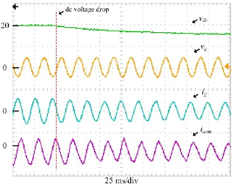
(170V/div); ig: grid current (12A/div); iarm: arm current (6A/div)
VI. CONCLUSION
This paper proposes a hybrid MMC configuration consisting of FBSMs and HBSMs. By adopting the negative voltage state for some of the FBSMs, the output voltage range is extended to increase converter power transmission capability. By considering the relationships between the ac and dc voltages, ac, dc and arm currents, the ratio of FBSM to HBSM were analyzed in order to maintain capacitor voltage balance and retain dc fault blocking capability. An equivalent circuit for the hybrid MMC is proposed, which considers each arm to be consisted of two individual voltage sources. This model is used to analyze SM capacitor voltage balancing and ripple. A two-stage selection and sorting algorithm is developed to ensure capacitor voltage balancing among the SMs. The proposed Hybrid MMC is compared to other topologies in terms of power device utilization and power losses. This comparison shows that the Hybrid MMC has higher device utilization and lower power loss than the conventional FB-MMC. Experiment results during steady state, power step and dc fault verify the theoretical analysis. The proposed hybrid MMC is a possibility for high power transmission application where dc fault blocking capability is required.
VII. REFERENCES
[1] A. Lesnicar and R. Marquardt, “An innovative modular multilevel converter topology suitable for a wide power range,” in Proc. IEEE Bologna Power Tech. Conf., Jun. 2003, vol. 3, pp. 1-6.
[2] M. Saeedifard and R. Iravani, “Dynamic performance of a modular multilevel back-to-back HVDC system,” IEEE Trans. Power Del., vol. 25, no. 4, pp. 2903-2912, Oct. 2010.
[3] L. Harnefors, A. Antonopoulos, S. Norrga, L. Angquist and H. -P. Nee, “Dynamic analysis of modular multilevel converters,” IEEE Trans. Ind. Electron., vol. 60, no. 7, pp. 2526-2537, Jan. 2013.
[4] Q. R. Tu, Z. Xu and L. Xu, “Reduced switching-frequency modulation and circulating current suppression for modular multilevel converters,” IEEE Trans. Power Del., vol. 26, no. 3, pp. 2009-2017, Jul. 2011. [5] S. Rohner, S. Bernet, M. Hiller and R. Sommer, “Modulation, losses,
and semiconductor requirements of modular multilevel converters,” IEEE Trans. Ind. Electron., vol. 57, no. 8, pp. 2633-2642, Aug. 2010. [6] K. Ilves, A. Antonopoulos, S. Norrga and H. Nee, “Steady-state analysis
of interaction between harmonic components of arm and line quantities
of modular multilevel converters,” IEEE Trans. Power Electron., vol. 27, no. 1, pp. 57-68, Jan. 2012.
[7] G. Mondal, R. Critchley, F. Hassan and W. Crookes, “Design and simulation of a modular multi-level converter for MVDC application,” in Proc. IEEE Int. Symp. Ind. Electron., Jun. 2011, pp. 200-205. [8] L. Baruschka, A. Mertens., “Comparison of Cascaded H-Bridge and
Modular Multilevel Converters for BESS application,” in Proc. Energy Conv. Cong. and Expo. (ECCE), Sept. 2011, pp. 909-916.
[9] N. Thitichaiworakorn, M. Hagiwara and H. Akagi, “Experimental verification of a modular multilevel cascade inverter based on double-star bridge-cells (MMCI-DSBC),” in Proc. Energy Conv. Cong. and Expo. (ECCE), Sept. 2012, pp. 4196-4202.
[10] K. Llves, S. Norrga and H.-P. Nee, “On energy variations in modular multilevel converters with full-bridge submodules for Ac-Dc and Ac-Ac applications,” in Proc. Power Electron. and Appl. (EPE), Sept. 2013, pp. 1-10.
[11] R. Marquardt, "Modular Multilevel Converter topologies with DC-Short circuit current limitation," in Proc. IEEE Power Electron. and ECCE Asia, May, 2011, pp. 1425-1431.
[12] R. Marquardt, “Modular Multilevel Converter: An universal concept for HVDC-Networks and extended DC-Bus-applications,” in Proc. Int. Power Electron. Conf., Jun. 2010, pp. 502-507.
[13] L. X. Tang and B. –T. Ooi, “Locating and isolating DC faults in multi-terminal DC systems,” IEEE Trans. Power Del., vol. 22, no. 3, pp. 1877-1884, Jul. 2007.
[14] J. Yang, J. E. Fletcher and J. O. Reilly, “Short-circuit and ground fault analyses and location in VSC-based DC network cables,” IEEE Trans. Ind. Electron., vol. 59, no. 10, pp. 3827-3837, Oct. 2012.
[15] X. F. Chen, C. Y. Zhao and C. G. Cao, “Research on the fault characteristics of HVDC based on modular multilevel converter,” in Proc. IEEE Electron. Power and Energy Conf. (EPEC), Oct. 2011, pp. 91-96.
[16] K. Friedrich, “Modern HVDC PLUS application of VSC in Modular Multilevel Converter topology,” in Proc. IEEE Int. Symp. Ind. Electron. (ISIE), Jul. 2010, pp. 3807-3810.
[17] X. Q. Li, Q. Song, W. H. Liu, H. Rao, S. K. Xu and L. C. Li, “Protection of nonpermanent faults on DC overhead lines in MMC-based HVDC systems,” IEEE Trans. Power Del., vol. 28, no. 1, pp. 483-490, Jan. 2013.
[18] A. Lesnicar, “Neuartiger, modularer mehrpunktumrichter M2C fur netzkupplungsanwendungen,” Ph.D. dissertation, Dept. Elect. Eng. Inf. Technol., Univ. of Bundeswehr, Munich, Germany, 2008.
[19] S. Ceballos, J. Pou, S. H. Choi, M. Y. Saeedifard and V. Agelidis, “Analysis of voltage balancing limits in modular multilevel converters,” in Proc. IEEE 37th Annu. Conf. Ind. Electron. Soc., Nov. 2011, pp. 4397-4402.
[20] S. P. Engel and R. W. De Doncker, “Control of the Modular Multi-level Converter for minimized cell capacitance,” in Proc. Power Electron. and Appl. (EPE), Aug. 2011, pp. 1-10.
[21] H. Barnklau, A. Gensior and S. Bernet, “Submodule Capacitor Dimensioning for Modular Multilevel Converters,” in Proc. IEEE Energy Conv. Cong. And Expo. (ECCE), Sept. 2012, pp. 15-20. [22] K. Ilves, S. Norrga, L. Harnefors and H-P. Nee, “On Energy Storage
Requirements in Modular Multilevel Converters,” IEEE Trans. Power Electron., vol. 29, no. 1, pp. 77-88, Jan. 2014.
[23] Q. Song, W. H. Liu, X. Q. Li, H. Rao, S. K. Xu and L. C. Li, “A Steady-State Analysis Method for a Modular Multilevel Converter,” IEEE Trans. Power Electron., vol. 28, no. 8, pp. 3702-3713, Aug. 2013. [24] A. Voegeli, M. Annen, P. Steimer, and S. Mclaughlin,
“Leistungselektronisches Schaltmodul sowie System mit solchen Schaltmodulen,” European Patent, No. EP2254228 A1.
[25] B. Backlund, R. Schnell, U. Schlapbach, and R. Fischer, Data sheet: IGBT module 5SNA 1200G450300. Apri. 2012. [Online]. Available:
[image:9.612.61.293.45.228.2]Rong Zeng (S’10) received the B.Sc. degree and M.Sc degree in electrical engineering from Hunan University, Changsha, China in 2008 and Zhejiang University, Hangzhou, China, in 2011, respectively. Since 2012, he has been working toward the Ph.D. degree from the Department of Electronic & Electrical Engineering, University of Strathclyde, Glasgow, UK.
His research interest includes high power converters for HVDC application and grid integration of renewable energy systems.
Lie Xu (M’03–SM’06) received the B.Sc. degree in Mechatronics from Zhejiang University, Hangzhou, China, in 1993, and the Ph.D. degree in Electrical Engineering from the University of Sheffield, Sheffield, UK, in 1999.
He is currently with the Department of Electronic & Electrical Engineering, University of Strathclyde, Glasgow, UK. He previously worked in Queen’s University of Belfast and ALSTOM T&D, Stafford, UK. His research interests include power electronics, wind energy generation and grid integration, and application of power electronics to power systems.
Liangzhong Yao received the M.Sc. degree in 1989 and Ph.D. degree in 1993 all in electrical power engineering from Tsinghua University, Beijing, China.
He joined the State Grid of China in 2011 and is now the Vice President of China Electric Power Research Institute (CEPRI). He was a post doctoral research associate at University of Manchester (former UMIST), UK from 1995 to 1999, a senior power system analyst in the network consulting department at ABB UK Ltd from 1999 to 2004, and the department manager for network solutions, renewables & smart grids technologies at ALSTOM Grid Research & Technology Centre, Stafford, UK from 2004 to 2011. Dr Yao is a Chartered Engineer, a Fellow of the IET, and a member of the CIGRE. He is also a guest Professor at both Shanghai Jiao Tong University, Shanghai, and Sichuan University, Chengdu, China.
Barry W. Williams received the M.Eng.Sc. degree from the University of Adelaide, Adelaide, Australia, in 1978, and the Ph.D. degree from Cambridge University, Cambridge, U.K., in 1980.