LITERATURE REVIEW
Gold etching for microfabrication
T. A. Green
Published online: 11 May 2014
#The Author(s) 2014. This article is published with open access at SpringerLink.com
Abstract The etching of gold is a key enabling technology in the fabrication of many microdevices and is widely used in the electronic, optoelectronic and microelectromechanical sys-tems (MEMS) industries. In this review, we examine some of the available methods for patterning gold thin films using dry and wet etching techniques. Dry methods which utilise reactive ion etching (RIE) have a number of important advan-tages over other methods, but the low volatility of gold etch products has made the development of suitable processes problematic. More recently, the adoption of high-density plasma reactors with optimised chlorine-based chemistries has allowed improved processes to be developed, and etching in hydrogen plasmas also shows promise. Wet etching methods for gold have also been critically reviewed. Traditionally, iodine- and cyanide-based etch processes have been used, but in the last decade, a num-ber of alternative etchants have been studied. Of particular interest is the recent development of a range of novel non-aqueous-based gold etchants, and the suitability of these etchants for microfabrication is assessed.
Keywords Gold . Etching . Plasma . Microfabrication . MEMS
Introduction
Gold is an important material in the fabrication of many microscale devices and is employed extensively in the semi-conductor, optoelectronic and microsystem industries [1–3]. The widespread use of gold in these industries arises primarily
because of its high electrical and thermal conductivity and its excellent corrosion resistance, solderability and bondability. Gold surfaces can also be readily structured and chemically functionalised so they can also be used in a variety of sensing applications. Another advantage is that gold thin films can be deposited using a variety of techniques including ‘dry’ methods (e.g. sputtering and evaporation) and‘wet’methods such as electroplating and electroless plating. The resulting films typically have excellent adhesion, low stress, and high ductility and purity, making them ideal for a wide range of applications.
In all of the above industries, gold has principally found use as an interconnect material, as an ohmic contact to semicon-ductor substrates and as bond pads to facilitate device pack-aging [1–3]. For high-speed and high-power optoelectronic, semiconductor and microsystem devices, gold is also the preferred materials to fabricate radio-frequency (RF) wave-guides, switches and interconnects [4–6]. Gold also provides a useful low resistance contact to superconducting thin films [7]. Its application in microsystem and MEMS devices is extremely broad and encompasses, in addition to the above examples, as microcantilevers, actuators, electrodes and also bonding rings and pads to facilitate wafer-level packaging [8]. The patterning of gold thin films to form functional micro-structures can be performed using various‘additive’and‘ sub-tractive’fabrication methods. Examples of the former include
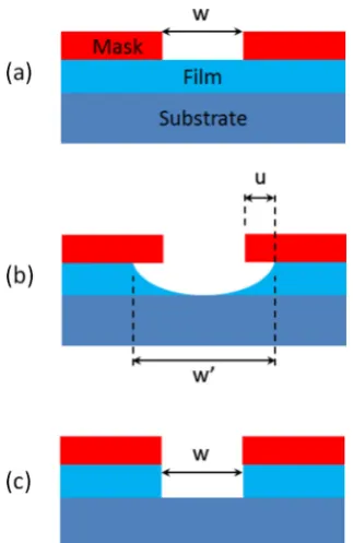
‘lift-off’techniques [9] and through-mask plating [9,10], and these are often the preferred methods for patterning thick gold structures. Subtractive methods can be broadly classified as either wet or dry etching methods [11]. In these techniques, the metal film is covered with a lithographically patterned mask material (Fig.1a) and then exposed to a liquid or gas-phase etchant. Etching is typically used to fabricate micron-sized features, but by using high-resolution stepper or e-beam lithography, it can be extended to the submicron domain to produce nanoscale devices [11].
T. A. Green (*)
INEX, University of Newcastle, Herschel Annex Building, Newcastle upon Tyne NE1 7RU, UK
Traditionally, thin film patterning was performed by wet etching, but a disadvantage of this approach is that the etch usually proceeds isotropically and the mask is undercut (Fig.1b). The resulting loss in feature size became a serious issue when the dimensions of the etch features approached 3– 5μm, and at this stage, wet etching was largely abandoned in the semiconductor industry and replaced by dry etching methods [11]. In contrast to the action of wet etchants, dry etching is highly anisotropic and results in minimum undercut (Fig.1c). However, for etching larger structures, wet etching is still useful and more cost effective. In addition, some metals are difficult to dry etch, and for this reason, the wet etching of gold, copper and platinum is still widely used.
In the following sections, dry and wet methods of pattern-ing gold thin films for microfabrication are critically reviewed. Dry methods are discussed first, with a particular emphasis on reactive ion (plasma) etching. This is followed by an analysis of wet etching techniques using various aqueous and non-aqueous etchants.
Dry etching
The term‘dry etching’ encompasses a wide range of gas-phase physical and chemical processes that can be used to remove material from a substrate or thin film [8,11]. Exam-ples of the former include ion beam milling and sputter etching where material is removed by bombarding ions break-ing surface bonds and ejectbreak-ing atoms. At the other extreme are
purely chemically driven processes where an etch species adsorbs on the surface to form a volatile product which can then escape into the gas phase. However, from the point of view of microfabrication, the most useful dry etching tech-nique is reactive ion etching (RIE) [12–14]. In this process, both physical and chemical processes operate cooperatively to remove material, and it is suitable for etching a wide range of metals, polymers, dielectrics and semiconductor materials.
Overview of reactive ion etching
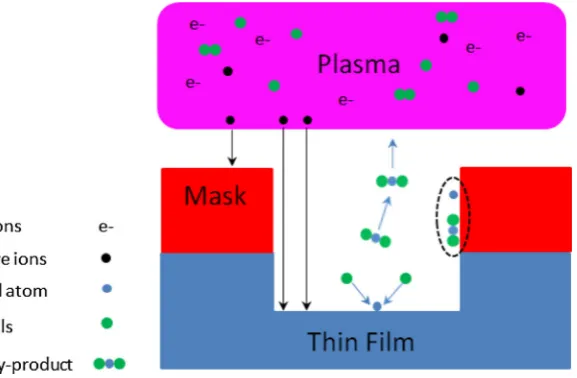
The basic principles of reactive ion etching [12–14] are shown schematically in Fig.2. Initially, the substrate to be etched is placed in a reactive plasma which contains the etchant gases. It is also patterned with a masking material so that only certain sections of the surface are etched. The function of the plasma is to generate reactive species (radicals and ions) which can assist with the removal of material. Reactive species are transported from the gas phase to the surface where they form volatile products which then desorb and are pumped away. Concurrently, the plasma generates ionic species which bom-bard the surface, breaking chemical bonds and ejecting atoms. This process also enhances chemical etching so that a more accurate description of the overall etch process ision-assisted etchingrather than reactive ion etching [12,13]. The direction of the bombarding ions is normal to the etch surface so that ion-assisted etching occurs mainly at the bottom of the feature rather than on the sidewalls. This leads to an essentially anisotropic etch profile with little undercut of the mask.
A wide range of RIE systems have been developed [12–14], but a commonly used configuration is the inductively coupled plasma (ICP) etcher shown in Fig.3. In this system, a low pressure, high-density radio-frequency (RF) plasma is generated in the process chamber using a surrounding induc-tive coil. The process gases are injected into the chamber by mass flow controllers, and volatile products are removed from the chamber via the pumping system. The chamber pressure is usually maintained at a few millitorr. The wafer substrate is mounted on a‘chuck’which is designed to keep the substrate at a near-ambient temperature during the etch process. In the case of etching non-volatile materials (e.g. Cu, Pt and Au), it is advantageous to use a heated chuck to maintain the wafer at an elevated temperature (e.g. 100–250 °C) [14]. RF power is also supplied separately to the substrate (‘platen’) so that the ener-gy of the bombarding ions can be independently controlled. In terms of controlling the etch process, the most important parameters are the gas flow rates, chamber pressure, RF power and temperature.
Reactive ion etching of gold
Although dry etching methods are usually the preferred means of patterning metal films for microfabrication, there are a Fig. 1 Examples of various etch profilesamasked substrate with feature
[image:2.595.89.251.50.299.2]number of issues which restrict their application to gold metallisation. For example, a key requirement of a good etch process is that the reaction products are volatile and can be easily removed from the surface to the gas phase [12,13]. For the RIE of metals, chlorine (Cl2or BCl3) or bromine (HBr) etch
chemistries are often used because many metals such as alu-minium and titanium form volatile halide compounds (Table1). During the chlorine etching of aluminium, Cl radicals generat-ed in the plasma react to form the volatile AlCl3species as
follows:
Cl2 ⇔ 2Cl ð1Þ
Alþ3Cl ⇔ AuCl3ð Þg ð2Þ
However, in the case of gold, the main reaction product, AuCl3, has a low vapour pressure at normal etch temperatures
(Table1) [15]. The low volatility of AuCl3can be
compen-sated by increasing the temperature, but above∼130 °C, the AuCl3species (which exists as the dimer Au2Cl6in the vapour
phase) decomposes to Au2Cl2and finally to non-volatile AuCl
[15]. This reaction scheme can be represented as:
Auþ3Cl ⇔ AuCl3ð Þs ð3Þ
2AuCl3 ⇔ Au2Cl6ð Þg ð4Þ
Au2Cl6ð Þg ⇔ Au2Cl2ð Þ þg 2Cl2 ð5Þ
Au2Cl2ð Þg ⇔ 2AuCl sð Þ ð6Þ
For this reason, the etch temperature needs to be carefully controlled to maintain the volatility of AuCl3while avoiding
its thermal decomposition to AuCl [16].
Another consequence of the low volatility of AuClxspecies
is the tendency for etched gold to redeposit elsewhere on the substrate and in the process chamber [17,18]. This is highly undesirable as it leads to contamination of the wafer and necessitates frequent chamber cleaning [18]. A related phe-nomenon is that of low volatility etch products redepositing on the sidewalls of the etch mask during the etch process [16, 17]. This can arise from ion-induced sputtering of the non-volatile etch product that forms on the surface and also by direct condensation of etch by-products. The resulting de-posits are known as‘fences’or‘veils’and are often difficult to remove in subsequent processing steps [17,19]. This prob-lem is particularly severe when a thick photoresist mask is used as a mask. A common solution to this problem is to use a
‘hard’mask (e.g. SiO2) which is typically much thinner and
tends to minimise the amount of redeposition [16,19]. Initial attempts at reactive ion etching of gold films were performed in the 1980s and 1990s using low-density plasma Fig. 2 Illustration of
fundamental processes occurring during reactive ion etching. The dotted areashows a region where non-volatile material has deposited on the sidewall of the mask
[image:3.595.258.547.54.243.2] [image:3.595.277.545.545.695.2]etch systems (Table2). A very early study was by Mogab and Shankoff [20] who examined the RIE of gold in the context of patterning a Ti-Pd-Au metallisation stack. Using a parallel plate RIE tool and a CClF3plasma, they obtained an etch rate
of 25 nm/min but observed severe problems with gold redepositing across the wafer surface. In 1993, Ranade et al. [21] performed a detailed investigation of the RIE of gold films using Cl2, CF4and CCl4. A relatively low etch rate of
3 nm/min was observed for etching in pure Cl2, but a rate of
100 nm/min was obtained in an optimised CCl4/CF4mixture.
Gold line-widths of 3 μm where achieved with good edge definition and minimal undercut. For the mixed gas process, the etch selectivity for photoresist and SiO2masks were 2:1
and 4:1, respectively.
In a later paper, Aldridge [16] used a parallel plate RIE tool to etch Au in a Cl2plasma using a SiO2hard mask. In initial
experiments performed at 75 °C, gold redeposition on the mask surface was observed due to the relative low vapour pressure of the AuCl3etch product. At 125 °C, the vapour
pressure was sufficiently high that redeposition was not ob-served, but at 150 °C, gold formed on the feature sidewalls— possibly due to the formation of AuCl. Replacing the SiO2
mask with a thick photoresist mask also resulted in gold redeposition on the mask sidewalls. Under optimum
conditions, an etch rate of 980 nm/min was achieved, and features as small as 0.5μm with etch depths of 5μm could be obtained with vertical sidewalls and minimal undercutting.
A more recent study of gold etching using a parallel plate RIE tool and a CF4/Ar plasma was performed by Kang and
co-workers [22]. Using a design of experiments approach, they were able to optimise the etch process. A maximum etch rate of 56 nm/min was obtained, and the sidewall profile was approximately 70°. As the expected etch by-product, AuFx,
has a very low volatility, it is likely that etching mechanism is entirely physical, arising from argon ion sputtering of the AuFxlayer.
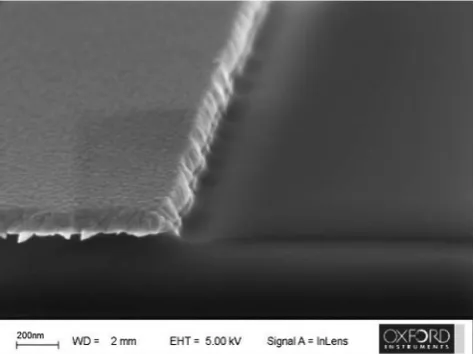
From the period of the late 1990s to the present, conven-tional RIE tools were largely replaced with high-density plas-ma equipment [12–14]. As well as inductively coupled plasma systems, electron cyclotron resonance (ECR) etchers were also introduced, and most recent work on gold etching has employed either ICP or ECR tools (Table2). These allowed many improvements in etch performance, but the fundamental issues associated with the available halogen-based etch chem-istries meant that the RIE of gold continued to be problematic. However, one advantage of the new high-density plasma etchers was that they operated at a much lower pressure than earlier parallel-plate RIE systems, and this tended to minimise redeposition and associated fencing issues [23]. Figures4and 5show examples of the ICP etching of gold thin films where redeposition effects are negligible.
[image:4.595.50.290.80.179.2]An early high-density plasma study by Ohtake et al. [24] utilised an ECR reactor and a chlorine-based plasma chemis-try to etch gold and aluminium films. The plasma discharge was maintained from a microwave source, while separate RF power was supplied to the platen. Initial experiments run with a continuous source power resulted in etch rates of 150 nm/ min, but gold redeposition on the sidewalls of the mask was noted. However, by pulsing the source power (i.e. 30μs on/off cycles), a higher etch rate of 260 nm/min was obtained Table 1 Vapour pressures of chlorine etch products at various
tempera-tures [12,15]
Substance Temperature (°C)
0.01 Torr 0.1 Torr 1 Torr
AuCl3 150 185 220
AuCl 520 680 920
AlCl3 57 77 99
TiCl4 −68 −45 −16
Table 2 Summary of process conditions for the reactive ion etching of gold
RIE system Etch gases RF powera/W Pressure/mT Temp (°C) Etch mask Etch profile Etch rate (nm/min) Ref
PP CClF3 200 350 85 – – 25 [20]
PP CF4/CCl4 450 150 25 SiO2, PR – 99 [21]
PP Cl2 400 100 125 SiO2 85° 980 [16]
PP CF4/Ar 375 32 – PR 70° 56 [22]
DF Cl2/Ar – 2 – PR 75° 35 [19]
ECR Cl2 1,000/100 2 80 PR – 250 [24]
ICP Cl2/Ar 700/– 15 30 SiO2 65° 350 [25]
ICP Cl2/Ar 600/250 2 20 PR – 70 [28]
ICP H2 500/100 20 10 SiO2 – 26 [29]
PPparallel plate,DFdual frequency,ICPinductively coupled plasma,ECRelectron cyclotron resonance
a
[image:4.595.49.553.545.688.2]without significant redeposition. It was suggested that the enhancement in etch performance was due to the production of additional negative ions under pulse conditions.
In 1999, Werbaneth and co-workers [19] reported the RIE of Au thin films using a dual-frequency magnetically confined etch reactor. Using a photoresist mask and HBr/Ar and Cl2/Ar
etch chemistries, it was found that gold redeposited along the mask sidewalls forming veils or fences. However, after optimising the Ar/Cl2 process, a maximum etch rate of
350 nm/min was obtained with negligible gold redeposition and a 75° etch profile. The use of a thin hard mask was also found to be effective in eliminating gold redeposition. The corresponding HBr/Ar process gave lower etch rates and more severe gold redeposition but produced a more vertical etch profile due to improved sidewall passivation.
Franz et al. [17] reported the reactive ion etching of a Ti/Pt/ Au ohmic contact using a high-density plasma etcher and a variety of etch chemistries. The top Au layer was etched using
a thin Al2O3hard mask or a thick photoresist. Using Cl2or
BCl3, gold etch rates of 1–4 nm/min were obtained, with Cl2
typically etching three times faster. The RIE etch profile was free of redeposited material, whereas attempts to sputter etch the gold layer resulted in fences forming on the resist edges.
The etching characteristics of gold films using an ICP etcher and a Cl2/Ar-based chemistry were examined by Chang
et al. [25] in 2003. The highest etch rate of 350 nm/min was observed at a Cl2/(Cl2+Ar) ratio of 0.20, and the selectivity to
a SiO2mask was 4:1. The etch rate was 15 % higher than in a
pure Ar plasma, indicating that etching occurred by a combi-nation of ion-assisted chemical reactions and physical sputtering, with the latter being the dominate process. XPS analysis of the etched surface showed the existence of Au-Cl bonds, indicative of the presence of a non-volatile AuClxetch
by-products. In subsequent papers [26,27], these results were used to develop a mechanism and comprehensive etch model for this system.
More recently, Aydemir and Akin [28] studied the etching of gold using a dual-frequency ICP etcher and HBr/Ar and Cl2/Ar chemistries. Redeposition of gold was observed on the
resist sidewalls under all etch conditions and was dependent on the thickness (and profile) of the resist etch mask and also the process parameters (e.g. coil and platen RF powers). Gold redeposition was worse for the HBr/Ar plasma than for Ar/Cl2
but even in the latter case could not be eliminated entirely. Eventually, the redeposition was eliminated by depositing a thin titanium film on top of the photoresist mask. This is a useful approach when traditional methods of preventing redeposition (i.e. use of thin hard mask [16, 19]) are not feasible.
The various issues associated with halogen etching of gold have led to the investigations of other possible etch chemis-tries. One promising approach is the use of a H2plasma which
has previously also been used to etch‘difficult’materials such as copper and silver. In the study of Hess and co-workers [29], the etching of gold film in an ICP reactor using a SiO2hard
mask and H2, He and Ar plasmas was explored. Etch rates of
55 nm/min for He, 62 nm/min for Ar and 26 nm/min for H2
plasmas were reported. For Ar and He, etching occurs pre-dominantly by a sputtering process, but the low mass of hydrogen species indicates that observed etch rate must also have a chemical aspect. This would presumably occur by the formation of hydride species, but both AuH and AuH2− are
known to have limited thermodynamic stability [29].
Wet etching
In contrast to many other metals, wet etching of gold is still an important process in microfabrication. This has partially aris-en because of the difficulties in patterning gold by dry etching, but also reflects the inherent advantages of wet etching Fig. 4 ICP etching of Au film in Cl2plasma at 160 °C (SiO2hard mask
has not been removed)
Fig. 5 ICP etching of 100 nm Au film in Cl2plasma at room temperature
[image:5.595.53.290.52.230.2] [image:5.595.52.290.513.690.2]including low equipment costs, low energy usage and high throughput [30,31]. The isotropic nature often makes it un-suitable for fine pattern delineation, but for many applications, feature sizes are typically in the range of 10–100 μm and masks can usually be biased to compensate for significant undercut [11]. Table 3 summarises the relative advantages and disadvantages associated with dry and wet etching. As well as its use in device fabrication, wet etching is an impor-tant technique in the failure analysis of microelectronic com-ponents [32] and also in the recovery/recycling of gold from scrap electronic products [33].
Etching solutions for gold contain two essential compo-nents [34]. Firstly, a complexing ligand is needed as it is not thermodynamically possible to dissolve gold without forming stable Au(I) complexes [35, 36]. Suitable ligands for gold etching include cyanide, chloride, iodide, bromide, thiosulfate and thiourea. Secondly, an oxidant is needed to establish the potential of the surface at a value where significant gold dissolution can occur [31]. The oxidant and ligand (and their concentrations) must be carefully chosen so that a reasonable etch rate can be attained while avoiding the possibility of passivating the gold surface [35,36]. As well as these constit-uents, the etchant may also contain other components such as stabilisers, inhibitors, wetting agents and pH buffers [30].
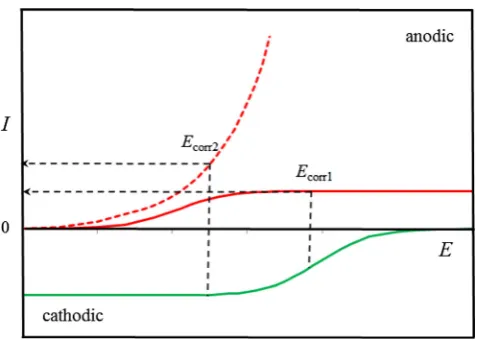
Wet etching is electrochemical in nature (essentially a controlled corrosion process), and it can be analysed in terms of Wagner and Traud’s mixed potential theory [37]. In this model, the oxidation (etching) and reduction reactions occur simultaneously on the metal surface (Fig.6). For the anodic reaction, Au metal is oxidised to Au+ at the metal-solution interface and then forms a complex with ligand (L−). In the cathodic process, the oxidant is reduced at the same interface and consumes the electrons generated by the anodic reaction. In the absence of an externally applied potential or current, the system will adopt an equilibrium potential where the rates of the two reactions are equal. This potential is known as the
mixedorcorrosionpotential,Ecorr. The observed etch rate is
determined by the anodic current density, Icorr, that
corre-sponds to the value of the corrosion potential.
The anodic and cathodic processes can be conveniently represented by individual polarisation curves (Figs.7and8), but the exact dependence of the current,I, on the potential,E, will depend on various thermodynamic, mass transport and kinetic considerations [11, 31]. Under kinetic control, the current depends exponentially on potential, but if mass trans-port constraints become imtrans-portant, a limiting current plateau is observed. In Fig.7, the corrosion potential occurs at a value where both the cathodic and anodic reactions are kinetically controlled. In Fig.8, the anodic reaction is shown to be under either kinetic or mass transport control, while the cathodic reaction is under mass transport control. The overall corrosion rate can therefore be controlled by mass transport limitations related to the diffusion of the ligand or oxidant to the surface, and the etch rate will be influenced by solution agitation [11]. By performing such an analysis of the current potential be-haviour of the individual reactions, it is possible to rationalise many aspects of the etching process.
The process of wet etching is relatively simple [30,38,39]. Firstly, the substrate is patterned with an etch mask. This is typically a photoresist material patterned lithographically, but Fig. 6 Fundamental electrochemical processes occurring during the wet etching of gold
[image:6.595.348.501.53.199.2]Fig. 7 Polarisation curves for an etching process where the anodic and cathodic processes are both under kinetic control
Table 3 Comparison of wet and dry etching methods
Dry etching Wet etching
Environment Vacuum Solution
Etch rate 0.01–0.1μm/min 0.1–1μm/min
Etch selectivity High High
Etch profile Anisotropic Isotropic
Etch resolution <1μm >3μm
Throughput Low (single substrate) High (batch)
Equipment cost High Low
Chemical usage Low High
[image:6.595.302.545.509.690.2] [image:6.595.52.288.572.714.2]masks consisting of self-assembled monolayers have also been used [40]. Unlike in dry etching, there is little erosion of the mask during the process, and the thickness is often not critical. Usually, the substrate(s) to be etched are immersed directly in the etchant solution, but spray etching systems are also common [30,38]. The temperature and agitation of the etchant solution must be carefully controlled as the etch rate may depend on these parameters. For etch processes under transport control, the degree of agitation must be constant over the entire substrate to ensure uniform etching. This can be difficult to achieve with immersion etching employing me-chanical stirring, and spray etching is often better in this regard [30]. The completion of the etch process can usually be determined visually or by using an optical end-point sys-tem, but for opaque solutions, timed etches are necessary.
A common concern in wet etching is minimising the extent of undercutting. This is inevitable for an isotropic process but will depend strongly on the prevailing etch conditions. Exces-sive undercut is often due to the mask becoming partially detached from the underlying film resulting in enhanced lat-eral etching [30]. Such peeling back of the mask may arise due to poor adhesion of the mask to the film and/or high internal stress [30,38,39]. It should be noted that the adhesion of photoresist masks to gold is often quite poor as conventional adhesion promoters (e.g. HMDS) are not effective for metals which do not form a surface oxide. In the case of etching metal films in contact with a second metal, various electrochemical effects can also occur to increase undercutting (Galvanic effects in Au etching section).
Considering that a very large number of gold etchants have been developed, the discussion in the following sections is restricted to systems that are widely used and/or have been systematically studied. A 1985 review by Norrman and Stripple [34] evaluated a number of gold etchants, and details
on many others can be found in a number of standard compi-lations of etch recipes [11,38,39,41–43].
Aqueous etchants
The most well-known etchant for gold is a mixture of concen-trated hydrochloric and nitric acid, known asaqua regia[44]. The overall reaction for gold dissolution can be given as:
Auþ4HþþNO3−þ4Cl−→AuCl4−þNO gð Þ þ2H2Oð7Þ
The potency of the etchant tends to decline with time due to the formation of volatile products such as NOCl and Cl2.
Whileaqua regiais capable of dissolving gold at a very high rate (∼10 μm/min [39, 41]), its corrosiveness toward other materials and general instability make it impractical for use in microfabrication. Dilution ofaqua regiawith water produces a slower and more practical etchant that is compatible with some photoresists, but etch stability is still an issue [42].
A more useful gold etchant is the alkaline cyanide system, which is used extensively for the hydrometallurgical extrac-tion of gold [45]. This etchant is usually formulated from NaCN or KCN salts with O2, H2O2 or Fe(CN)63− as the
oxidant [34]. They are usually operated in the alkaline region (pH>10) to avoid the formation of HCN gas. The correspond-ing anodic and cathodic reactions in oxygen-containcorrespond-ing solu-tions are:
Auþ2CN−→Au CNð Þ2−þe‐ ð8Þ
O2þ2H2Oþ4e−→4OH− ð9Þ
Representative polarisation curves for these two reactions and the resulting mixed potentials are shown in Fig.8. If the cyanide concentration is low, then the anodic reaction is under mass transport control and a limiting current is observed. At higher concentrations, it is under kinetic control, and the current increases exponentially with potential. For the reduc-tion reacreduc-tion, the concentrareduc-tion of dissolved O2is also low so
that this reaction can also be under mass transport control. The temperature dependence of the gold dissolution rate in aerated cyanide solutions corresponds to an activation energy of 8– 20 kJ/mol [45] which is indicative of an anodic or cathodic mass transport controlled process [46].
There are a number of reports [34, 40, 47, 48] of using cyanide etchants to pattern thin gold films, and MacArthur [47] has reported an etch rate of 60 nm/min in an etchant comprising 0.4 M K3Fe(CN)6, 0.2 M KCN and 0.1 M KOH.
In some cases, the use of cyanide has been found to be superior to iodine-iodide system in terms of surface Fig. 8 Polarisation curves for an etching process where the anodic
reaction is under mass transport (solid line) or kinetic control (dotted line). In the first case, the corrosion rate is determined atEcorr1. In the
latter case, the corrosion rate is determined byEcorr2, and the etching
[image:7.595.51.290.50.220.2]roughness, feature definition and degree of undercutting [34, 48]. It is also compatible with the use of photoresists and self-assembled monolayers as etch masks [40], and the transpar-ency of the solution allows a convenient visual endpoint. Despite these advantages, the high toxicity of cyanide and corresponding issues with disposal have severely curtailed its use. However, it is still commercially available, and it is often the preferred etchant when fine pitches are required and min-imal undercut can be tolerated [49].
The most commonly used etchant for patterning gold is undoubtedly the iodine-iodide system [7,32,34,48,50]. This is typically formulated from KI or NaI salts and I2[34,50].
The oxidant in this system is the triiodide ion (I3−) formed by
the reaction of I2 with I−. The corresponding anodic and
cathodic reactions are:
Auþ2I−→AuI2−þe− ð10Þ
I3− þ2e−→3I− ð11Þ
Under normal etching conditions, the anodic and cathodic reactions are expected to be under kinetic control (Fig.7) with the etch rate largely independent of agitation rates [47]. The temperature dependence of the etch rate for commercially available iodine-iodide etchant [51] yields an activation ener-gy of∼35 kJ/mol, indicative of a kinetically controlled process [46].
A typical formulation of this etchant is 0.6 M KI or NaI and 0.2 M I2which gives an etch rate of 0.5–1μm/min at room
temperature [34,39]. This is suitable for fast etching of thick gold films, but for thinner films, it is usually diluted further to bring it into the range of 50–200 nm/min. This solution also etches Al, Ni, and NiCr at an appreciable, rate and commercial formulations often contain inhibitors (e.g. phosphate com-pounds) to minimise the attack on these metals [52,53]. The etch is easy to prepare, has low toxicity and operates in a near-neutral pH range. It also has good compatibility with positive and negative photoresists but not with alkanethiol SAM resists [40]. Etch performance is generally good (Fig.9), but some issues with non-uniformity, staining and abnormal undercut-ting have been noted [18,32,34,48,50]. Another issue is that the etchant is opaque which makes it difficult to judge when the etch process is complete [42]. There is one report [54] of gold etching in bromine-bromide solutions. It has similar etch characteristics to the iodine-iodide system, but the greater toxicity and high vapour pressure of bromine are obvious disadvantages.
The environmental impact of etchants containing cyanide, bromine and strong acids is obviously high, but the iodine-iodide system represents fewer concerns relating to health and safety and chemical disposal. In addition, a number of
methods [55,56] have been developed for iodine-based etch-ants which allow gold recovery and etch regeneration so the sustainability of the process is good.
Another gold etchant which has been proposed is the thiosulfate system formulated from K2S2O3and KOH and
using K3Fe(CN)6as an oxidant [57]. These etchants are
usu-ally operated in the alkaline region as thiosulfate ions as unstable at pH<10 [3]. The electrochemical reactions occur-ring at the gold surface are:
Auþ2S2O32−→Au Sð 2O3Þ2
3−þe− ð12Þ
Fe CNð Þ63− þe−→Fe CNð Þ64− ð13Þ
[image:8.595.308.545.52.232.2]This formulation has been used to etch gold films that had been patterned with self-assembled monolayers using Fig. 9 Wet etching of 20-μm-wide gold feature in a standard iodine-iodide etchant. The gold thickness is 100 nm
[image:8.595.334.506.506.692.2]microcontact printing. This etchant resulted in fewer defects, better edge definition and a higher etch rate than for cyanide-based etchants. Etch rates are typically low (<10 nm/min), and the solutions have limited stability. In order to address this, the benzene thiosulfonate ligand was used in place of thiosulfate [58]. This etchant was more stable but produced a greater number of etch defects. All these etchants operate at a pH≈ 14, which is suitable for SAM masks but is incompatible with positive photoresists and many substrates.
Electrochemical etching
A related technique for patterning thin metal films is electro-chemical etching or‘deplating’[18,59,60]. In this approach, an external current or potential is used to drive the anodic dissolution process rather than relying on the action of oxidising agents. The etch solution still requires a ligand to form soluble complexes, and an underlying conductive layer (e.g. TiW) is also necessary to supply the current. One advan-tage of this approach is that, by careful consideration of current distribution and mass transport effects, it is possible to achieve a more anisotropic etch profile (i.e. reduced under-cutting) than for conventional wet etching [61].
Hu and Ritzdorf [59] demonstrated the use of electrochem-ical etching to remove gold seed layers following through-mask plating—a process that is normally performed by wet etching. An etch system similar to a conventional‘fountain’ wafer plater was used, and this allowed the hydrodynamic conditions, current distribution and temperature to be precise-ly controlled. While etching in acid chloride solutions left behind residues, the use of iodide with a sulfite stabiliser
resulted in complete removal of gold and with negligible undercutting. Electrochemical etching of Au seed layers in thiourea solutions has also been investigated, but due to local variations in the etch rate, it was difficult to develop a stable and repeatable process [18]. More recently, selective removal of gold thin films in chloride media using electrochemical etching has also been used to successfully fabricate RF MEMS devices [60].
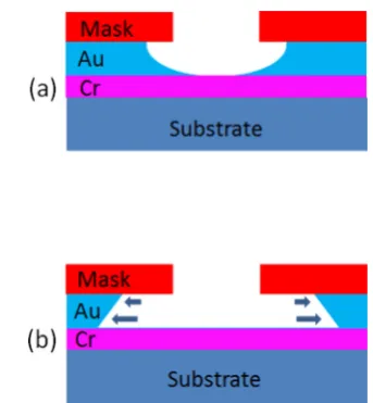
Galvanic effects in Au etching
Wet etching of gold usually results in an isotropic profile (Fig.10a), but in the presence of another metal, a vertical or reentrant profile with much greater undercut is often observed (Fig.10b). This typically occurs when etching a gold film with an underlying adhesion layer of Cr, Ti or TiW. Such effects have been noted by a number of authors [34,48,50], and it is thought to be caused by the two metals forming a galvanic couple. Usually, it is found that the etch proceeds in a normal isotropic manner, but just at the point where the gold disap-pears and the under-layer is exposed to the solution, the lateral etch rate increases rapidly [48].
[image:9.595.53.290.52.163.2]This effect can be understood as follows [11,30]. Initially, the oxidation and reduction reactions proceed on the Au surface exposed to the etchant. However, after the Au is fully etched and the under-layer metal is exposed, the cathodic process can usually be sustained on that surface (and also on the remaining Au on the etch sidewalls), and the available area is unchanged. In contrast, the only remaining Au surface for the oxidation reaction to occur is on the sidewalls, and this area will be typically much lower than the original Au area. So while thecurrentthrough the anodic element will be similar to that which prevailed at the beginning of the etch, thecurrent density will be much higher. It is this area effect which is mainly responsible for the observed acceleration in etch rate. Such galvanic effects have been mainly observed for etch-ing in iodine-iodide solution, but not for the cyanide systems [34,48]. In the latter case, the maximum current density that can pass through the anodic element is usually controlled by mass transport (Fig.8). This will certainly be the case if the cyanide concentration in solution is kept relatively low. The use of mass transport limitations to minimise galvanic under-cut has been exploited in many other etch systems [62]. For the iodine-iodide system, the etch composition, nature of the Fig. 11 Images of wet etching profiles for Au films etched in iodine
etchant under different conditions [50].aNormal isotropic profile andb reentrant profile due to galvanic effects.R+denotes the photoresist mask. Reproduced by permission of The Electrochemical Society
[image:9.595.237.545.624.709.2]under-layer metal and etch mode (i.e. spray versus immersion) all influence the amount of galvanic undercut (Fig.11), but usually it cannot be eliminated entirely [50].
Nonaqueous etchants
Given the limitations associated with some aqueous-based gold etchants, various attempts have been made to develop non-aqueous alternatives. For example, Bigoli et al. [63] have developed a range of powerful oxidising agents capable of dissolving gold in tetrahydrofuran (THF) solutions. In an initial study, they prepared the bis-diiodine adduct of N,N′ -d i m e t h y l p e r h y -d r o -d i a z e p i n e - 2 , 3 - -d i t h i o n e l i g a n -d (Me2dazdt.2I2). This new etchant was successfully used to
remove thin gold layers from GaAs laser diodes for the purpose of failure analysis [64]. In a subsequent paper by this group, the iodine-bromine adduct of N,N′ -dimethylperhydrodiazepine-2,3-dithione was synthesised (Me2dazdt.2IBr) [65]. In this
etchant, the main reaction product is a Au(III) square planar complex, and the overall reaction for the dissolution of gold is shown in Fig.12. This new oxidant etched gold at a higher rate (∼50 nm/min) than the diiodine adduct and was comparable to that found for aqueous iodine-iodide etchants. These non-aqueous etchants were also found to produce a cleaner and more uniformly etched surface.
In a 2013 study, this group described gold etching using iodine tetraethylthiuram disulfide (Et4TDS) mixtures in acetone
[66]. Trials on Ti/Au metallised silicon wafers indicated uni-form etching with a rate of ca. 30 nm/min. The dissolution of gold powder in thioamide-I2 adducts has also been reported
recently [67]. The best results were obtained using iodine adducts of 3-methyl-benzothiazole-2-thione (mbtt) in diethyl ether solvent, but the etch rate was not determined. One
important advantage of Et4TDS and mbtt is that they are
relatively inexpensive compared to the original Me2dazdt
reagent.
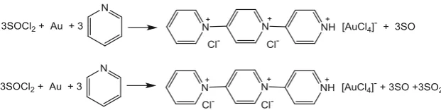
Lin and co-workers [68] have recently formulated etchants consisting of mixtures of thionyl chloride (SOCl2) and organic
solvents such as pyridine and N,N-dimethyl formamide (DMF). Such formulations that can etch gold at moderate rates and have been referred to as‘organic aqua regia’. Using a 3:1 SOCl2/pyridine mixture, gold could be etched at a rate of
50 nm/min at room temperature. Silver and palladium could also be dissolved in the etchant, but platinum was found to be inert. The overall etch mechanism is unclear, but for gold dissolution, the main reaction product is AuCl4−, and the
reaction scheme shown in Fig.13has been proposed. In a related study, Räisänen et al. [69] reported the disso-lution of thiol-functionalised gold in alcohol sodisso-lutions. By attaching 4-pyridinethiol to the gold surface, uniform dissolu-tion was observed in both methanol and ethanol solvents. The dissolution mechanism involves the formation of soluble Au(I) thiolato complex and is mediated by dissolved oxygen. These complexes have low solubility, and gold precipitation during etching has been observed. The technique has also been used to produce free-standing nanometre-thick Au foils, but the etch rate is extremely slow, typically requiring a few days to dissolve a 100-nm-thick Au film.
[image:10.595.232.543.53.131.2]While all these non-aqueous etchants all have some indus-trial potential, there are a number of issues that need to be addressed. Firstly, the presence of certain solvents (e.g. acetone, methanol, DMF) makes them incompatible with photoresist materials so that if the gold needs to be patterned, only hard masks can be used. More importantly, many of the etchants contain hazardous solvents (e.g. pyridine, DMF), while re-agents like SOCl2are also potentially dangerous. In terms of
Fig. 13 Probable reaction scheme for the dissolution of gold in SOCl2/pyridine mixtures
(‘organic aqua regia’) [68]
Table 4 Comparison of some aqueous and non-aqueous gold etchants
Etchant [ref] KCN/O2[34] KI/I2[34] Me2dazdt.2IBr [65] Et4TDS/I2[66] SOCl2/py [68]
Solvent Water Water THF Acetone Pyridine
Etch rate 0.05–1μm/min 0.05–1μm/min 0.03μm/min 0.05μm/min
Undercut Low High – – –
Mask Photoresist Photoresist Hard Hard Hard
Toxicity High Low Low Low High
Cost Medium Low High Low High
[image:10.595.51.549.597.701.2]addressing environmental and safety concerns, the iodine-based non-aqueous etchants [66] seem to be the most appro-priate. Issues regarding the cost of materials and environmental disposal will also need to be considered before any of these etchants can be adopted. Table4summarises the various attri-butes of selected aqueous and non-aqueous gold etchants.
Conclusions
The etching of gold is an important technology in the fabri-cation of many microdevices, and over the last few decades, considerable advances in both the understanding and practical application of this technique have been made. Dry methods which utilise reactive ion etching have a number of important advantages over other methods, but the low volatility of gold etch products is a key problem. However, the intro-duction of high-density plasma reactors with optimised chlorine-based chemistries has allowed improved process-es to be developed, and alternate plasma chemistriprocess-es (e.g. hydrogen) are also being explored. The use of heated chucks to improve the volatility of gold etch products is another possible solution, but care needs to be taken to avoid the formation of other non-volatile products at elevated temperatures.
Significant progress in the development of wet etchants for gold has also been made. Traditionally, iodine- and cyanide-based etch processes have been used, but due to toxicity of the latter, it is only used in a few niche applications. The dominant gold etchant is iodine-iodide, and while it is satisfactory for most applications, it has some process issues and is particu-larly prone to undercutting arising from galvanic effects. The introduction of microcontact printing using self-assembled monolayers as etch masks had also led to the development of various new gold etches which are compatible with these materials. The use of electrochemical etching has also been explored, and for applications such as gold seed layer removal, it has some advantages over con-ventional wet etching. Finally, in the last decade there has been considerable work on the development of various non-aqueous etchants, and once issues relating to chemical handling, disposal and costs have been addressed, these etchants may become viable alternatives to aqueous etchants.
Acknowledgments The author would like to thank Colin Welch and Owain Thomas at Oxford Instruments for providing the images shown in Figs.4and5.
Open AccessThis article is distributed under the terms of the Creative Commons Attribution License which permits any use, distribution, and reproduction in any medium, provided the original author(s) and the source are credited.
References
1. Holliday R, Goodman P (2002) Going for gold. IEE Rev 48:15–19 2. Christie IR, Cameron BP (1994) Gold electrodeposition within the
electronics industry. Gold Bull 27:12–20
3. Green TA (2007) Gold electrodeposition for microelectronic, opto-electronic and micro-system applications. Gold Bull 40:105–114 4. Williams R (1990) Modern GaAs processing methods. Artech
House, Boston
5. Varadan VK, Vinoy KJ, Jose KA (2003) RF MEMS and their applications. John Wiley & Sons, Chichester
6. Wooten EL, Kissa KM, Yi-Yan A, Murphy EJ, Lafaw DA, Hallemeier PF, Maack D, Attanasio DV, Fritz DJ, McBrien GJ, Bossi DE (2000) A review of lithium niobate modulators for fiber-optic communications systems. IEEE J Sel Top Quant 6:69–81 7. Eidelloth W, Sandstrom RL (1991) Wet etching of gold films
com-patible with highTcsuperconducting thin films. Appl Phys Lett 59:
1632–1634
8. Liu C (2006) Foundations of MEMS. Pearson Education, Upper Saddle River
9. Madou MJ (2002) Fundamentals of microfabrication: the science of miniaturization, 2nd edn. CRC Press, Boca Raton
10. Roy S, Gupte Y, Green TA (2001) Flow cell design for metal deposition at recessed circular electrodes and wafers. Chem Eng Sci 56:5025–5035
11. Köhler M (1999) Etching in microsystem technology. Wiley-VCH, Weinheim
12. Lieberman MA, Lichtenberg AJ (1994) Principles of plasma dis-charges and materials processing. John Wiley & Sons, New York 13. Chen FF, Chang JP (2002) Principles of plasma processing: a lecture
course, Kluwer Academic Publishers
14. Donnelly VM, Kornblit A (2013) Plasma etching: yesterday, today and tomorrow. J Vac Sci Technol A 31:050825–1–050825–48 15. Landsberg A, Hoatson CL (1970) The kinetics and equilibria of the
gold-chlorine system. J Less Common Metals 22:327–339 16. Aldridge FT (1995) High speed anisotropic reactive ion etching of
gold films. J Electrochem Soc 142:1563–1565
17. Franz G, Kachel R, Sotier (2002) Residual free reactive ion etching of the Bell contact Ti/Pt/Au. Mater Sci Semicond Process 5:45–50 18. Werbaneth P, Lester T, Pakulska J (2003) Removing gold seed-layer
materials using reactive ion etch. MICRO 21:47–55
19. Werbaneth P, Hasan Z, Rajora P, Rousey-Seidel M (1999) The reactive ion etching of Au on GaAs substrates in a high density plasma etch reactor. Available viahttp://gaasmantech.com/Digests/ 1999/PDF/12.pdfAccessed 6 April 2014
20. Mogab CJ, Shankoff TA (1977) Plasma etching of titanium for application to the patterning of Ti-Pd-Au metallization. J Electrochem Soc 124:1766–1771
21. Ranade RM, Ang SS, Brown WD (1993) Reactive ion etching of thin gold films. J Electrochem Soc 140:3676–3678
22. Kang TY, Kim G, Cho IH, Seo D, Hong SJ (2009) Process optimi-zation of CF4/Ar plasma etching of Au using I-optimal design. Thin
Solid Films 517:3919–3922
23. Delprat S, Chaker M, Margot J (2001) Investigation of the gas pressure influence on patterned platinum etching characteristics using a high-density plasma. J Appl Phys 89:29–33
24. Ohtake H, Samukawa S, Oikawa H, Nashimoto Y (1998) Enhancement of reactivity in Au etching by pulse-time-modulation Cl2plasma. Jpn J Appl Phys 37:2311–2313
25. Chang YS, Kim DP, Kim CI, Sim KB, Chang EG (2003) Etching characteristics of Au thin films using inductively coupled Cl2/Ar
plasma. J Korean Phys Soc 42:S791–S794
26. Efremov AM, Kim DP, Kim CI (2003) Etching characteristics and mechanism of Au thin films in inductively coupled Cl2/Ar plasma. J
27. Efremov AM, Kim DP, Kim CI (2004) Simple model for ion-assisted etching using Cl2-Ar inductively coupled plasma: effect of gas
mixing ratio. IEEE Trans Plasma Sci 32:1344–1351
28. Aydemir A, Akin T (2012) Prevention of sidewall re-deposition of etched by-products in the dry Au etch process. J Micromech Microeng 22:74004–74009
29. Choi TS, Levitin G, Hess DW (2013) Mechanistic considerations in plasma-assisted etching of Ag and Au thin films. ECS Solid State Technol 2:P275–P281
30. Romankiw LT (1976) Pattern generation in metal films using wet chemical techniques: a review. In: Hughes HG, Rand MJ (eds) ECS Proceedings of the Symposium on Etching for Pattern Definition. Princeton, The Electrochemical Society, pp 161–193
31. MacArthur D (1976) Chemical etching of metals. In: Hughes HG, Rand MJ (eds) ECS Proceedings of the Symposium on Etching for Pattern Definition. Princeton, The Electrochemical Society, pp 76–91 32. Mura G, Vanzi M, Stangoni M, Ciappa M, Fichtner W (2003) On the behaviour of the selective iodine-based gold etch for the failure analysis of aged optoelectronic devices. Microelectron Reliab 43: 1771–1776
33. Syed S (2012) Recovery of gold from secondary sources—a review. Hydrometallurgy 115–116:30–51
34. Norrman SH, Stripple H (1985) A theoretical and experimental study of chemical etching methods of the TiW-Au system for microwave hybrid applications. In: Proceedings of the International Symposium on Microelectronics, Anaheim, November 11–14 1985, pp 268–275, International Society for Hybrid Microelectronics
35. Nicol MJ (1980) The anodic behaviour of gold. Part 1—oxidation in acidic solutions. Gold Bull 13:46–55
36. Nicol MJ (1980) The anodic behaviour of gold. Part 2—oxidation in alkaline solutions. Gold Bull 13:105–111
37. Wagner C, Traud W (1938) On the interpretation of corrosion pro-cesses through the superposition of electrochemical partial propro-cesses and on the potential of mixed electrodes. Z Elektrochem 44:391–399 38. Burns DW (2011) MEMS wet-etch processes and procedures. In: Ghodssi R, Lin P (eds) MEMS materials and process handbook. Springer, New York, pp 457–665
39. Kern W, Deckert CA (1978) Chemical etching. In: Vossen JL, Kern W (eds) Thin film processes. Academic, New York, pp 401–496 40. Kumar A, Biebuyck HA, Whitesides GM (1994) Patterning
self-assembled monolayers: applications in materials science. Langmuir 10:1498–1511
41. Walker P, Tarn WH (eds) (1991) CRC handbook of metal etchants. CRC Press, Boca Raton
42. Williams KR, Gupta K, Wasilik M (2003) Etch rates for micromachining processing—part II. J Micromech Syst 12:761–778 43. Glang R, Gregor LV (1970) Generation of patterns in thin films. In: Maissel LI, Glang R (eds) Handbook of thin film technology. McGraw-Hill, New York, Chapter 7
44. Atkins P, Overton T, Rourke J, Weller M, Armstrong F, Hagerman M (2010) Inorganic chemistry, 5th edn. W.H. Freeman, New York, p 459
45. Marsden J, House CI (2006) The chemistry of gold extraction, 2nd edn. SME, Littleton
46. Power GP, Ritchie IM (1975) Metal displacement reactions. In: Bockris JOM, Conway BE, White RE (eds) Modern aspect of elec-trochemistry, 11th edn. Plenum Press, London, pp 199–250 47. MacArthur DM (1974) Technique for selective etching of gold and
etchant therefor. US Patent 3,846,196, 5 Nov 1974
48. Nemirovsky Y, Blech IA, Yahalom J (1978) Abnormal undercutting in etched Cr/Au films. J Electrochem Soc 125:1177–1179 49. Haberland J, Becker M, Lutke-Notarp D, Kallmayer C,
Aschenbrenner R, Reichl H (2010) Ultrathin 3D ACA
Flipchip-in-Flex Technology. IMAPS Device Packaging Conference, Scottsdale, 8–11 March 2010
50. Gabette L, Segaud R, Fadloun S, Avale X, Besson P (2009) Gold wet etch optimization on 200 mm substrates for MEMS applications. ECS Trans 25:337–344
51. Data for Transene TFA etchanthttp://www.transene.com/au_etchant. htmlAccessed 6 April 2014
52. Su KC, Lu HH, Chen CC, Moore JC (2008) Maximizing selectivity during wet-chemical gold etching. http://www.csmantech.org/ Digests/2008/2008%20Papers/17.1.pdfAccessed 6 April 2014 53. Licari JJ, Enlow LR (1991) Hybrid microcircuit technology
hand-book: materials, processes, design, testing and production, 2nd edn. Noyes, Westwood pp 97–98
54. Bahl SK, Leach GL (1980) Gold etchant composition and method. US Patent 4,190,489, 26 Feb 1980
55. Nguyen NV, Jeong J, Shin D, Kim BS, Lee JC, Pandey BD (2012) Simultaneous recovery of gold and iodine from the rinse water of the semiconductor industry using activated carbon. Mater Trans 53:760–765
56. Union RE (2009) Recovery of gold from potassium iodide-iodine etching solution. US Patent 7,582,136, 1 Sept 2009
57. Xia Y, Zhao XM, Kim E, Whitesides GM (1995) A selective etching solution for use with patterned self-assembled monolayers of alkanethiolates on gold. Chem Mater 7:2332–2337
58. Burdinski D, Blees MH (2007) Thiosulfate- and thiosulfonate-based etchants for the patterning of gold using micro-contact printing. Chem Mater 19:3933–3944
59. Hu Z, Ritzdorf T (2007) Cyanide- and thiourea-free electrochemical etching of gold for microelectronics applications. J Electrochem Soc 154:D543–D549
60. Sterner M, Roxhed N, Stemme G, Oberhammer J (2011) Electrochemically assisted maskless selective removal of metal layers for three-dimensional micromachined SOI RF MEMS trans-mission lines and devices. J Micromech Syst 20:899–908
61. Datta M (1998) Microfabrication by electrochemical metal removal. IBM J Res Dev 42:655–669
62. Kelly JJ, de Minjer CH (1975) An electrochemical study of under-cutting during etching of duplex metal films. J Electrochem Soc 122: 931–936
63. Bigoli F, Deplano P, Mercuri ML, Pellinghelli MA, Pintus G, Serpe A, Trogu EF (1998) A powerful new oxidation agent towards metal-lic gold powder:N,N’-dimethylperhydrodiazepine-2,3-dithione (D) bis(diiodine). Synthesis and x-ray structure of [AuDI2]I3. Chem
Commun 2351–2352
64. Vanzi M, Bonfiglio A, Salaris P, Deplano P, Trogu EF, Serpe A, Samini G, De Palo R (1999) Gold removal in failure anal-ysis of GaAs-based laser diodes. Microelectron Reliab 39: 1043–1047
65. Cau L, Deplano P, Marchio L, Mercuri ML, Pilia L, Serpe A, Trogu EF (2003) New powerful reagents based on dihalogen/N,N’ -dimethylperhydrodiazepine-2,3-dithione adducts for gold dissolu-tion: the IBr case. Dalton Trans 1969–1974
66. Serpe A, Marchio L, Artizzu F, Mercuri ML, Deplano P (2013) Effective one-step gold dissolution using environmentally friendly low-cost reagents. Chem Eur J 19:10111–10114
67. Isaia F, Aragoni MC, Arca M, Caltagirone C, Demartin F, Garau A, Lippolis V (2013) Gold oxidative dissolution by (thioamide)-I2
ad-ducts. Dalton Trans 42:492–498
68. Lin W, Zhang RW, Jang SS, Wong CP, Hong JI (2010) Organic aqua regia—powerful liquids for dissolving noble metals. Angew Chem Int Ed 49:7929–7932
![Table 1 Vapour pressures of chlorine etch products at various tempera-tures [12, 15]](https://thumb-us.123doks.com/thumbv2/123dok_us/1635645.116876/4.595.49.553.545.688/table-vapour-pressures-chlorine-products-various-tempera-tures.webp)

![Fig. 11 Images of wet etching profiles for Au films etched in iodineetchant under different conditions [50]](https://thumb-us.123doks.com/thumbv2/123dok_us/1635645.116876/9.595.237.545.624.709/images-etching-profiles-films-etched-iodineetchant-different-conditions.webp)