City, University of London Institutional Repository
Citation
:
Katrisku, Ferdinand Apietu (2000). Finite Element Study of the Second Order (X²) Nonlinear Process of Second Harmonic Generation in Optical Waveguides.(Unpublished Doctoral thesis, City, University of London)
This is the submitted version of the paper.
This version of the publication may differ from the final published
version.
Permanent repository link: http://openaccess.city.ac.uk/20273/
Link to published version
:
Copyright and reuse:
City Research Online aims to make research
outputs of City, University of London available to a wider audience.
Copyright and Moral Rights remain with the author(s) and/or copyright
holders. URLs from City Research Online may be freely distributed and
linked to.
linear Process of Second Harmonic Generation in
Optical Waveguides.
by
Ferdinand Apietu Katsriku
A thesis submitted to the City University for the Degree of Doctor of
Philosophy in Information Engineering
:
City University
Photonics Research Group, Department of Electrical, Electronic and
Information Engineering, Northampton Square, London ECl V OHB, UK.
Boston Spa, Wetherby West Yorkshire, LS23 7BQ www.bl.uk
PAGE NUMBERING AS
Table of contents List of Tables List of Figures Acknowledgements Declaration
Abstract
Symbols and Abbreviations
Chapter 1 Introduction to Optical Waveguide Theory
11 vii V 111 xii Xlll XIV xv
1.1 Overview of research and development in lightwave technology 1 1.1.1 Research trends in optoelectronics
1.1.1.1 Optical communications systems 1.1.1.2 Optical storage technology
The data storage market
3 4 5 7 1.1.1.2.1
1.1.1.2.2 Emerging optical storage technologies 7 1.1.1.3 Guided wave devices
1.1.1.4 Photonic devices 1.2 Nonlinear effects in optics
1.2.1 Quadratic nonlinear polarization effects 1.2.2 Cubic nonlinear polarization effects
1.3 Fundamental theory underlying optical waveguide analysis 1.3.1 Maxwell's Equation
1.4
1.3.2 Planar waveguides 1.3.2.1 Basic equation 1.3.2.2 Analytic solution
Methods of solution of optical waveguide problems 1.4.1 Approximate analytical methods
1.4.1.1 Marcatili' s method
1.4.1.2 The effective index method 1.4.2 Numerical methods
1.4.2.1 The variational method
10 12 13 15 16 17 18 20 21 22
25
26
26
27
29 301.4.2.1.1 Weak formulation 31
1.4.2.1.2 Properties of the inner product 31
1.4.2.2 The equivalent network method 34 1.4.2.3 The spectral index method
1.4.2.4 Beam propagation method 1.4.2.5 Finite difference method
1.4.2.6 Finite element method 1.5 Aims and objectives of the thesis 1.6 Structure of theses
Chapter 2 Finite Element Method and
Propagation Algorithms
2.1 2.2
2.3
Introduction
Basic concepts in the finite element method
Implementation of the method
2.3.1 Finite element implementation of the electromagnetic wave equation
2.3.1 Derivation of the element equations
2.3.1.1 Line elements 2.3.1.2 Triangular elements 2.3.1.3 Other elements 2.4 Finite Element application
35 36 36 37 40 41 48 49 53 53 55 57 60 64 64 2.4.1 Application of the finite element method to waveguide problems
64 2.4.2 The matrix equation
2.4.3 Shape functions
2.4.4 Element assembly 2.4.5 Infinite elements 2.5 Beam propagation algorithms
2.5.1 Paraxial approximation 2.5.2 Methods of solution
2.5.2.1 Finite difference/finite element algorithm 2.5.2.1.1 Forward difference scheme 2.5.2.1.2 Backward difference scheme
2.5.2.1.4 The a-method
2.6 Summary
84
85
Chapter 3 Theory of Second Harmonic Generation
3.1 Introduction 86
88 88 91
97
101 102 3.2 3.3 3.4 3.5 3.6Physical origin of the Nonlinear Tensor 3.2.1 Linear Model
3.2.2 Optical Nonlinear Susceptibility
Formulation of the Nonlinear Interaction Equation
Optical Second Harmonic Generation 3.4.1 Classification of SHG
3.4.2 Derivation of Second Harmonic Equation 103 3.4.3 Variational Expression for the S.H. Field Equation 107 Phase matching
3.5.1 Angle Phase Matching 3.5.2 Quasi-Phase Matching Summary
110 113 114 115
Chapter 4 Finite Element Analysis of Anisotropic Waveguides
4.1 Introduction 116
119 120 124 4.2 4.3 Waveguides
4.2.1 Fabrication Techniques Results
4.3.1 Planar Waveguides 124
4.3.2 Diffused Planar Isotropic Waveguides 126
4.3.3 Diffused Planar Anisotropic Waveguides 128 4.3.4 Diffused Channel Isotropic Waveguides 130 4.3.5 Anisotropic Diffused Channel Waveguides 134 4.3.6 Anisotropic Diffused Waveguides With Arbitrary Permittivity
Tensor 136
4.4 Asymmetric Directional Couplers 142
Chapter 5 Numerical Modelling of SHG in Optical Waveguides Using the
FEM
5.1 Introduction
5.2 Theoretical Background
5.2.1 Coupled Wave Equations 5.2.2 Phase Matching Techniques
5.2.3 Propagation in Linear Medium
5.2.4 Power Calculation
5.3 Results of Simulation 5.3.1 Planar Waveguides
5.3.1.1 The Nonlinear Tensor for TE Mode 5.3.1.2 The Non1inear Tensor for TM Mode 5.3.2 Cerenkov Radiation Scheme
5.3.3 Quasi-Phase Matching
5.3.4 Channel Waveguides
5.3.5 Quasi-Phase Matching Scheme
5.4 Summary
Chapter
6 Finite
Element Analysis
of
SHG
in
GaAsI
AIGaAs
Waveguides
6.1 Introduction
6.2 Theoretical Background 6.3 Numerical Method 6.4 Results
6.4.1 SHG in Lossless Devices
6.4.2 Perfectly Phase Matched Devices Without Loss
147 149 150 151 153 157 161 161 163 164 L66 173 L76 181 185 186 189 195 196 201 203 6.4.3 Effect of Inaccuracy in Phase Matching due to Fabrication 204
6.5
6.4.4 Effect of Loss Summary
v
7.1 Introduction 217
7.2 Numerical Formulation 218
7.3 Results of Numerical Simulation 221
7.3.1 The Idealized Waveguide 221
7.3.2 Second Harmonic Generation in Practical waveguide 228
7.4 Summary 234
Chapter 8 Conclusion and Suggestions for Future Work
8.1 General Conclusions
8.2 Considerations for Future Work
235 238
Appendix 1 Boundary Conditions
240Appendix 2 Theory of The Minimum of a Functional
241Appendix 3 Calculations of the Inverse of
E 243Appendix 4 The Element Matrices
246Appendix 5 Publications by the Author Relevant to the Thesis
249References
251Table 4.1 Comparison of the effective index values obtained using the FEM with
different extrapolation techniques. The exact analytical solution is ne
=
1.457728.Table 4.2
Normalized propagation constant, B= [(/3 / ko)2 - n;] / 2n.L~.n, for diffused planar waveguides obtained by different methods.
Table 4.3 Effective index results for a diffused anisotropic planar waveguide
Table 4.4 A comparison of the FEM with the EIM for complimentary error
function and Gaussian function in a directional coupler.
Table 4.5 Showing the relative error in the normalised refractive index between the FEM and the EIM for the complimentary error function.
Fig 1.1
Fig 1.2
Fig 1.3
Fig 2.1
Fig 2.2
Example of a planar waveguide
Cross-sectional representation of channel waveguide A model for the effective index method
Example of domain division using a regular grid
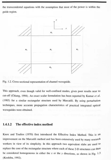
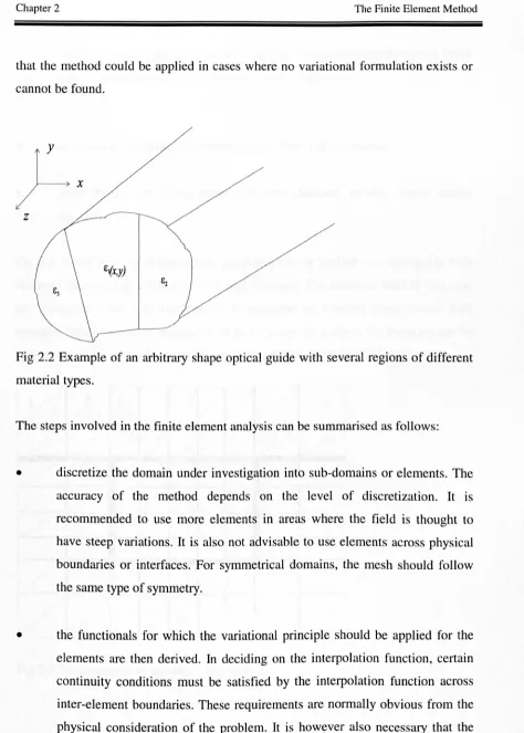
Example of an arbitrary shape optical guide with several regions of different material types
Fig 2.3 Discretization of an optical waveguide
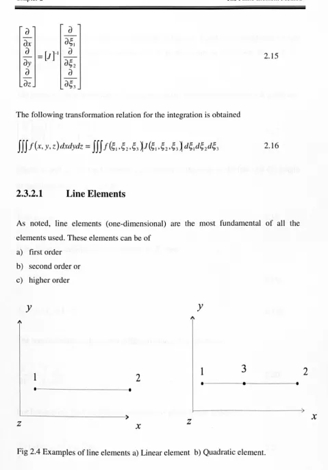
Fig 2.4 Examples of line elements a) Linear element b) Quadratic element. Fig 2.5 Triangular elements a) First order b) second order.
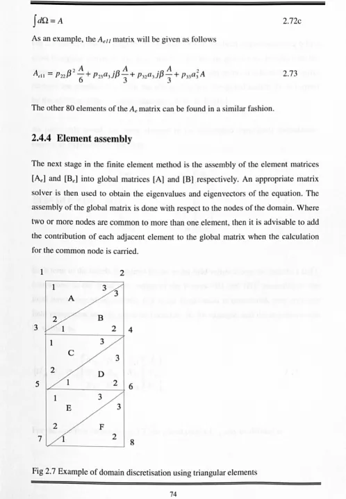
Fig 2.6 Diagram of a typical element Fig 2.7
Fig 2.8
Fig 3.1
Fig 4.1
Fig 4.2
Example of domain discretisation using triangular elements Showing the use of infinite elements at the guide boundary.
Angle Phase matching in KDP
Showing the general schematic of the waveguide under consideration The variation of the normalised propagation constant with the normalised waveguide dimension for a gaussian-gaussian diffused waveguide.
Fig 4.3 The effect of guide structure on dispersion characteristics of a
gaussian-gaussian diffused channel waveguide for two quasi-TE modes
Fig 4.4 Dispersion characteristics of a rotated y-cut LiNb03 waveguide with Gaussian index in the x-direction and various index profiles in the y-direction Fig 4.5 Dispersion characteristics of a diffused anisotropic waveguide with optical axis at 90°
Fig 4.6 The relative strength and orientation of the H field for anisotropic
waveguide with optical axis at 45°
Fig 4.7 Dispersion characteristics of the first two modes of a diffused anisotropic
waveguide with optical axis at 45°
Fig 4.8 Showing the effect of the imposition of symmetry condition on the
effective index of the first two modes of the guide
Fig 4.9 Variation of the effective index with the optical axis angle, for the ordinary mode
extraordinary mode
Fig 4.11 Diagrammatic representation of a directional coupler
Fig 5.1 Fig 5.2 Fig 5.3a Fig 5.3b Fig 5.3c Fig 5.3d Fig 5.3e Fig 5.4
all three cases Fig 5.5 matching Fig 5.6 Fig 5.7 Fig 5.8 Fig 5.9a 1.S,...,m Fig 5.9b of 1.S,...,m Fig 5.10a 3.82,um Fig 5.10b
of 3.82,um
Fig 5.11 of3.82,um Fig 5.12 4.77,um Fig 5.13 Fig 5.14
Schematic representation of the Cherenkov scheme in planar waveguide
Profile of the input field
Radiated second harmonic field at Z=1O.6,um
Radiated second harmonic field at Z=lS.9,um Radiated second harmonic field at Z=26.SJ.1m Radiated second harmonic field at Z=30.6,um Radiated second harmonic field at Z=47. 7 J.1m
Second harmonic power as a linear function of propagation distance for
Second harmonic generation in planar waveguide without quasi phase
Generated second harmonic with and without modulation QPM second harmonic generation in LiNb03
Input field profile
A two dimensional plot of the radiated SH after a propagation distance of
A three dimensional plot of the field profile after a propagation distance
A two dimensional plot of the field penetration after a propagation of
A three dimensional plot of the field profile after a propagation distance
A three dimensional plot of the field profile after a propagation distance
A two-dimensional plot of the field profile after a propagation distance of
The second harmonic power as a linear function of propagation distance Non QPM second harmonic generation in channel waveguide
coherence length of propagation.
Fig 5.15b A three-dimensional representation of the propagating field after one coherence length of propagation
Fig 5.16 Demonstrating the effect of QPM
Fig 6.1
Fig 6.2
Dependence of refractive index on fractional aluminium concentration Modelling of loss in a GaAs waveguide a) Loss coefficient as a function of propagation distance b) Loss factor as a function of propagation distance.
Fig 6.3 Modelling of loss in a AlGaAs waveguide a) Loss coefficient as a function of propagation distance b) Loss factor as a function of propagation distance
Fig 6.4 Diagrammatic representation of a waveguide structure with confinement of the fundamental wave
Fig 6.S Diagrammatic representation of a waveguide structure with confinement of the second harmonic wave
Fig 6.6
Fig 6.7 concentration
Fig 6.8
Dependence of SH output power on guide dimensions
SH power, Overlap integral and spot size as a function of aluminium
SHG in lossless AlGaAs , the variation of output power, spot size and overlap with propagation distance
Fig 6.9 lllustration of two schemes by which output power could be increased: scheme B shows domain destruction, and scheme C shows domain reversal
Fig 6.10
Fig 6.11
Comparison of SHG efficiency in QPM GaAs and AIGaAs devices Showing the effect of fabrication error on QPM
Fig 6.12 Effect of fabrication error on second harmonic output power, a comparison of idealised QPM with assumed error
Fig 6.13 A more detailed picture of domain mismatch for a -1 % error.
Fig 6.14 The effect of loss on SHG in GaAs with and without QPM
Fig 6.15 The effect of loss on second harmonic power in AIGaAs without QPM
Fig 6.16 A comparison of second harmonic output power in a loss less QPM AIGaAs device with second harmonic power in a lossy QPM AIGaAs device
Fig 6.17 A comparison of QPM second harmonic output power in lossy GaAs and AIGaAs devices
GaAs device and b) QPM GaAs device
Fig 6.19 The effect of increased input power on efficiency of generated power
Fig 6.20
errors
Fig 7.1
Fig 7.2
The variation of efficiency with input power for different fabrication
Diagrammatic representation of rib waveguide used in the simulations
Showing the transfer of power from the fundamental to the generated
second harmonic in an idealised waveguide
Fig 7.3a Fundamental field at a propagation distance of 12,um
Fig 7.3b Second harmonic field at a propagation distance of 12,um
Fig 7.3c
Fig 7.3d
Fig 7.3e
Fig 7.3f
Fig 7.4
Fig 7.5
Fig 7.6
Fig 7.7 fundamental
Fig 7.8
Fig 7.9
Fig 7.10
Fundamental field at a propagation distance of 75,um
Second harmonic field at a propagation distance of 75,um
Fundamental field at a propagation distance of 400,um
Second harmonic field at a propagation distance of 400,um
Comparing the efficiency of output for two different input power
Dependence of second harmonic power on input power
Generation of SH power with depletion in the fundamental
Showing the process of quasi phase matching with depletion in the
Effect of increased power of the second harmonic process
Showing the effect of further increase in input power
Shows the independence of two waves within the waveguide
To the many people who in diverse ways had contributed to the successful completion of this project I would like to say thank you. It is impossible to mention everyone by name without having to write another volume. However I would particularly like to thank Prof. Rahman and Prof. Grattan for their support, guidance and encouragement. Without them this whole project would have been still born. Their painstaking effort to proof read the whole of the thesis is very much appreciated. There is very little more one could
have asked from a supervisor. Prof. Rahman freely gave of his time. Always there and
patient, explaining things into minute detail. Prof. Grattan never ceased to remind me to dot my 'i's and to cross my 'Cs. To them I would like to say a big THANK YOU.
To my colleagues in the Photonics research group, Femi, Najm, Raj, Moo, Patrick, Chris, Niranthi and others I would also like to say thank you for the wonderful companionship. I am glad you were not 'worried but only wondering'. You were great guys to work with.
To my numerous friends and acquaintances I would also like to say thank you all. Here truly it is impossible to mention names otherwise this acknowledgement would become a litany of names. To the members of the Santrokofi Union-UK, my colleagues at
NewVic, I say Thank you all.
Finally but not the least I would like to thank, my grandmother, Anastasia Oyintey of ever loving memory, my mother Philomena Apietu (Akua Martha), my uncle Mgr. Rudolph Apietu (Kwaku Apietu) and my sister Mary Theodora (Wiwi), for their loving care from infancy unto this day. These were the people who watched over my first
faltering steps and have guided me through life. To these wonderful people I say 'Bilafe
ku asaa orbla, bie bla fuee'. To all other members of my immediate family I would also like to say thank you.
The University Librarian is hereby granted powers of discretion to allow this thesis to be copied in whole or in part without further reference to the author. This permission applies to only single copies made for the purposes of study and subject to the normal conditions of acknowledgement.
At the heart of future communication systems will be integrated, all optical devices. The role of the second order non linear process in the realisation of such devices is well known and has been documented. Research activity in the field of second order nonlinear processes has focused primarily on the generation of new frequencies, which have an important role to play in multimedia systems. The second order process also has great potential for use in all-optical switches, all-optical transistor and intensity-dependent phase modulation. For the theoretical study of such devices, efficient mathematical models are required. The finite element method has established itself as an accurate, efficient and versatile method in the modal analysis of both linear and nonlinear systems but its application to the evolutionary analysis has been minimal.
The application of the finite element method to the theoretical study of such devices is the subject of this thesis. A formulation of the finite element method that takes into consideration material anisotropy and different diffusion profiles is developed, as is a finite element based beam propagation model. Such a model combines the strengths of the finite element method with the weB-established beam propagation method for the evolutionary analysis of the fundamental wave and the generated second harmonic wave. The model is applied to the study of second harmonic generation in various material systems and waveguide structures.
The propagation model developed has been applied to the study of second harmonic generation in both LiNb03 and semiconductor waveguides. Second harmonic generation in waveguides with one-dimensional confinement is first studied and provides a basis for comparative analysis with previously published results. The method is then extended to more realistic guides with two-dimensional confinement. Second harmonic generation by the Cerenkov radiation scheme is illustrated. Quasi-phase matching schemes for enhancing the output power are also discussed. Semiconductor material systems provide the basis for the monolithic integration of optical waveguides and hence are of great technological importance. The method developed is thus applied to the study of SHG in GaAs and AIGaAs devices. Methods of QPM and fabrication tolerances on output power as well as waveguide loss are treated. Finally the phenomenon of cascaded second harmonic generation is considered.
As a first task, it was necessary to determine the modes or characteristic solutions of the waveguide structure through the solution of the stationary wave equation. The finite element vector H formulation was thus extended to the study of 3-D waveguides with material anisotropy and diffused index profiles, both the transverse directions. Some new and interesting observations were made. The solution obtained from the above is then used at the second stage, an input for the BPM. A step by step solution of the paraxial wave equation in the propagation direction then produces a second harmonic output. Various types of waveguides are analysed and the results fully discussed.
A TM Asynchronous Mode Transfer CW EDFA FTTH 10 ISDN OIDA PlC WDM TE TM FEM FDM BPM SHG MOCVD QPM /j.z IT Continuous Wave
Erbium-doped Fiber Amplifiers Fiber to the Home
Integrated Optics
Integrated Services Digital Network
Optoelectronics Industry Development Association
Photonics Integrated Circuits
Wavelength Division Multiplexing
Transverse Electric
Transverse Magnetic
Finite Element Method
Finite Difference Method
Beam Propagation Method
Second Harmonic Generation
Metal Organic Chemical Vapour Deposition
Quasi Phase Matching
Coherence length Attenuation constant
Propagation constant
Nonlinear susceptibility constant Step size in the propagation direction Permittivity
pi == 3.14159265
Discretization domain
Wavelength in pm
Permeabil i ty
Angular frequency
Chapter One
Introduction to Optical Waveguide Theory
1.1
Overview of research and development in lightwave technology
Optics is concerned with the propagation and interactions of electromagnetic waves with
matter. The study of light has extended the range of human vision. It enabled man to be
made aware of the existence of phenomena far beyond the range of normal human
. vision. The nature of the wave phenomenon itself and of the medium that was postulated
to support them remained a mystery until Maxwell considered the properties of
electromagnetic waves. The recognition that light is an electromagnetic wave was one of
the great milestones of scientific thought. It unified the description of a great diversity of
phenomena, and also enabled predictions to be made about previously unknown
phenomena. As a natural occurrence, light has been used by man since time immemorial:
however, as a means of communication, it was first used when man learnt how to make
fire.
Tremendous advances have since been made, particularly after the establishment of the
electromagnetic theory of light. Maxwell's electromagnetic theory of light helped to
bring into one body some of the diverse aspects of light, and arguably could be said to be
modern communications technology. Heinrich Hertz demonstrated long radio waves in 1888 and in 1895 Guglielmo Marconi demonstrated wireless communication. Since
these pioneering research works, the move has been towards obtaining more powerful communication systems using higher carrier frequencies. The range of applications has
also greatly diversified, from early voice communication systems, requiring a bandwidth
of 15kHz to analogue television with a bandwidth of 6MHz, through to microwaves for
radar applications with frequencies measured in Gigahertz. Optical frequencies are
important for of present-day systems, involving optical communications, for example
optical switches, optical storage systems and optical computing.
The invention of the laser has given a major boost to the field of optical systems. The first laser operating at a wavelength of 694nm represented an optical frequency of 5x I 014
Hz. Since the demonstration of this, the ruby laser, the transmission and processing of
optical signals has been of the greatest interest to scientists. The exploitation of the tremendous potential bandwidth offered by laser light has been potentially limited by a
number of factors:
a) It was discovered quite early that free space propagation of the laser beam was not a suitable means of establishing effective communications links. Laser light is strongly scattered by rain, fog, smog and snow. There was also the need for a
line-of-sight link, and hence the work turned to establishing suitable transmission
media. There are, however, a number of applications where it is possible, even
desirable, to use free space transmission e.g. communication between satellites in orbit.
b) Electronic components place a limitation on the bandwidth of any optical
communication system, in that it is not yet possible to use the full potential of a
1014 _1015 Hz system.
A solution to the first of these problems was to allow light to propagate through another
medium, which protects it from atmospheric interruptions. The transmission of light by
glass (and other transparent media) by multiple internal reflections had been known and
'Photophone', that varied the intensity of light incident upon it as a function of the amplitude of speech vibrations (Kapany, 1967). The development of this idea was
however hampered by very high propagation losses. Early measurements of loss in glass of near infra red light was put at 1000dB per km, which was attributed to the impurities in glass (Kao and Hockham, 1966). This effect was confirmed by Kapron et al., (1970)
who succeeded in making pure glass with a loss of 20dB per km and opened up the way for effective fibre optics. Today's optical fibers have a loss of less than 0.2dB/km on certain spectral bands.
1.1.1
Research trends in optoelectronics
The development of low loss optical fibre has helped address the problem of suitable
transmission media for modern optoelectronic systems. Present day optical fibres have transmission rates of over two billion bits per second over hundreds of kilometres with
an error of about one per billion bits and performance figures are improving year by year. Along with the development of low loss optical fibre came the development of the
compact single mode semiconductor laser since the early I 960s (Hall et al., 1962;
Nathan et al., 1962; Quist et al., 1962). By the early 1970s semiconductor lasers were
providing continuous wave (cw) coherent sources of laser light (Alferov et al., 1970;
Hayashi et al., 1970). Improvements from the 1980s made them reliable sources for use in optical communications systems.
Optical signals transmitted using optical fibres will ultimately have to be converted into
electronic form for processing. The speed of operation of electronic components is a
major determining factor in the bandwidth of a communications system. This limitation has led to major research into a field now known as optoelectronics, replacing electronic devices with optical devices, switches, modulators, filters, transmitters, connectors and
receivers. The potential of this new field is enormous. Will the development of an optical switch eventually lead to an optical computer? That is the hope and aspiration of many workers in this field. Advances in recent times in optoelectronics have led to the
development of a wide range of optical components and devices such as directional
and many others (Tamir, 1979). These advances in optical technology have resulted in
the availability of consumer goods based on optical technology, such as laser copiers,
laser printers, barcode readers, CD players and many others.
Research in the now established field of optoelectronics has developed along the
following five main directions:
I. Optical communications systems
2. Optical storage technology
3. Waveguide devices and optoelectronic packaging technology
4. Photonic devices and materials
5. Optical sensor technology, including speciality fibers
1.1.1.1
Optical communications systems
Research in this area has been mainly in the area of telecommunications. local area
networks and optical intercommunications. Many commercial organisations are building
their research. development. and marketing programs around multimedia concepts like
Visual. Intelligent, and Personal communications systems. The potential role of
optoelectronics in the development of such systems cannot be overstated. These
technologies, which enable such multimedia systems to be developed, include
high-speed digital communications, switching, high-capacity information storage, image
processing, high-definition and flat-panel displays, new kinds of consumer electronics
and local networks.
High-speed digital transmission (10 Gbitls and beyond), and switching for
telecommunications have been major development thrusts for companies like Lucent,
Alcatel, Fujitsu. Hitachi, and NEC for nearly two decades. Transmission equipment
developed by these companies pioneered the use of single-mode fiber, high bit rates, and
long wavelengths. Some of these companies were early to commit to the Asynchronous
Two important systems recently developed have been synchronous digital hierarchy
(SDH) -10 Gbit/s trunking systems using optical amplifiers (erbium-doped fiber amplifiers or EDFAs) for amplification at 1550nm, and fiber to the home (FfTH) systems capable of a two-way ISDN (integrated services digital network) at 1310nm,
combined with one-way video at 1550nm. These systems will pave the way for
interactive broad band services for homes and small businesses, generally accepted as a
key requirement for the so-called "Information Age" revolution just now beginning.
Equipment for fiber-optic broadband systems was forecast by the end of the 20lh century
to constitute two-thirds of all optical communications equipment sales, with a total value of $12 billion; and by 2003, fiber-optic broad band equipment is forecast to constitute
three-quarters of $30 billion in total optical communications sales (OIDA 1994). (The corresponding worldwide markets for all optoelectronics, including displays and storage, are estimated at $140 billion and $230 billion, respectively, in those years.)
1.1.1.2
Optical storage technology
Optical data storage, which once appeared to be a failing technology in the marketplace, is quickly finding its way into homes and offices with the multimedia revolution. In the past, it was believed that optical storage, because of its long access times, would not be a significant threat to magnetic storage. However it has become one of the important
enabling technologies fusing together the entertainment and computing industries. Developments in optical storage technology underlie developments in multimedia
systems and it is envisaged that it will form one of the major optoelectronics technologies for this, the twenty-first century.
As in all data storage systems, optical disk systems are characterised by their storage capacity, data transfer rate, access time, and cost. The wavelength of the laser used for "read and write" operations imposes a fundamental limitation on the information storage
density and the speed of data retrieval. The storage capacity of an optical storage system
in using the storage area is the areal density (MB/sq. in.). Areal density is governed by the resolution of the media, the numerical aperture of the optics and the wavelength of the laser in the optical head used for recording and readout. The data transfer rate in an optical recording system operating at a fixed rotational speed is inversely proportional to
the laser wavelength. Research and development in the field of optical storage is typically directed at:
• Reducing the spot size using lower-wavelength light sources
• Reducing the weight of optical pickup heads using holographic
components
• Increasing rotation speeds using larger optical power lasers
• Improving the efficiency of error correction codes; and increasing the
speed of the servo systems.
The introduction of the CD format in the late 1980s, opened up another direction for optical storage devices. Due to their low-cost replication capability, high capacity,
robustness, and removability, optical CD-ROM systems have become competitive with magnetic floppy disks for applications such as software distribution and home multimedia applications. The success of CD-ROM technology in the consumer market has allowed the cost of optoelectronic components such as CD lasers to drop sharply
over the last few years, paving the way for new applications and new optical storage systems. It is expected that CD systems will remain essential for the wide commercial acceptance of optical storage systems in the years to come.
Those features which uniquely make optical storage systems attractive are their higher
capacity per disk, removability, mass replicability, and long memory persistence for
archival applications. They are most commonly used for software distribution, backup memory for personal computers and workstations, external memory for some
and possibly as a replacement for paper. New applications and markets opening to optical storage systems as their prices are dropping include home multimedia, multimedia servers, high-definition television and digital videodisks (DVD), and
massive storage systems.
1.1.1.2.1 The Data Storage Market
The growth of any data storage market is determined by various information processing
and storage applications. For the optical storage market. it is a new application,
multimedia entertainment systems. which is fuelling its growth. The volume of the data
storage market approached $100 billion as early as 1994. of which the hard disk segment
was $47 billion, the magnetic tape segment $42 billion. and the optical disk segment $6
billion.
In the past, the majority of desktop computing users did not need such a high capacity of data storage. However, during the 1993-95 period, the advent of image computing and
processing of multimedia documents with still images has quickly raised the floor of the
minimum useful desktop storage capacity to about I GB. This has made optical storage
devices more attractive. As a consequence, demand for optical storage devices exceeded supply in 1994 for the first time. With increasing demand, most optical storage
manufacturers have continued to drop prices to increase their market share. An optoelectronics Industry Development Association (OIDA) survey predicts an explosive growth in the optical storage market of $50 billion by the end of the next decade (20 I 0). It is believed that video- and computing-related products will strongly support this growth.
1.1.1.2.2
Emerging optical storage technologies
For any storage technology to remain competitive over time, it is critical that its access
time, system volume. and cost be kept constant (or preferably reduced) while its capacity and data rate are increased. This requires low-cost pickup sensors that can move quickly
that fast and accurate movements can only be achieved over short distances; this consideration leads to the conclusion that data must be kept as local as possible with
respect to the pickup heads. Historically, this consideration has driven the increase in
areal densities, allowing much larger amounts of data to be stored, accessed, and
retrieved without an increase in access time and system cost.
However, as optical areal densities approach optical diffraction limits, researchers have
started seeking new solutions. On the one hand, solutions may entail further increasing
the areal density by combating the diffraction limits of optics using, for example,
near-field optics. On the other hand, solutions may take advantage of additional available
dimensions such as are proposed for various 3-D optical storage concepts. Indeed, data
residing in a volume may be considered as being local to the pickup sensors if both the
performance cost and actual cost of accessing it in 3-D is affordable. In this case, volumetric density (Mbitlin3) becomes critical. The volumetric density is governed by the effective volume of the spot, which in turn is limited by the volumetric resolution of the medium, the numerical aperture of the optics, the wavelength, and the positional
accuracy of the pickup head in the third dimension. The spot size is limited by the recording wavelengths through diffraction effects, as well as by the sensitivity and
integration time of the readout detector. The approach promises low-cost,
high-volumetric-density ROM disk media with a thousand or more layers for image storage, and also low-cost compact disk player drive units employing semiconductor blue and/or green lasers.
The potential impact of layered 3-D optical disks on the capacity of optical storage can
be much greater than the impact of, for example, the use of blue lasers. This is because
the growth factor in capacity is directly proportional to the number of layers. Assuming
that the areal density is not affected, the 3-D layering provides the potential for realising
optical disks with capacities exceeding lOO GB, beyond the turn of the millennium. If this factor is now coupled with a reduction in spot size, then the potential storage capacity of optical storage systems will be phenomenal.
A major increase in capacity is expected over the next 3 to 5 years using lasers with
spot size. This can be expressed in terms of the wavelength (A) and the numerical
aperture (NA), of the optical system as:
. 1.8,1,
spot size =
-NA 1.1
In order to reduce the spot size, the numerical aperture may be increased, or the
wavelength may be reduced. However, since the numerical aperture also affects the
depth of focus (and the depth of focus is directly proportional to NA), increasing the
numerical aperture imposes restrictions on the media thickness and the servo controllers.
Practically, it is expected that the numerical aperture will be increased only up to 0.62
from its present value of 0.55, allowing an increase in the storage capacity of about 12%.
It is anticipated that laser wavelengths used will change over the coming years from the
present standard of 780 nm to 430 nm with the development of the low cost blue laser.
This would lead to an increase in the information storage capacity by a factor of nearly
four and also more than double the data transfer rate. Sony is actively pursuing this
direction by developing zinc-selenide-based lasers. They have currently developed such
a laser operating at room temperature, still with a relatively short lifetime. In contrast,
researchers at Nichia are actively pursuing GaN-based lasers. They have demonstrated
lasing using this material (Nakamura, 1994) and remain active in commercialising such devices. The major drawback at present of these lasers has been their extremely short
operating lifetimes but work to improve this aspect is underway. Growing GaN on a
lattice mismatch AhO) substrate is also accompanied by a large number of defects but
work is continuing to overcome these difficulties.
An alternative method of obtaining shorter wavelengths is by use of frequency-doubled
blue lasers, through the non-linear process of second harmonic generation. Several
laser-based blue-green sources are now under development and systems are commercially
available. These frequency conversion technologies rely on the availability of suitable
laser diodes, which must meet stringent requirements of high output power, single spatial
mode, spectral stability and operate within a specific range of wavelength. Efficient
fixed phase relationship. Where this is not feasible, then the direction of the spontaneous polarisation is reversed in the non-linear waveguide at regular intervals, which corresponds to the situation when the two waves are out of phase by 180°. Work in both directly generated and second harmonic devices is continuing at a rapid rate.
1.1.1.3
Guided wave devices
Another area of intensive research has been photonic devices and materials, with the emphasis on laser and optoelectronic integrated circuit technology, including both surface-emitting and edge-emitting lasers, as well as devices for use in telecommunications, sensors, and consumer products. Within the past decade, guided wave, or integrated optical (10) components in various materials have become available from a variety of vendors, world-wide and are now being deployed in commercial systems. Integrated optical devices include modulators and passive circuits in LiNbO], glass, and semiconductors; these devices are applied to telecommunications, cable television (CATV), and instrumentation.
Applications for integrated optics have historically been in niches of the analogue, digital, and sensor fiber-optic markets; at present, however, major new markets are emerging. Perhaps the largest new market is telecommunications, where 10 devices will be used for multigigabit data transmission, signal splitting and loop distribution, and bi-directional communication modules. A second new market is CATV, where 10 modules
will be used for external modulation in fiber-optic-based signal distribution systems. In
both telecommunications and CA TV, 10 devices enable signal transmission at higher data rates and over longer distances. In a third market, instrumentation, a major
application is fiber-optic gyroscopes. An early market study of 10 modulators predicted
a 24% annual growth rate in North America over the 1993 - 2003 period (Tamir 1987). A significant portion of this growth was for aerospace and military applications (e.g.,
fiber gyros). The forecast annual sale by 2003 is nearly $200 million. The photonics market enabled by 10 modulators (e.g., transmitters and gyros) is many times larger and is expected to exceed $1 billion.
Closely coupled to this work are efforts to pigtail multiple fibers, at once, to an 10 circuit (IOC). Research and development (R&D) efforts at major centres in the world are focused on large planar Iightwave circuits (PLCs), including planar erbium-doped amplifiers, components for wavelength division multiplexing (WDM), and structures for
the silicon microbench. Much of the leading research has been performed at AT&T in the United States and NTT in Japan. In the semiconductor modulator area, the major
focus is on developing devices suitable for 10 Gbitls communications. For example,
Hitachi is working on a discrete modulator and an integrated diode laser and an electroabsorption modulator is under development at AT&T in the United States and at
NTT, NEC, and Fujitsu in Japan.
Commercial IOCs (based on annealed proton-exchange waveguides in LiNb03) are
available and widely used. 10Cs are being used in telecommunications for high-speed modulation, signal splitting and switching and bi-directional communication.
LiNb03 modulators are being used in 2.5 Gbitls (OC-48) systems to enable transmission over distances of greater than 100 km without repeaters. LiNb03 modulators make it
optimised for 1.3 micron operation. Since installing new fiber is a major cost, the
externally modulated multigigabit approach is a significant cost-saver for long-haul
telecommunications operating companies. With such systems, 10 Gbitls system
operation is achieved, for example, by multiplexing four wavelength channels at 2.5
Gbitls each.
Interest in LiNb03 modulators for radio frequency (RF) link applications is being
actively pursued at many research centres. The development of hybrid integrated optical
disk pickup heads and quasi-phase-matching structures for diode laser frequency
doubling is a topic of major research interest. Work on guided wave devices in many
places is focused on linearized modulators, high-speed and high-optical-power
modulators, modulators with gain, and frequency-doubled structures all using LiNb03.
In Japan, interest in quasi-phase-matching in LiNb03 for frequency conversion is being researched at Oki for 1.5 micron applications and at Sony for frequency doubling (blue
light generation).
1.1.1.4
Photonic devices
Research In the area of photonic devices can be classified into the following major
categories: semiconductor light-emitting diodes (LEDs), lasers, semiconductor optical
amplifiers, switches, and integrated receivers.
LEDs are the light sources used for many semiconductor-based devices. The AIGaInP material system is widely used in generating highly efficient red light for the automobile
industry and in traffic light systems and also finds application in optoisolators and low data rate «50Mbitls) optical links.
Lasers have been widely used in a number of areas: transmission lasers, pumping lasers for erbium (Er)-doped fiber amplifiers and local-loop or access lasers, are used mainly in the telecommunication industry. Included in the category of transmission lasers are
photonic integrated circuits (PICs), wavelength-division multiplexed (WDM), and
devices based on InP. Analogue lasers are used mainly in the cable TV or other
subcarrier multiplexing applications, although they are finding increasing application in
satellite communications and phased-array radars. Visible, shorter-wavelength lasers are
used for optical storage, sensing, or display applications.
The use of lasers in compact optical disk players has brought about a revolution in the diode laser industry. For the first time, there has been created an application that requires the production of more than a few thousand units per month. Thus the corresponding advantages of real mass production can be employed. Rohm, a resistor manufacturing
company that expanded into lasers, perhaps best illustrates these advantages. Through the heavy use of automation (previously foreign to the laser diode business), Rohm was
able to capture half of the CD market, and in 1994 produced about 60 million laser diodes. This kind of demand has now pushed the price down to less than $1 per laser,
even with the conventional cleaved-facet technology.
Besides optical storage, major applications for lasers in the 600-800 nm range lie in optical pointers, bar-code scanners, printers, data links, and displays. The production of laser pointers relies upon visible light emission, and wavelengths in the 630-650 nm range are much better for visibility than those at approximately 670 nm, even though higher power tends to be available there. For the print heads and bar-code scanners an analogous argument holds, but here the shorter-wavelength lasers are preferable because of the sensitivity of the detecting medium. For display, again, the 670 nm is somewhat
too long.
1.2
Nonlinear effects in optics
Much of the economic potential to be realised through the application of optics in
telecommunications and information processing can be ascribed to the best use of the nonlinear effects in optics. In recent years, there has been a significant increase in the number of published papers on nonlinearity in optics, due mainly to their economic
work of several groups, e.g. Franken et al. 1961, Franken and Ward, 1963, Boyd et al., 1965, Armstrong et al., 1962, Miller, 1964.
Most material media exhibit weak nonlinearities if exposed to electromagnetic radiation
of high intensity. The discovery of many of these nonlinear effects and especially their
development however has been made possible by the invention of the laser, when the
practical applications of these effects were quickly realised. At very high intensities, the
light waves may interact with each other or with the material medium. These
nonlinearities arise from an anharmonic motion of electrons in response to the applied
field. This can lead to the observation of several effects, the most important of which can
be divided into two classes depending on their origin, be it quadratic or cubic.
If the material is regarded simplistically as a collection of charged particles, then with
the application of an electric field, an oscillation is induced in the electron cloud. At
relatively low intensities, the induced polarisation, the displacement of the electron cloud
or dipole, P is directly proportional to the magnitude of the electric field of the lightwave
P=xE
1.2where X is the linear optical susceptibility, a function of the refractive index of the
material. It is well known in physics, that the linear dependence of one physical quantity
on another is almost always an approximation, and valid only over a limited range. The
most familiar example is Hooke's law of elasticity. Laser light generates very intense
fields, which give rise to nonlinear optical effects and the expression for the polarisation
can then be written as (a detailed derivation is given in Chapter 3)
1.3
1.2.1 Quadratic nonlinear effects
The second term of equation 1.3 gives the quadratic polarisation term which gives rise to
effects, which are all of the mixing (interaction of light with nonlinear dielectric) type.
This involves the generation of sum and difference frequencies, which may take a
variety of forms. These are
Second harmonic generation: This is the coalescing of two identical photons. It
represents a special case of a process more commonly known as sum frequency
generation. In this process, light waves at two different frequencies are summed to form
the output. When the applied optical field contains just one frequency, i.e. when the two
waves are equal in frequency, power or amplitude, the quadratic polarisation will contain
a static term and a term oscillating at twice the applied frequency. The polarisation
oscillating at twice the applied frequency radiates into the medium, giving rise to SHOo
The overall effect of this process can be described as follows: part of the energy of an
optical wave of frequency w propagating through a crystal is partly converted to that of
a wave at 2w.
Parametric ampLification: This is used to build a signal from a zero value. If power is
provided at the frequency W3 and the power at the frequency w2 is initially assumed to
be zero then the growth in the signal power at
w
2 = (03 - (0, . It is assumed here that(03
»
w,.
It must also be noted that the power at W, is amplified. Thus this devicegenerates an 'idler' signal at w2 and at the same time amplifying the signal at W, . In
effect, power from a 'pump' wave at (03 is transferred to waves at frequencies
w,
andW2' where W3 = W,
+
(02' Fundamentally it is similar to second harmonic generation butthe difference is in the direction of the flow of power. In this process X(l) is changed by
an amount proportional to the pump intensity.
Frequency Up-Conversion: This is used to convert a signal from a low frequency
w,
toill,
+
(1)2=
ill3. It is also another special case of sum frequency generation. From aquantum mechanical point of view, this can be thought of as the annihilation of photons
at frequencies ill, and (1)2' and the generation of a photon at (1)). This can be used in the
detection of infrared radiation by converting the frequency into the visible or near visible
part of the spectrum.
The linear electra-optic (Pockets) effect: This is the linear variation in the refractive index of a dielectric medium caused by the application of a static electric field. This is
the simplest of the mixing processes. In this, one of the frequencies is zero i.e. an optical
wave is sent through the medium in the presence of a dc electric field. The quadratic
polarisation will then contain a term proportional to the product of the optical and dc
fields, in effect being equivalent to changing X (I) by an amount proportional to the dc
field. This causes the medium to become electrically anisotropic, thus making the phase
velocity of the propagating wave dependent on the direction of the electric field vector of
the wave. This phenomenon is useful in the design of phase modulators. If the change in
phase velocity is dependent on an applied field, it then follows that phase or frequency
modulation can be achieved in the medium.
1.2.2 Cubic nonlinear polarisation effects
Cubic nonlinear effects arise from the cubic polarisation term
c
oX(3) E ) . This gives riseto third harmonic generation, quadratic electro-optic effects, two-photon absorption and
other related mixing phenomena, i.e.
The quadratic Electro-optic effect: It is the simplest case of effects arising from cubic
polarisation. This is the variation arising in the refractive index due to a quadratic term.
An optical wave propagating through a medium in the presence of direct current (dc)
field causes a change in the refractive index of the material proportional to the square of
the direct current field. This effect is also known as the Kerr effect and may be used in
Third harmonic generation: This can occur when an incident field at frequency ill
induces a polarisation at the frequency 3ill. This process is governed by the third order
nonlinear susceptibility tensor X(3). An optical field propagating through a nonlinear
medium induces a cubic polarisation, which is proportional to the third power of the
field. The refractive index is thus modulated by an amount proportional to the optical
intensity. The induced nonlinear polarisation may then generate a travelling wave at the
third harmonic frequency.
Two-photon absorption: If two intense electromagnetic waves at frequencies (01 and ill2
propagate through a medium, then there is the probability that some energy will be
absorbed from both of these waves as result of the transition at the sum frequency
illt where illt
=
ill 1+
w2 . In semiconductor materials the transition is usually between the
valence and conduction bands. This phenomenon can be used for the observation of
extremely short light pulses.
Raman effect: Given light of a particular frequency, travelling in a dielectric medium, it
is then possible to observe weak side bands of radiation close to the frequency of the
incident light. The vibrational resonant frequency of the material determines the
difference from the incident frequency of the side bands. This phenomenon is similar to
a parametric processes: however there are two main differences. The 'idler' wave will
now be replaced by an internal oscillation of the molecule, in other words a mechanical
crystal vibration instead of the electromagnetic idler wave. This phenomenon is
therefore possible only in materials whose molecules are capable of vibrational
oscillation. No phase matching is also required. The spontaneous Raman effect is used in
the spectroscopic investigation of the structure of molecules whereas the stimulated
Raman effect is used in the design and fabrication of optical amplifiers and oscillators.
1.3
Fundamental Theory underlying optical waveguide analysis
The field of integrated optics can broadly be classified into areas involving optical fiber
circuit (OIC) can be regarded as the optical equivalent of the conventional electronic
circuit, where the fundamental material that interconnects the various devices of an OIC
is the optical waveguide. Unlike electrical circuits where the signal is carried by a
current, the signal in an optical waveguide travels in distinct optical modes. A mode can
simply be regarded as the spatial distribution of optical energy in one or more
dimensions. In this section, Maxwell's equations for the propagation of waves in optical
waveguides are presented, and different types of waveguides are then reviewed.
1.3.1 Maxwell's Equations
The work presented in this thesis is based on a numerical solution of Maxwell's
equations, which govern the propagation of light through an optical medium and its
interaction with the medium. These equations are valid for the entire frequency spectrum
and in differential form can be stated as follows:
aB
VxE+-=O
at
an
VxH--=O
at
V·D=p
V·B=O
(Faraday's law) 1.4
(Maxwell-Ampere law) 1.5
(Gauss's law) 1.6
(Gauss's law magnetic) 1.7
For a lossless dielectric isotropic material, the electric E and magnetic H field vectors
are related through the constitutive equations
D=£E+P 1.8
In the above D is the electric flux density (coulombs/m2), B is the magnetic flux density
(webers/m2), p is the charge density, f..lo = 4n x LO-7 F/m is a constant equal to the
magnetic permeability of a vacuum and c" is the vacuum dielectric permitivity.
Assuming complex time dependence through the factor exp(jwt) , where j is an
imaginary unit, W the angular frequency and t is time, and substituting for Band D, the time derivatives in the above equations may be rewritten as
v
x
E + j wf..lH=
0 1.10VxH- jWcE=O
1.1 ITaking the curl of these equations and making the necessary substitution from equations (1.4) and (1.5), equations (I. 10) and (I. I I) could be written as follows
1.12
1.13
Using the following vector identity
VxVxA
=
V(V
·A)_V
2
A
1.14the first terms of equations (1.12) and (I. I 3) may be written as
1.15
1.16
1.17a
1.17b
These two equations can be written as:
1.ISa
1.ISb
where the wavenumber, k = m~£J1(1 .
The equations (1.17) or (I.IS) provide the general solution to Maxwell's equations in terms of material properties and the angular frequency of the electromagnetic signal. It i these two equations, which need to be solved for a particular waveguide structure, with
appropriate boundary conditions, in order to obtain the optical mode, in other words the
field and its characteristics.
1.3.2 Planar waveguides
Various types of optical waveguides exist, the simplest of which is the 2 dimensional
y
L
xo
t
-t
n,
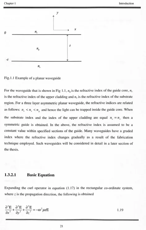
Fig.I.1 Example of a planar waveguide
For the waveguide that is shown in Fig 1.1, nli is the refractive index of the guide core, ne
is the refractive index of the upper cladding and n.l' is the refractive index of the substrate
region. For a three layer asymmetric planar waveguide, the refractive indices are related
as follows: ne < n" < nil and hence the light can be trapped inside the guide core. When
the substrate index and the index of the upper cladding are equal ne = n" then a
symmetric guide is obtained. In the above, the refractive index is assumed to be a
constant value within specified sections of the guide. Many waveguides have a graded
index where the refractive index changes gradually as a result of the fabrication
technique employed. Such waveguides will be considered in detail in a later section of
the thesis.
1.3.2.1
Basic Equation
Expanding the curl operator in equation (1.17) in the rectangular co-ordinate system,
where
z
is the propagation direction, the following is obtained [image:39.499.16.488.28.769.2]The field vector E can be separated into the individual component parts, such that there
is an equivalent differential equation for each of the vector components.
1.20a
1.20b
1.20c
1.3.2.2
Analytic solution
In a planar waveguide structure, the field quantities are assumed to vary in only one
transverse direction. Considering the three-layer waveguide structure shown in Fig. 1.1,
and assuming the light confinement to be in the y-direction, then the partial derivative
along the x-direction can be written
as~
=
O. If the parameter c/J is now defined suchdx
that
ForTE mode
ForTM mode
then equations (1.18a and b) can be written as
where n =
F,.
andf3
is the phase constant.1.21
For 2-D waveguides, the TE mode has no longitudinal component of the electric field,
Ez = 0 . The non-vanishing field components are thus defined as:
H
=L
Ey wJ.1 x 1.23
H =_l_dEx
z jwJ.1
dy
1.24
E
=
LH
+_l_dHzx W£ )' jw£
d
y
1.25
For TM modes, there is no magnetic field component along the direction of propagation,
Hz = O. The only non-vanishing field components are thus
E
=-L
Hy W£ x 1.26
E - - - -_ 1
dH
xZ jw£
dy
1.27
f3 1 dEz
H = E
-x WJ.1 )' jwJ.1
dy
1.28
The solutions to (1.22) are either exponential or sinusoidal functions of y in each of the
regions of the waveguide. The particular function is dependent on the factor
(k
,;
n
2 - f32). For the three-layered asymmetric planar waveguide, for a guided wave thephase constant f3 will satisfy the following condition kn,. ::; f3 ::; kn f . Equation (1.22)
{
AI: exp(-acY)
f/J
=
AI' cos kf Y+
B f sin kf Y A.,. exp[a.,
.
(y
+ t )]O~ Y
-l:S;y:S;O
Y ~-t
1.29
[n the above A J ' B J ' Ac and A, are arbitrary constants determined by the boundary
conditions, which must be satisfied at the interface of two media [Appendix I
J.
The values
a
c' a.,., and k J are defined as1.30
1.31
1.32
These are well-confined modes normally referred to as TEJTMo and TEIITMI modes.
For {3 > kn J ' the function f/J must be exponential in all three regions, which would imply
infinite energy in the upper and lower cladding of the waveguide (Hunsperger, 1984).
Such a mode will, of course, not exist. A substrate radiation mode is obtained for a value
of kn, > {3 > knc and this mode is confined at the interface of the upper cladding but
varies sinusoidally in the substrate. Such a mode can only be supported over short
distances as it losses energy from the guiding region to the substrate region and hence is
not very useful in signal transmission. It may, however, prove useful in tapered coupler
applications. The number of modes that can be supported by a waveguide depends on the
thickness of the waveguiding layer and on the material properties of the waveguide, as
well as on the frequency. This implies that for a given waveguide thickness and given
refractive indices, there is a cut-off frequency, Wc below which waveguiding cannot occur. In optical waveguide applications, the wavelength is of fixed value, and the
problem is therefore to determine the refractive index values for which a particular mode
. d· I d A. (2m+l)2
A
?
In Ices are re ate through til1
=
nf - n. 2: (I , (Hunsperger, 1984), where m
=
.1 32n ft2
0, I ,2 ... is the mode number, Il)s the vacuum wavelength and t is the thickness of the
waveguiding layer.
1.4
Methods of solution of optical waveguide problems
The properties of planar waveguides, useful in many applications can be studied by
means of using analytic methods. Exact analytical solutions can also be obtained for
planar guides with stepped refractive index values but for a continuously graded index
guide, it is rather difficult to obtain exact analytical solutions. Planar waveguides, useful
in many applications have a limited range of use due to their one-dimensional optical
confinement. In many applications, two-dimensional confinement is required, and this
can be provided by channel or three-dimensional waveguides. It is not possible to obtain
exact analytical solutions to such waveguides, except in very special cases, and many
practical waveguides have complex structures with arbitrary index distribution. The
propagation mode is often a hybrid mode, E;'", (the main components of the
electromagnetic field being Ex and Hy) or E;,,,, (the main components of the
electromagnetic field being Ey and Hx) modes, where the subscripts m and n refer to the mode order such that m, n
=
1,2,3 ... , corresponding to the total number of extrema appearing in distribution of the electric fields in both the x and y directions. In reality,one of the modes is dominant, TEY in the case of
E
;'m
mode and the TMY in the case ofE;'III where the existence of such modes compounds the complexity of obtaining an
analytical solution. Amongst the many other reasons why it is difficult to obtain an exact
analytical solution to Maxwell's equations are the following major factors:
a. the electromagnetic field may extend beyond the guide core
b. anisotropic materials and non-linear optical materials may be used to