271
THE BOOST CONVERTER – REVISITED
B. W. Williams, T. C. LimDepartment of Electronic and Electrical Engineering, University of Strathclyde, Glasgow G1 1XW, UK
Abstract - The dc-to-dc boost converter is a single-switch, single-inductor, switching circuit used to efficiently transform energy from one dc voltage level to a greater voltage level of the same relative polarity. For a specific resistive load range, as the duty cycle decreases, the boost converter inductor enters a discontinuous current mode of operation - the output load current having decreased to a definable level. This paper analyses the fact that a further reduction of load current, as the duty cycle decreases towards zero, will always result in the re-emergence of a continuous inductor current condition. Further, at the other load extreme, high-current, progressively for increasing load current, starting at low duty cycle conditions, the minimum inductor current always increases from a fixed normalised current level, for a specific load range. These and other hitherto unexplored boost converter properties are analysed
and verified mathematically and with PSpice
simulations.
Keywords - switched mode power supplies, smps, boost converter, dc to dc converters.
I. INTRODUCTION
A. Species Distribution Models (SDMs)
The three common non-isolated, switch, single-inductor, dc-to-dc converters (switch mode power supplies - smps) are
the forward (or buck or step-down) converter;
the step-up (or boost) converter; and
the inverting step-up/down (or buck-boost)
converter.
Each of these converters operates on the principle of taking input dc supply energy, temporarily storing that energy in the magnetic field of an inductor, then that energy is diverted to the load, which can be at a potential and polarity different to the input energy source emf voltage.
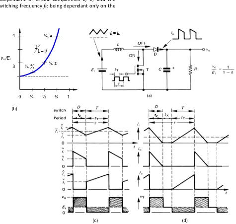
This paper is specifically concerned with the boost converter shown in figure 1a and extends the analyses and understanding of its basic traditionally
accepted operating modes and properties. The background theory is briefly presented to establish existing boost converter operational interpretation and to define the necessary concepts and parameters.
The boost converter in its basic form converters dc voltage source energy to a higher voltage level, using switch mode (hard or soft) techniques (namely, the switch is either cut-off or fully on - saturated). The boost converter is used to step up the low output voltage of PV arrays to a voltage level commensurate with inverter link voltages suitable for transformerless ac grid interfacing [1]. Because of its continuous input current characteristic the boost converter is used extensively for extracting sinusoidal current at controllable power factor from wind turbine ac generators [2].
As shown in figure 1b, operation and the output voltage are characterised by the switch on-time duty cycle δ, and analysis is centred on the inductor current iL and inductor voltage vL, as shown in figures 1c and 1d. Specifically, in steady-state, analysis is based on the inductor satisfying Faraday’s equation
L L
di
v L
dt
Steady-state theoretical analysis assumes zero switch and diode losses, an infinite output capacitance C, and zero source and inductor resistance; then the switch on-state and off-state currents created Kirchhoff loops yield
(V.s) L i T o D
L i E t v t
(1)
which after rearranging the last equality, gives the traditional boost converter voltage and current transfer function expression
1 (pu)
1 i o
i o
v I
E I
(2)
272
o o
i i
E I
v I
- termed power invariance. This
expression, equation (2), assumes continuous current in the inductor when the switch is off, during the period tD, such that tT tD , where the steady-state switching frequency is fs 1/ and the normalised switch on-period is
t
T/
.Equation (2) highlights that the relationship between
the input and output voltages (and currents) is
independent of circuit components
L,
C
, and the
switching frequency
f
s: being dependant only on the
switch on-state duty cycle
δ
, provided inductor
current flows throughout the whole switch off-state
period,
t
D, normalised as
δ
D=
t
D/
τ
=
1
-
δ
. This
inductor current condition is termed
continuous
conduction
. A continuous current requirement is
highlighted when considering the circuit energy
transfer balance between the input and the output:
2 2
½ /
1 / (W)
L L
o o
i o
L
i o
i L o
E I L i i v I
E I L I i v I
[image:2.596.57.532.214.665.2](3)
Fig .1. Non-isolated, step-up, flyback converter (boost converter) where vo ≥ Ei: (a) circuit diagram; (b) voltage transfer function dependence on duty cycle δ; (c) waveforms for continuous input (inductor) current; and (d) waveforms for discontinuous input (inductor) current.
The last term in (3) is the continuous power consumed by the load, while the second term is the energy (whence power) transferred from the inductor
to the load. The first term is the energy derived from the source Ei delivered through the inductor, while the inductor is also transferring energy to the load (when ii = iL
tD tD
4
3
2
1
0
0 ¼ ½ ¾ 1
δ vo /Ei
½, 2 ¾, 4
(c) (d)
(b)
1 1
273
the switch is off). A similar energy transfer mechanism occurs with the step-up ac auto-transformer. In using the factor 1 - δ in equation (3), it is assumed that energy is transferred to the load from the supply, during the whole period the switch is off, that is, continuous inductor current. Since the inductor is in series with the input, the input current terms are interchangeable with the corresponding inductor current terms, for example, Assuming power from the emf source Ei is equal to power delivered to the load, power invariance, then equation (3) reduces to equation (2), or in a rearranged form
(V) i o o
E v v
(4)
In this form, it can be seen that the output voltage vo has a component due the input dc supply Ei, and a boost component proportional to the switch on-state duty cycle δ, illustrating that the output voltage magnitude vo is equal to or greater than the input voltage (emf) magnitude Ei.
Traditional theory considers when the load energy
requirement falls below that level necessitating the
inductor carry current during the whole period when
the switch is off: termed
discontinuous inductor
current
. Three sequential cycle stages (rather than
two) now occur during the interval
τ:
the period when the switch conducts, tT, normalised as
t
T/
the period when the inductor and diode conduct, tD, normalised as
D t
D/
the period tx is when the inductor and diode cease to conduct before t= τ; normalised as
x t
x/
such that tT +tD +tx =τ or when normalised δ+δD +δx =1, as shown in figure 1d.
From equation (1), using
L i T i
E t
E
i
L
L
(5)
where iL 0 when the switch is turned on then
½ L ½ i
L o
E
I
I
i
L
Assuming power invariance and substituting
I
L I
i( o 1) ½ i o
i
v
E
I
E
L
that is, after various
E I
i i v I
o osubstitutions: 22
2
1
1 1
2 2 1
2
o i o
i o i i
i
v E v
E L I L I E
L I
(6)
Note that power invariance is valid for all inductor current conditions, namely, both continuous and
discontinuous currents – during steady-state
operation. But equation (6) is only valid for discontinuous inductor current, and its boundary with continuous inductor current operation. Equation (6) is consistent with power invariance, where, for discontinuous current, equation (3) becomes
½ L2/
o o
o i
v I
E I
L i
(7)
Operational interest centres on the boundary conditions between continuous and discontinuous inductor current, where the basic voltage and current transfer function in (2) remains valid. On the verge of continuous conduction, any of the equations in (6) rearranged give the boundary critical output current
(1 ) 2i
o critical
E
I
L
(8)
Using
v
o I R
o and equation (2), the critical boundary load resistance Rcritical is given by
2
2 2
Ω 1
1
o o
critical
o critical i
v L v L
R
I E
(9)
A fact not previously specifically stated in the literature, is that the last equality in this critical resistance expression is common to all three single-inductor, single-switch smps (buck, boost and buck-boost):
21
ocritical i
v L
R
E
(10)
274
27 2
critical L R
(11)
when δ=⅓ and vo = 1.5×Ei, which corresponds to a maximum critical current of
4 (A)
2 27
o o
o critical
critical
v v
I
L
R
(12)
At other output voltages, when δ≠⅓, lower currents (larger load resistance,
R
critical) can be tolerated before the onset of discontinuous inductor current. Alternatively, equation (13) shows that critical resistance is inversely proportional to inductor ripple current. That is, a large continuous inductor ripple current and low duty cycle undesirably enhance the early onset of inductor discontinuous ripple current.
2 2 1i critical
L
E
R
i
(13)
II. INDUCTOR ONTINUOUS/DISCONTINUOUS CURRENT BOUNDARY OPERATIONAL
ANALYSIS METHODS
The expressions in equation (6) are only valid for discontinuous inductor current, and on the boundary with continuous conduction, since their derivation is based on iL 0.
Two methods are commonly employed to analyse discontinuous current conduction operation, equation (6), namely:
The voltage transfer function is normalised with respect to
the maximum discontinuous inductor current in terms of the input current
I
i the maximum discontinuous inductor current in terms of the output current
I
owhere in each case the input voltage
E
i and output voltagev
o are, in turn, assumed constant.The voltage transfer function is normalised in terms of the load resistance. This involves the smps time constant L/R, (formed by the circuit when the switch is off), being normalised by the reciprocal of the
switching frequency, namely, τ.
A. Normalisation in terms of the maximum discontinuous inductor current
Of the four possible I-V combinations that can be analysed, the case specifically considered here, by way of example, is when the output voltage vo is assumed constant (as opposed to the input voltage, Ei) and is normalised with respect to the output current, Io (as opposed to the input current, Ii). This
specific case (
v
o I
o, effectively load resistance) is considered since it later represents the situation which best presents hitherto unexplored properties. Consider equation (6), specifically2 1
2
o i
i o
v
E
E
L I
(14)
which gives
2
1 /
2
o o
o
i o
i
v
v
v
E
LI
E
(15)
At maximum discontinuous inductor current (at the boundary between continuous and discontinuous inductor current), the transfer function, equation (2) is valid, and on substitution into equation (15) gives a cubic polynomial in δ
2 1 2o o
v
I
L
(16)
The maximum average output current on the boundary, for a constant output voltage vo, is found by differentiating (16) with respect to duty cycle δ, and equating to zero. On substituting the conditional result δ=⅓, this yields (as in equation (12))
1
3
when and
4
1½
2 27
o o
o
i
v v
I
L E
(17)
275
2constant
½ ½ 1 27 /
o
o o
i v
o
v I
E I
(18)
The boundary equation between continuous and discontinuous inductor current conduction, relating the output current and duty cycle can be found by substituting the transfer function 1/1
, which is valid on the boundary, into (18), which yields
2 274 1
critical o
critical o
R
I
R
I
(19)
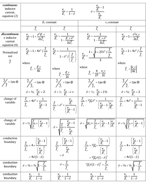
Equations (14) to (19) are presented in the penultimate column of Table 1, where the results of similar analysis for the other normalised input and output voltage and current conditions, being established background, are also summarised. The table also shows rearranged boundary conditions for each variable ( ,
v
o/E
i, andI
o/I
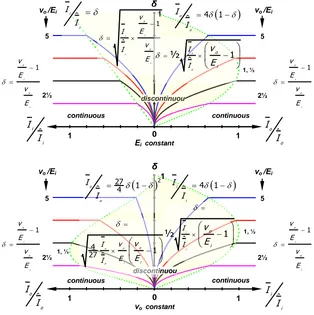
o), in terms of the other variables, as in equation (19), for example. These normalised equations and their various rearranged forms are plotted in figures 2, 3, and 4. Each figure has four different plots, one for each of the possible normalised input and output voltage and current combination.i.
versus /I I
- figure 2
[3]
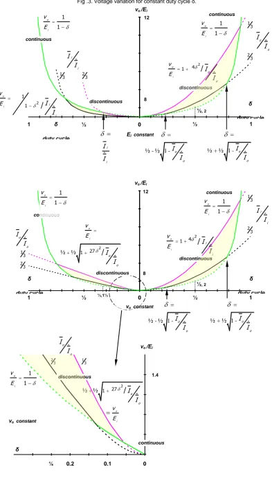
Figure 2 shows how, to maintain a constant output voltage, the duty cycle must decrease as the load voltage tends to increase once the discontinuous conduction region is entered. As would be expected, independent of which input or output parameter is controlled, discontinuous inductor current results in over charging the output capacitor, thus the duty cycle must be decreased to reduce the energy transferred to the load, so as to maintain the required constant output voltage. Figure 2c shows the normalised condition as per equation (17), namely a peak boundary condition of δ =⅓ at vo = 1.5×Ei. Because of power invariance, the two plots on the right in figure 2, have the identical shape, with variables interchanged appropriately.
ii.
o versus /i
v
E I I
- figure 3
[3], [4]
Figure 3 conveys similar information to figure 2.
However, figure 3 shows the more practical situation of how, for an increasing load resistance, for a given fixed duty cycle δ, the output voltage increases, when the load (hence input) current decreases once
entering the discontinuous conduction region.
Because of power invariance, the two right hand plots have the same shape. The four plots in figure 3 predict an infinite output voltage, but a finite output current as the load current decreases: for a constant duty cycle, discontinuous inductor current occurs for all currents below the critical level.
iii.
o versusi
v
[image:5.596.56.221.66.105.2]E
- figure 4
Figure 4 affords a more informative representation of the various circuit equations. Each of the four parts of figure 4 show voltage transfer function variation with duty cycle. Each plot therefore involves the basic voltage transfer ratio curve, in the continuous current region:
1 1 o
i
v
E
The main region of concern is when the normalised current variable is less than one, in other words, when there is a possibility of discontinuous inductor current. By way of example, each graph has plotted two normalised currents of less than one, namely
1 2
3 and .3 /
I I
Both of these load currentconditions introduce a region where the transfer
function becomes load current dependent –
discontinuous inductor current.
In the case where the input voltage Ei is constant, for loads based on the input current, the duty cycle boundary between the two modes occurs at
2
where 1 for
1 /
i
i
o i
i i
i
i I
I
v I
E I
I I
[image:5.596.309.480.587.677.2]276
2
where
½ ½ 1
-1 4 /
o
o
o i
i i
I I
v I
E I
between the two duty cycle boundary points. Again, because of power invariance this plot is the same as when the output voltage is constant, for varying input current conditions.
The remaining plot in figure 4 and its insert, is most important since it represents the mode where the output conditions are controlled, as is the usual method of using the boost converter. A region of discontinuous inductor current occurs, for duty cycle values above and below which operation returns to continuous conduction [5]. The two boundary conditions for 0 1 are two of the roots of the cubic (see Appendix for the general expressions for roots of this cubic)
27 4
2
1
I
oI
o
(20)
and the corresponding voltage transfer function is as shown in Table 2. From Table 1 the voltage transfer function is
½ 1 1 27 2/
o o
i
v I
E
I
o
The voltage transfer function for discontinuous inductor current is approximately linear with duty cycle over a wide range:
3 3 2
½ /
o
o i
v
I
E
I
o
The plot shows that discontinuity commences at
1
3 with o 1½when o 1 i
v I
E
Io
Another rational boundary solution is
2
3 2
3 and 2 - 3 with o 3when o ½
i
o
v I
E I
In all four cases (input/output I-V), the boundary conditions correspond to the appropriate vertical line
0
I I
/ 1 boundary intersection points on theplots in figures 2 and 3.The properties of the cubic polynomial in equation (20) bare closer examination.From the Appendix, three real roots exist
(discontinuous current conditions) if
/ / 1 0
o o o o
I
I
I
I
which is true for 0
I
o /I
o 1 - the discontinuous inductor current condition. The exact roots of equation (20) in terms of the coefficients of the cubic are given in the Appendix.The voltage transfer function can be expressed in terms of the duty cycle at the boundary of continuous inductor current. That is, from Table 1 – the third formula column, for vo constant and the output current normalised
2 327 27
4 4
1
1 o
i o
o o
i v E I
v I
E
(21)
Factorising the last equality, which produces a cubic polynomial, yields
1 o/ i 1 1 o/ i 2 o/ i 1 0
v v v
E E E
(22)
The first root confirms that the boundary for discontinuous conduction is
1 /
1
o i v
E
(23)
277
Table 1. Step-up converter transfer functions with constant input voltage, Ei, and constant output voltage, vo, with respect to Ioand Iicontinuous
inductor
current,
equation (2)
1 1 o iv
E
1 o i o i v E v E
E
iconstant
v
oconstant
I
oI
iI
oI
idiscontinuou
s
inductor
current
equation (6)
2 1 2 o i i ov
E
E
LI
2
1 1 2 o i i i v E E LI 2 1 1 2 o i i i v E E LI 2 1 2 o o i i
v
v
E
LI
Normalised
wrt
I
21 4 /
o o
i
v
I
E
I
o
where
8
i E Io L
2 1 1 / o i i v E I I
i
where
2i
E
I
L
i
2
1 1 27 /
2 o o i
I
v
I
E
owhere
4 27 2ov
I
o L
2
1 4 /
o i
i
v
I
E
I
i
where
8
o v Ii L
1pu@
I
I 1pu@
o
o
I
I
δ
= ½;
o 2 iv
E
1pu@ i iI
I
δ
= 1;
o iv
E
1pu@ o o
I
I
δ
= ⅓;
o 1½ iv
E
1pu@ i iI
I
δ
= ½;
o 2 iv
E
change of
variable
2 1 4 1 o o o iI
v
I
E
2 1 o i i o i v E I v I E i 2 27 4 1 1 o o o o i i I v v I E E 2 1 4 1 i o i iI
v
I
E
change of
variable
½ o o 1i v I E I o 1 o i i o i v I E v I E i 4 27 1 o o o i i v v I E E I
o½ i o 1
i v I E I i
conduction
boundary
2 1 4 4 1 o i o o o i v E I v I E 1 o i i o i v E I v I E i
3 2 27 4 27 4 1 1 o i o o o i v E I v I E
2 1 4 4 1 o i i o i i v E I v I E conduction
boundary
½ ½ 1 oo I I i I I i
27 4 21
I
oI
o
½ ½ 1 i
i I I
conduction
boundary
1 1 o iv
E
1 1 o
i
v
E
1 1 o
i
v
E
1 1 o
i
v
278
5 2½ 1⅔ 1¼ 5 2½ 1⅔ 1¼vo /Ei
vo /Ei
1, ⅓ 1, ½ δ 1 1 1 0 continuous continuous
vo constant
discontinuou s
o o
I
I i i
I I
227
4 1
o
o
I
I
4
27 o o 1
i o o i v I E I v E 1 o i o i v E v E 1 o i o i v E v E
4 1 i i II
1 ½ i i o i I I v E
vo /Ei
vo /Ei
1, ½ δ 1 0 1 1 continuous continuous
Ei constant
discontinuou s o o I I i i I I i i I
I o 1
i i o i i v E I v I E 1 o i o i v E v E 1 o i o i v E v E
4 1 o o II
[image:8.596.142.456.87.402.2]5 2½ 1⅔ 1¼ 5 2½ 1⅔ 1¼ 1 ½ o o o i I I v E
Fig .2. Control of duty cycle δ to maintain a constant output voltage.
o o
I
I i i
I I 1 1 o i v
E
2 1 4 o i o i v E v E 3 27 4 1 o i o i v E v E 2 4 1 o i i i v E I I 2 27 4 1 o o i i v v E E 1 1 o i v
E 1½ 1,
δ=⅓
δ=½
δ=¼ 3 2½ 2 1, 2 1 1 0 continuous continuous
vo constant
vo /Ei
discontinuou s
0 0
0 0
δ=½
δ=¼
vo /Ei
0 1
1
continuous continuous
δ2
Ei constant
discontinuou s 3 2½ 2 1½ 1
1 0 0
1, 2 δ=½
δ=¼ δ=½
δ=¼
o o I I i i I I 1 o i o i v E v E 2 1 4 o i o i v E v E 2 1 o i o i v E v E 1 1 o i v
E
1 1
o
i
v E
279
[image:9.596.100.494.66.757.2]Fig .3. Voltage variation for constant duty cycle δ.
Fig .4. Output voltage variation for constant current.
vo /Ei
0 1
1 continuous
continuous
Ei constant
discontinuous
12
8
4
2
½, 2 discontinuous
½ ½
δ duty cycle δ
duty cycle
1 1
o
i
v
E 13
2 3
o o
I I
1 2
3 3
i
i
I I
1 1
o
i
v
E
2
4
1 /
o
i
o o
v
E I I
2
1
1 /
o
i i
i
v
E I
I
i
i
I I
½ + ½ 1 - o
o
I I
½ - ½ 1 - o
o
I I
2 1
3 3
o o
I I
1 1
o
i
v
E
½ ½ 1 27 2/
o
i o
o
v E
I I
vo constant
vo /Ei
0
1.4
1.2
0.1 0.2
¼
δ
duty cycle
continuous discontinuous
⅓,1½
1
1 0
continuous
continuous
vo constant
vo /Ei
discontinuous
discontinuous
½ ½
12
8
4
2
½, 2
δ duty cycle δ
duty cycle 1
3 2
3 o
o
I I
1 1
o
i
v
E
1 1
o
i
v
E 13
2 3
i
i
I I
2
4
1 /
o
i
i
i
v
E I
I
½ ½ 1 27 2/
o
i
o o
v E
I I
½ + ½ 1 - o
o
I I
½ - ½ 1 - o
o
I I
280
B. Normalisation in terms of load resistance
In the previous analysis, the transfer function for discontinuous conduction (and its boundary) is
normalised with respect to the maximum
discontinuous current of the form:
o o
v
I
L
(24)
Multiplying both sides by the load resistance gives
o o o
R
I R
v
k v
L
(25)
where
27
2/ o 2 (p.u.)
o
I
I
R
k Q
L
(26)
which is the ratio of two time constants – the switch off-period circuit time constant
L R
/ and the reciprocal of the switching frequency, namely,
. Being relate to circuit Q, the symbol k in (26) is the ratio of energy delivered divided by total energy stored per cycle – a characteristic not previously observed. Discontinuous inductor current [5]:
The peak inductor current iL, during discontinuous inductor current operation is determined solely by the duty cycle, according to equation (5). That is
i L
i i
E
R
R
i
k
E
E
L
The average inductor current for discontinuous inductor conduction is shown in Table 2.
Consider the central identity expression in equation (6), which assumes
i
L 02 1
2
o i
i o
v
E
E
L I
(27)
which is based on the energy equation (7) 2
½ /
o o
o i L
v I
E I
L i
On substitution of k into equation (27), after suitable multiplication by R, then vo =IoR, gives (see equation (6))
2 2 2
2
1 1 1 1 ½
2
2 2
o i i i i
i o o o o
v E E R E R k E
E L I L I R Lv v
(28)
Isolating the voltage transfer function, gives for discontinuous conduction
2
½ 1 1 2
i o
o o
i i
v
I
I
R
k
E
I
E
(29)
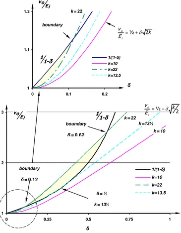
where the output current has been normalised by the minimum output current, when δ = 0, the term E Ri/ . The voltage transfer function for discontinuous inductor current in (29) along with the normal voltage transfer function in equation (2), are plotted in figure 5. The condition k = 13½, the verge of discontinuous inductor current at δ=⅓ is shown. Also shown is the boundary conditions for increased load resistance, k = 22, δ =0.62. The magnified view inset shows that continuous inductor current operation re-emerges at a low duty cycle of less than δ = 0.12. This re-emergence of continuous inductor current at low duty cycles occurs for k > 13½, and can be characterised more rigorously by investigating the minimum inductor current characteristics.
Continuous inductor current:
The key circuit parameter is the minimum inductor current,iL,
which for continuous inductor current, is given by
(A) 2
i L i
E
i
I
L
(30)
281
2
1 ½
1
L i
i i
o
i
R R R
i I
E E L
v k
E
(31)
The voltage transfer function, equations (2) and (29), various inductor currents (average IL, peak iL, minimumiL, equation (31)), etc. are summarised in Table 2. Critical circuit conditions, namely the boundary between continuous and discontinuous inductor current, occur when the minimum inductor current equals zero, that is, in equation (31) iL
equals
zero:
10 ½
1 oi
v
k
E
(32)
whence, on substituting the voltage transfer function, equation (2), which is valid on the boundary, yields
24 27 2
1 o /
o
I
k
I
(33)
[image:11.596.116.481.266.734.2]as the discontinuous current conduction boundary condition. Note the similarity to equation (19). Such analysis to derive this equation appears in texts [5], but analysis progresses little further.
Fig .5. Voltage transfer function variation with duty cycle, showing discontinuous current boundaries.
1 1.1 1.2
0 0.1 0.2
1/(1-δ) k=10 k=22 k=13.5
δ
vo Ei
k=22
1
1-δ
boundary
δ=0.12 ½ 2
o
i
v
k
E
1 2 3
0 0.25 0.5 0.75 1
1/(1-δ)
k=10 k=22
k=13.5 k=22
k=13½ k=10
δ=⅓
k=13½
vo /Ei =1½
vo Ei
δ
boundary
δ=0.62
boundary
δ=0.12
½ 2
o
i
v
k
E
282
Table 2. Step-up converter transfer functions, load resistance normalised.III. MATHEMATICALLY ANALYSIS OF THE BOUNDARY CUBIC POLYNOMIAL
Consider equation (33) rearranged into a more
general cubic polynomial form
1 2 where 2
y c c k
(34)
As a cubic polynomial, at least one real root exists
; 0 tT 1
R k L Converter Flyback-boost or step-up
discontinuous continuous
12
critical o i
k
v
k
E
2 27 2 2 1 k k 27 2k
,
io
o
i o i
v k I I R
E I E
2
½1 1 2 k
11
D D t 1 2 1 2 o i D v E
1
1 x x D t 1 -3 2 1 1 3 o i o i x k v E v E 0 , L L i iR
R
i
i
E
E
k
,0 1 ½1 o i
v
k
E
= ½ L i L L L D R I EI i i
½ 2 min 9 4 1 o i o i L i v E k v E R I E min 1 1 1 o i L i v E R I E
0 cL D o
I
i
t
I
T t t
t
t
t tT
1 o i D T v E t k t t
= ½ 1
- then otherwise 2 0, 2 2 1 1
/
T c o i o t t i T k I v k k E v t E k t t f i C ov
v
2 1 ½ 1 1 o i o o i i v k E kRC v v
E E RC ½ 1 1 o o i i
v
k
I
R
E
E
283
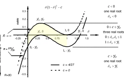
d×(1-d)² - c
-0.5 -0.4 -0.3 -0.2 -0.1 0 0.1 0.2 0.3
-0.25 0 0.25 0.5 0.75 1 1.25 1.5
d
c
u
b
ic
c = 4/27 c = 0 1
3, 0 1, 0
4 27
1,
4 27
0,
4 3, 0 1 4
3, 27
0 one real root
0
X c
4 27
4 3
one real root
X c
1 2 4
27
4 3
0
three real roots
0 , 1
1 X
c
R=0Ω
R
27L
R = 2τ
d
e
cr
ea
si
n
g
R
21 c
for
δ
. The effect of the constant term c is to produce
a Y-axis shift of the basic cubic function, thus in this
case, determining if one or more real roots exist.
The duty cycle range of interest is 0
≤
δ
≤
1 and
c
≥
0
(representing positive output current). Although
primarily interested in the roots of this cubic, those
roots are uniquely associated with the properties of
the local maxima and minima. Equating the first
differential to zero (and testing for a maxima or
minima) yields
1
3 and 1
, both independent
of
c
. The local minima
1always occurs at a value
of
-c
, the Y-axis intercept value (when
δ
=
0). The
inflexion point (second differential equated to zero)
gives
inflex 23, whence a local maxima and minima
always exist.
The local maxima and minima represent the
δ
values
at which roots emerge and disappear respectively, as
the value of
c
(the Y-axis intercept) shifts the cubic
plot up the Y-axis (decreasing current), as shown in
figure 6.
Fig .6. Boundary conditions for three real roots to the cubic equation.
Solvable, unique boundary solutions exist for δ when all three real roots exist such that two are coincident (real and equal). These cases are plotted in figure 6. Equation (34) is equated to the following general cubic with two coincident roots, which releases a solution degree of freedom.
2
21 c 0 X critical
(35)
By expanding both sides and equating coefficients, because of the released degree of freedom, a unique, viable, quadratic solution results, yielding:
1
43 or 1 and 3
critical X
and for δ =⅓, c= 4/27 (k= 13½). The root δX = supports the fact that when only one real, positive root exists, that root occurs for
X
43. Similar analysis on the local minimum yields that if only one real negative root exists that single root must be less than zero, hence a single root solution is in the range
43
[image:13.596.101.505.232.489.2]284
IV. INTERPRETATION OF THE BOOSTCONVERTER BOUNDARY CUBIC POLYNOMIAL
Interpretation of the cubic analysis results, is:
if k < 13½ (c > 4/27, with no real roots between 0 < δ < 1), discontinuous inductor current does not occur for any duty cycle δ. From equation (26), continuous inductor current results if
27 2
R
k
L
(36)
As k increases above 13½ (0 < c < 4/27), as the load resistance increases and the load current decreases,
a region about δ = ⅓ spreads asymmetrically
(towards δ = 1 and towards δ = 0), where δ in that range results in discontinuous inductor current. The implication of the critical range spreading in both directions about δ= ⅓, is significant. For a given fixed load resistance, with k > 13½, as the duty cycle decreases from a maximum, discontinuous inductor current results before δ = ⅓, but, as the duty cycle is reduced below δ=⅓, further towards zero, continuous inductor current conduction always re-emerges [5].
A corollary, at first sight contradictory, is that:
if the duty cycleδ is maintained constant as the load
current is decreased (k increased), once
discontinuous inductor current occurs, continuous inductor current operation does not re-emerge (if the duty cycle is maintained constant), as confirmed by any of the four plots in figure 3.
In figure 3 once a constant duty cycle contour enters the shaded discontinuous current region, the output voltage increases and the constant duty cycle contour remains in the discontinuous current region as the current decreases to zero. Only if the duty cycle is decreased (decreasing the energy being transferred to the load) can operation re-enter the continuous inductor current region. Theoretically continuous inductor current occurs at δ=0.
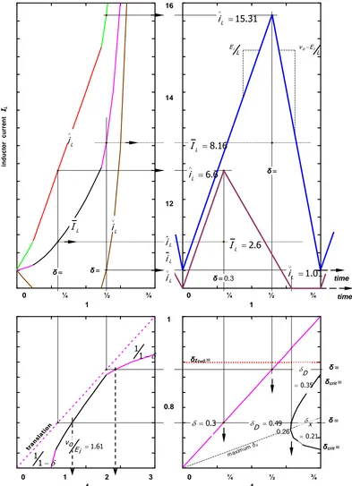
The normalised design monogram in figure 7, illustrating the equations in Table 2 with k=22, for which discontinuous conduction occurs according to equation (31), illustrates the properties of the cubic boundary equation (33). For k = 22, the boundary
values for discontinuous conduction are 0.12≤δcrit ≤ 0.62. In figure 7, the inductor current waveform is continuous for δ=0.65, then discontinuous when the duty cycle is reduced to δ=0.3. If the duty cycle is further reduced, to k=0.05, continuous conduction is predicted, as substantiated by the PSpice plots in figure 8c.
Figure 8, parts a to c, show PSpice plots for three load conditions (k=10, 13½, and 22). The first, figure 8a, is when k= 10, and continuous inductor current occurs for all δ, as predicted. The plot in figure 8b, shows operation on the verge of discontinuous conduction, when for δ=⅓ the minimum inductor current just reaches zero, as predict for k = 13½.
Figure 8c shows the case for k = 22, when
discontinuous inductor current results, but re-emerges at a lower duty cycle.
The reason why continuous current recommences at low duty cycles (δ<⅓) is related to the amount and how energy is transferred to the load. During normal operation, when the switch is off, two sources transfer energy to the load, as shown by equation (3).
2 2
½ L L /
o o
i o
E I
L i
i
v I
The source Ei energy is proportional to load current, while the energy from the inductor is quadratic current dependent, and the load current is proportional to voltage. The output voltage decreases according to 1/1 -
when inductor conduction is continuous, but is approximately proportional to duty cycle (from equation (29) and figure 5), when discontinuous. The energy from the supply when the switch is off is that necessary to maintain the output at its minimum value Ei, equation (4), while the inductor energy produces the boost voltage above Ei, δvo.285
faster rate than the inductor energy rate reduction. As
the duty cycle decreases further, the load
requirement is such to necessitate inductor energy associated with continuous inductor current. The inductor energy again balances the boost voltage according to the transfer function 1/1 -
. [image:15.596.100.493.171.714.2]Progressive a larger percentage of energy must be provided by the supply energy component, which can only support an output voltage Ei. As δ tends to zero the vast majority of the load energy is provided directly by the dc supply; with a continuous load (hence inductor) current,
I
o E R
i/ from the supply when δ= 0 and the inductor ripple current is zero.Fig .7. Step-up converter performance monogram for k = 22, giving discontinuous inductor current for 0.12 ≤ δcrit ≤ 0.62. Inductor time domain current waveforms for δcont = 0.65 (continuous inductor current) and δdis = 0.3 (discontinuous inductor current). Capacitor
discharge in switch-off period δ ≤ 0.7. tran
slat ion
0 1 2 3 4
0 ¼ ½ ¾ 1
δ= 0.65
δ= 0.3
1.61
vo Ei
1
0.8
0.6
δ
0.4
δcrit= 0.62
δcrit= 0.12
δIc=0 =
0.7
0.21 x
0.49
D
in
d
u
c
to
r
c
u
rr
e
n
t
IL
L i L
i
L
I
2.6 L
I
8.16 L
I
1.01 L
i
15.31 L
i
6.6 L
i
0 ¼ ½ ¾ 1
0 ¼ ½ ¾ 1
16
14
12
L
L
L i i
i
8
6
4
time time δ=
0.3
δ= 0.65
δ=0.3
δ= 0.65
0.26 ,
0.78
0.35 D
1
1
1
1 max
imum
δX
0.3
i E
286
V. GENERAL ANALYSIS OF THE BOOSTCONVERTER
Figure 9 shows the minimum inductor current at the boundary of discontinuous inductor current, as given by equation (31), plotted in three different domain combinations. Specifically the plots are combinations of k, δ, and the normalised minimum inductor current:
2 1½ 1
L i
R
i
k
E
(37)
Together the four shown plots reveal the underlying mechanisms of the boost converter. Reversible converter operation has been assumed in equation (37), that is the voltage transfer function, equation (2), is always valid. This recognises that if the boost converter is reversible (extra switch and diode) then the inductor current can reverse and the transfer function given by equation (2) remains valid for all δ, provided
I
o 0 with a passive R load.The first plot, 8a, of minimum inductor current versus load, k, shows the minimum inductor current reaching zero when the load resistance reaches k = 13½ for δ = ⅓, thereby confirming the solution to (35).
The minimum current locus is derived from differentiation of equation (37)
3
3 4
whence such that
2
½ 0
1
1 4
L i
k
d i R k
d E
k
Substitution of this duty cycle condition back into equation (37) gives
2
3
3 min
4 4
1 ½ 1
L i
k k
R k
i E
(38)
The straight line (equation (31)) tangents (of slope ½δ from differentiation of equation (37) with respect to k) represent the minimum inductor current variation for a constant duty cycle δ as the load k, is changed. This plot is not readily interpreted when k< 4 (high load current levels), for it tends to predict tangents such that δ< 0. Obviously δ= 0 is a restriction, hence the minimum locus plot in figure 9a is shown dashed
for
k
<
4.
The plot in figure 9b shows minimum inductor current plotted against duty cycle δ for different load conditions, k. The locus of the minimum possible inductor current for a given load is derived by differentiating equation (37) with respect to δ and equating to zero, giving
3 4 1k
which on substitution back into equation (37) yields the locus:
3min
1 3 1 L
i
R
i
E
(39)
The plot (and equation (39) when equal to zero) confirms the critical inductance current condition occurring at k = 13½ for δ = ⅓. Figure 9b sheds some light on the converter mechanisms when k < 4. As the load current increases, (that is, load resistance decreases - k decreases) the locus of minimum inductor current increases, the minimum value of which increases as duty cycle decreases. At k = 4, the minimum possible inductor current of 1 pu,
/
L i
287
k=10
o u tpu t vo ltag e (× Ei ) d u ty cycle (pu ) vo δ 1 2 3 4 5
0 τ
t
t iL
δ=¾
EI
1
¾
½
¼
δ=¾
m in im u m i n ductor cu rre n t (A) L i in duc tor vo lta ge (× Ei ) (V) vL 100 80 60 40 20 0
0 ¼ ½ ¾ 1 δ
0 τ
0 ¼ ½ ¾ 1 δ -1 0 1 2 3 4 in duc tor cu rren t (A) iL 100 80 60 40 20 0 L i
δ=0.05
1 3 δ=¾ δ=¾ δ=¾
δ=0.05
δ=0.05 1 3 1 3
vL =vo -EI
L i iL δ=0.33 iL δ=0.05
k=13½
o utput v olta ge (× Ei ) duty c y c le (p u) vo δ 1 2 3 4 5
0 τ
t
t iL
δ=¾
EI
1
¾
½
¼
δ=¾
m ini m u m i ndu c tor c urre nt (A ) L i indu c tor v o ltag e (× Ei ) (V ) vL 80 60 40 20 0
0 ¼ ½ ¾ 1 δ
0 τ
0 ¼ ½ ¾ 1 δ -1 0 1 2 3 4 indu c tor c urr ent (A ) iL 80 60 40 20 0 L i
δ=0.05
1 3 δ=¾ δ=¾ δ=¾
δ=0.05
δ=0.05 1 3 1 3
vL =vo -EI
[image:17.596.96.494.66.377.2]L i iL δ=0.33 iL δ=0.05
Fig .8a. Step-up converter performance, k=10=R. [Ei = 50V, R = 10Ω, L = 100μH, τ = 100μs, δ = 0.05, ⅓, ¾]
[image:17.596.95.497.409.718.2]288
k=22
o
utput
v
olta
ge
(×
Ei
)
duty
cy
c
le
(p
u)
vo
δ
1
2
3
4
5
0 τ
t
t iL
δ=¾
EI
1
¾
½
¼ δ=¾
m
ini
m
u
m
i
ndu
c
tor
c
urre
nt (A
)
L
i
indu
c
tor
v
o
ltag
e
(×
Ei
)
(V
)
vL
60
40
20
0
0 ¼ ½ ¾ 1 δ
0 τ
0 ¼ ½ ¾ 1 δ
-1
0
1
2
3
4
indu
c
tor
c
urr
ent
(A
)
iL
60
40
20
0
L
i
δ=0.05
1 3
δ=¾
δ=¾ δ=¾
δ=0.05
δ=0.05
1 3
1 3
vL =vo -EI
discontinuous L
i iL
δ=0.33
iL
δ=0.05
[image:18.596.97.494.77.375.2]δ=12 δ=0.62
Fig .8c. Step-up converter performance, k=22=R.[Ei = 50V, R = 10Ω, L = 100μH, τ = 100μs, δ = 0.05, ⅓, ¾]
Further insight is gained into operation below k = 4, by plot 8c which shows load resistance k plotted against duty cycle δ. The locus of minimum load resistance k for a given duty cycle is given by differentiating (37) with respect to duty cycle, when the equation is expressed in terms of k, namely
22 1
1 L i
R
k i
E
which on differentiation and equating to zero yields
3 1 3 1 Li
R
i
E
and on back substitution gives
3
min
4 1
k
k
(40)
The region of discontinuous inductor current for k > 13½ is shown shaded, and is indicated as reversible.
Notice that quadratic type minimum inductor current contours are not obtained when k < 4. The best way to interpret the region for k < 4 is to examine the extreme limit, when k = 0. In the limit, as the load resistance tends to zero, k = 0, the minimum inductor current is restricted by the duty cycle. Certain operating current and duty cycle conditions are unobtainable, as shown in plot 8d. As the minimum inductor current increases (less ripple current) the minimum necessary duty cycle increases in order to maintain the output voltage. Since the ripple current maximum peak to peak is fixed (but proportional to duty cycle), this means a limitation on the minimum ripple current at high current levels and low duty cycles. The boundary for forbidden operation in figure 9d (and also shaded in figure 9b) is given by k = 0 in equation (37), that is
2 01 1
L L
i k i
R
R
i
I
E
E
(41)
The average normalised inductor current is given when k = 0 in equation (37) or equation (41).
289
2 4 1 2 1 L i kR
i
E
(42)
Rearranging equation (41) gives the minimum duty
cycle for
k
<
4, for which the minimum normalised
inductor current is not restricted, as shown in figure
9d.
0 for 11 4
[image:19.596.43.555.68.572.2]k L i
k
R
i
E
(43)
Fig .9. Step-up converter characteristic load curves.
Maximum period Xfor zero inductor current
Figure 10 shows the boost converter characteristics for discontinuous inductor current when operating at the maximum length of time with a discontinuous current condition, X . From Table 2, the period of zero inductor current, is given by
1 -1 o i X o i v E v E 2
= ½
and o 1 1 2
i
v k
E
The maximum non-conduction period, (after
eliminating the voltage transfer function, then
differentiating and equating to zero) is when
0 1 3
-1.65 0.53 2 4
L ERi
i δ k
-1.65 0.43 22
0 13½
0.53 0.26 10
1 0 4
25 16 10 4 0 minimum locus k =Rτ/L
0 ½
1 duty cycle
δ reversible Load k
δ k
L i R E i
0.29 0 2
0.42 0 3
½ 0 4
1
2
4
6
8
0k 4
duty cycle Mi n im u m ind u c to r c u rr e n t (p .u .)
L ERi
i
forbidde
n L i 1
R E
i
minimum locus
k 4
1 3
L ERi
i
k L
i
R E i δ
4 1 0
10 0.53 0.26
13½ 0
22 -1.65 0.43 0 4 10 13 22
Mi n im u m ind u c to r c u rr e n t (p .u .) duty cycle δ 0 ½ 2 1 reve rs ib le fo rwa rd minimum locus forbidde n minimum locus
0 4 8 12 20 24 reve rs ib le fo rwa rd
δ 0 0.26 1
3
0.43
k 4 10 13½ 22
1 0.53 0
-1.65
2
1 1
3 0.43
load k Mi n im u m ind u c to r c u rr e n t (p .u .)
L ERi
i δ 0 0.26 0.43 (c) (b) (d) (a) L i R I E L i R I
E 0 4
![Fig .8a. Step-up converter performance, k=10=R. [Ei = 50V, R = 10Ω, L = 100μH, τ = 100μs, δ = 0.05, ⅓, ¾]](https://thumb-us.123doks.com/thumbv2/123dok_us/1618202.114866/17.596.95.497.409.718/fig-step-converter-performance-ei-w-mh-ms.webp)