Abstract—It is known that ripple-based control of a switching
dc-dc converter benefits from a faster transient response than a conventional PWM control switching dc-dc converter. However, ripple-based control switching dc-dc converters may suffer from fast-scale oscillation. In order to achieve fast transient response and ensure stable operation of a switching dc-dc converter over a wide load range, based on a conventional pulse train control technique, a peak capacitor current pulse train (PCC-PT) control technique is proposed in this paper. With a buck converter as an example, the operating modes, steady-state performance and transient respond performance of a PCC-PT controlled buck converter are presented and assessed. To eliminate fast-scale oscillation, circuit and control parameter design consideration are given. An accurate discrete iteration model of a PCC-PT controlled buck converter is established, based on which, the effects of circuit parameters on stability of converter operating in a DCM mode, mixed DCM-CCM mode, and CCM mode are studied. Simulation and experimental results are presented to verify the analysis results.
Index Terms— Capacitor current feedback, pulse train control, switching DC-DC converter, wide load range
I. INTRODUCTION
WITCHING DC-DC converters have been widely used in portable electronic devices, such as mobile phones, note-books and tablet PC. In some applications, the load power of switching dc-dc converters varies widely and rapidly [1-3]. Various control techniques, such as V2 control, constant-on- time (COT) control or constant-off-time (CFT) control, and pulse train (PT) control [4-10], have been reported to improve transient response speed of switching dc-dc converters. These control techniques, called ‘ripple-based control’ techniques [11], regulate the output voltage of switching DC-DC
This work was supported by the National Natural Science Foundation of China under Grant (51177140), the Fundamental Research Funds for the Central Universities under grant (2682013ZT20) and National Natural Science Foundation of China under Grant (51407054).
J. Sha, D. Xu, Y. Chen, J. Xu are with the Key Laboratory of Magnetic Suspension Technology and Maglev Vehicle, Ministry of Education, School of Electrical Engineering, Southwest Jiaotong University, Chengdu 610031, China (e-mail: [email protected]; [email protected]; chen90sky@ 163.com; [email protected]).
B. Williams is with the Department of Electronic and Electrical Engineering, Strathclyde University, Glasgow, UK (e-mail: [email protected]).
athclyde, G1 1XW, Glasgow, U.K. (e-mail: [email protected]).
converters by using output voltage ripple. Ripple-based control techniques do not require an error amplifier and its associated compensation circuit, thus, they benefit from simple control circuit design, fast transient response, and high reliability.
However, ripple-based control techniques of switching DC-DC converters usually suffer from fast-scale instability [12]. The V2 controlled buck converter has the sub-harmonic instability issue when the duty ratio D < ½ [5]. COT and CFT controlled buck converter become unstable and suffer fast-scale oscillation when the time constant of output capacitor RESRC, where RESR is equivalent series resistance (ESR) of output capacitor C, is smaller than ½τon and ½τoff (τon and τoff are on and off times of the COT and CFT control respectively) [6, 7, 10]. For a PT controlled buck converter, the ESR also significant affects control performance, with fast-scale oscillation when the ESR is small, but disappears when the ESR is large enough [13].
Studies of critical ESR have been recently reported, which provide guidelines for the design of ripple-based controlled switching DC-DC converters [4, 10, 13]. However, critical ESR is derived based on ideal conditions. The fast-scale oscillation phenomenon may still occur even when critical ESR is satisfied. In addition, larger output capacitor ESR produces larger output voltage ripple. To avoid such fast-scale oscillation, some control techniques, such as COT control with added inductor current ramp [7] and PT control with inductor current ripple injection feedback (ICRIF) [13], have been proposed. These improved control techniques combine inductor current with output voltage ripple for output voltage regulation. In this paper, based on a conventional PT control technique [14], a peak capacitor-current PT (PCC-PT) control technique is proposed. Fast-scale oscillation in the conventional PT controlled CCM buck converter is eliminated in the PCC-PT controlled buck converter. Moreover, the PCC-PT controlled buck converter benefits from simple design, fast transient response, small output voltage ripple, and a wide load range.
This paper is organized as follows. The control principle and corresponding operating modes of the PCC-PT control technique are presented in Section II. Section III addresses stability analysis of the PCC-PT controlled buck converter. The converter’s output voltage variation, output power range and line and load regulation are studied, and circuit parameter
A Peak Capacitor Current Pulse-Train
Controlled Buck Converter with Fast Transient
Response and a Wide Load Range
Jin Sha, Duo Xu, Yiming Chen, Jianping Xu and Barry W. Williams
(a)
+
–
iL L
D C
R vo
S
vp
vin
iC io
RESR
iC
Vref
+ –
Comparator
vo
D Q Q
D flip-flop
PL
PH
Control Pulse Selector Control
Pulse Generator IC,peak
Clock
Vref
t
0
vp
(n+2)T
(n+1)T
PH PL
(b)
t
vo
t
iC
0 0
nT t1
H C,peak
I L
C,peak
I
H o
v
L
o
v
H on
t toffH
L on
t
L off
t
C,n
i iC,n1
C,n 2
[image:2.612.103.240.51.260.2]i
Fig. 1. PCC-PT controlled buck converter: (a) schematic diagram and (b) time domain waveforms of PCC-PT controlled buck converter.
design consideration is presented. A discrete iteration model of the buck converter is established in Section IV. Upon this model, circuit parameter effects on stability performance of PCC-PT controlled buck converter operating in DCM mode, mixed DCM-CCM mode, and CCM mode are studied. In Section V, steady-state and transient response simulation and experimental results are presented to verify the analysis.
II. PCC-PTCONTROL TECHNIQUE
A. PCC-PT Control Technique Principle
Fig. 1 shows the schematic diagram and time domain waveforms of the PCC-PT controlled buck converter. At the start of each switching cycle, in the outer control loop, output voltage vo is sampled and compared with reference voltage Vref to determine whether high power control pulse PH or low power control pulse PL should be selected as the active control pulse in this switching cycle. As shown in Fig. 1(b), at t=nT, vo is lower than Vref, PH is selected as the active control pulse to increase the output voltage. Similarly, at t=(nT+1), vo is higher than Vref,
PL is selected as the active control pulse to decrease the output voltage.
In the inner control loop, capacitor current iC is sensed and compared with reference peak current IC, peak to determine when to turn off switch S. For buck converter, iL=iC+io, where output current io=vo/R can be considered as a constant in steady-state. Thus, the inductor current ripple flows through the output capacitor, i.e., iC is in phase with iL. At the start of a switching cycle, switch S is turned on, iC increases, and S is turned off when iC increases to IC, peak, as shown in Fig. 1(b). For high power control pulse PH, IC, peakIC, peakH , and for low power control pulse PL, IC, peakIC, peakL , that is
H
C, peak o ref C, peak L
C, peak o ref if if
I v V
I
I v V
(1)
where IC, peakH IC, peakL .
t1 t2 iL
0
iL
0
(a) (b)
nT (n+1)T nT t1 t2 (n+1)T
t1 iL
0
iL
0
(c) (d)
nT (n+1)T nT t1 (n+1)T
ton toff toff2 ton toff toff2
ton toff ton toff
IL,peak IL,peak
IL,peak IL,peak
iL,n i
L,n+1 iL,n
iL,n+1
iL,n iL,n+1i
L,n
iL,n+1
[image:2.612.347.529.54.173.2]
Fig. 2. Different inductor current modes: (a) iL, n=0 and iL, n+1=0, (b) iL, n≠0 and
iL, n+1=0, (c) iL, n=0 and iL, n+1≠0, and (d) iL, n≠0 and iL, n+1≠0.
PCC-PT control and conventional PT control have the same outer control loop [8, 9], but a different inner control loop, where PCC-PT controller utilizes capacitor current as the feedback signal to control the turn-off of pulses PH and PL.
In one switching cycle, the output voltage variation is Δvo=
vo((n+1)T)-vo(nT). According to the principle of PCC-PT control technique, control pulse PH should be applied to make the output voltage increase, that is, output voltage variation H
o
v >0. Similarly, control pulse PL should be applied to make the output voltage decrease, that is, output voltage variation L
o
v <0. PCC-PT operates in period-n states with control pulses PH and PL in n successive switching cycles constituting a controlled pulse repetition cycle, as its output voltage variation may only vary between the discrete states
H o
v
and L
o
v , rather than period-1 in the PWM switching converter [9]. Let the number of PH and PL in a control pulse repetition cycle be denoted as μH and μL respectively, then μH and μL satisfy μH/μL =voL/
H o
v
[15], and the control pulse repetition cycle period Tr is Tr = (μH+μL)T.
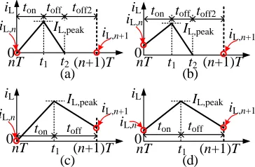
B. Operating Modes of PCC-PT Controlled Buck Converter Let iL, n and iL, n+1 denote the inductor currents at the beginning of the nth and (n+1) th switching cycle respectively. For inductor current iL of the PCC-PT controlled buck converter, there are four inductor current operation cases, as shown in Fig. 2,
Case 1: iL, n = 0 and iL, n+1 = 0, as shown in Fig. 2(a); Case 2: iL, n ≠ 0 and iL, n+1 = 0, as shown in Fig. 2(b); Case 3: iL, n = 0 and iL, n+1 ≠ 0, as shown in Fig. 2(c); Case 4: iL, n ≠ 0 and iL, n+1 ≠ 0, as shown in Fig. 2(d). Assume output voltage ripple is small enough to be ignored, that is, the output voltage can be considered as constant in a switching cycle. As iL=iC+io and io=vo/R, the peak inductor current IL, peak=IC, peak +vo/R.
If ton+toff < T, iL, n+1=0, which corresponds to Case 1 and 2, as shown in Fig. 2(a) and (b). In Cases 1 and 2, iL(t) in the nth switching cycle are
( in o)
L( ) L,n , [ , on]
v v t
i t i nT nT t
L
(2a)
o
L( ) L, peak , [ on, on off]
v
i t I t nT t nT t t
L
L( ) 0, [ on off, ( 1) ]
i t nTt t n T (2c) As iL(nT+ton) = IL, peak, from (2), the time durations ton, toff and
toff2 of the PCC-PT controlled buck converter in Fig. 2(a) and (b) can be calculated as
C, peak L, o on
in o
( / )
, n
L I i v R
t
v v
(3a) C, peak o
off
o
( / )
,
L I v R
t
v (3b)
off2 on off.
t T t t (3c) If ton and toff in Eq. (3) satisfy ton+toff >T, iL, n+1 > 0, which corresponds to Cases 3 and 4, as shown in Fig. 2(c) and (d). In Cases 3 and 4, in the nth switching cycle, i
L(t) and the time durations ton and toff should be rewritten as
in o
L( ) L,n , [ , on]
v v
i t i t nT nT t
L
(4a)
o o
L( ) ( C, peak ) , [ on, ( 1) ]
v v
i t I t nT t n T
R L
(4b)
L, C, peak o on
in o
( / )
, n
L i I v R
t
v v
(4c) off on.
t T t (4d) When ton and toff in Eq. (3) satisfy ton+toff =T, iL, n+1=0, there exists an inductor current boundary. From (3a) and (3b), such an inductor current boundary can be written as
C, peak L, o C, peak o
in o o
( / ) ( / )
0 n
L I i v R L I v R
T
v v v
(5a)
Let R in (5a) be variable, and the right part of the equation in (5a) be f(R), then
C, peak o o in
o L, o
( ) ( )
( )
0
n
f R RLI Lv Rv T v
Rv T Li v
(5b)
where f(R) = fL(R) for the low power control pulse PL, and f(R) = fH(R) for the high power control pulse PH. When f(R)<0,
iL,n+1<0; and when f(R)>0, iL, n+1>0.
Thus, in a switching cycle, when iL, n=0, f(R)<0, which
corresponding to Case 1 as shown in Fig. 2(a), means the converter operates in a DCM in this switching cycle; when iL,n≠0, f(R)>0, which corresponding to Case 4, as shown in Fig.
2(d), means the converter operates in a CCM in this switching cycle.
As the PCC-PT controlled buck converter operates in period-n states rather than period-1, that is, control pulses PH and PL in n successive switching cycles constituting a control pulse repetition cycle, rather than period-1 in a PWM switching converter [9]. In a control pulse repetition cycle, the PCC-PT controlled buck converter may operate in DCM, CCM and mixed DCM-CCM, herein mixed DCM-CCM is defined as the operating mode when both CCM and DCM exists in a control pulse repetition cycle. In mixed DCM-CCM, iL,n≠0, f(R)<0
(corresponding to Case 2 as shown in Fig. 2(b)) and iL, n=0,
f(R)>0 (corresponding to Case 3 as shown in Fig. 2(c)) may
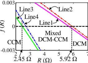
2 3 4 5 6 7
-0.003 0 0.003
R (Ω)
f
(
R
)
DCM CCM
Mixed DCM-CCM
Line1 Line2 Line3
Line4
[image:3.612.374.516.55.157.2]2.45 Ω 5.92 Ω
Fig. 3. The operating modes and corresponding borders of PCC-PT controlled buck converter.
occur. Thus, different from a PWM controlled buck converter which has two operating modes: DCM and CCM, the PCC-PT controlled buck converter has three operating modes: DCM, CCM and mixed DCM-CCM. When all switching cycles of a control pulse repetition cycle satisfy iL,n=0, fL(R)<0 and fH(R)<0, the converter operates in DCM; when all switching cycles of a control pulse repetition cycle satisfy iL, n≠ 0, fL(R)>0 and
fH(R)>0, the converter operates in CCM; and when none of these conditions are satisfied, the converter operates in mixed DCM-CCM.
Fig. 3 shows the distributions of CCM, DCM and mixed DCM-CCM operating modes with the main circuit parameters as vin=20V, vref=5V, L=80μH, C=440μF, and the controller parameters of the PCC-PT as T=50μs, H
peak
I =1.5A, L peak
I =0.5A. In Fig. 3, Line 1 is iL, n ≠ 0, fH(R); Line 2 is iL, n = 0, fH(R); Line 3 is iL, n ≠ 0, fL(R); and Line 4 is iL, n = 0, fL(R).
From Fig. 3, when R < 2.45 Ω, both lines 1 and 3 are above zero, that is, iL, n ≠ 0, fH(R) > 0 and fL(R) > 0, the converter operates in CCM. When R > 5.92 Ω, both lines 2 and 4 are below zero, that is, iL, n = 0, fH(R) < 0 and fL(R) < 0, the converter operates in DCM. When 2.45 Ω < R < 5.92 Ω, the converter operates in mixed DCM-CCM.
III. STEADY-STATE ANALYSIS
A. Output Voltage Variations of the PCC-PT Controlled Buck Converter
From the discussion in Section II, the PCC-PT controlled buck converter has four inductor current operation cases, the only difference between Case 1 (Case 3) and Case 2 (Case 4) is inductor current iL, n at the beginning of switching cycle. When
iL, n = 0, Case 1 is the same as Case 2, and Case 3 is the same as
Case 4. Thus, for convenience, only Cases 2 and 4 are analyzed in this section, and Cases 1 and 3 can be analyzed by considering iL, n = 0.
1) Output Voltage Variation of Case 2 (Case 1) As iC=iL−io, from (2)
in o
C( ) C,n [ , on],
v v
i t i t nT nT t
L
(6a)
o
C( ) C, peak [ on, on off]
v
i t I t nT t nT t t
L
(6b)
o
C( ) [ on off, ( 1) ]
v
i t nT t t n T
R
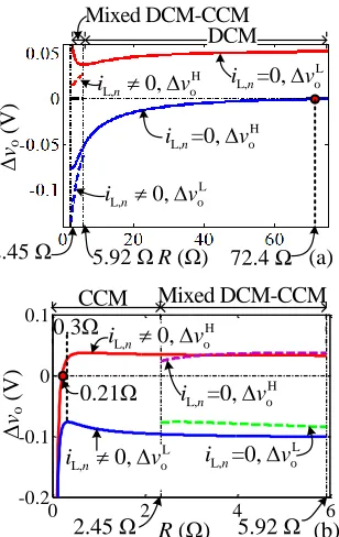
R (Ω) (a)
Δ
vo
(
V
)
DCM
72.4 Ω 5.92 Ω
Mixed DCM-CCM
2.45 Ω
H L,n=0, o
i v
L L,n 0, o
i v
L L,n=0, o
i v
H L,n 0, o
i v
0 2 4 6
-0.2 -0.1 0 0.1
R (Ω) (b)
Δ
vo
(
V
)
Mixed DCM-CCM CCM
H L,n=0, o
i v
L L,n=0, o
i v
2.45 Ω 5.92 Ω
0.21Ω
H L,n 0, o
i v
L L,n 0, o
i v
0.3Ω
[image:4.612.99.253.52.296.2]
Fig. 4. Output voltage variations of the PCC-PT controlled buck converter: (a) DCM and mixed DCM-CCM and (b) mixed DCM-CCM and CCM.
of a switching cycle. Thus when iL, n = 0, iC, n =−vo/R.
From (3) and (6), output voltage variation Δvo within one switching cycle is
o ( 1) C
2 2
in C, peak o C, in C, peak o C, o 2
o in o in o
1
7
( ) ( ) ( 2 )
2 ( ) ( ) 2
nT
n T
n n
v i dt
C
L v I v i L v I v i v L RT
Cv v v RC v v R C
where Δvo=voHfor PH and Δvo= L o
v
for PL.
With the same circuit parameters as given in section II, Fig.4(a) shows output voltage variations H
o
v
and L
o
v
of the PCC-PT controlled DCM buck converter, where solid lines show H
o
v
and L o
v
for Case 1 when the converter operates in DCM, that is, iC, n=−vo/R, and dotted lines showvoH and
L o
v
for Case 2 when the converter operates in mixed DCM-CCM, that is, iC, n ≠−vo/R.
For 2.45 Ω<R<5.92 Ω, the converter operates in mixed DCM-CCM, voH>0 and voL<0 are always satisfied as shown in Fig. 4(a). For R > 5.92 Ω, the converter operates in DCM,
H o
v
and voL increase with increased R, voH> 0 and voL< 0 until R increases to R = 72.4 Ω. For R > 72.4 Ω, voL> 0, that is, even if PL is selected as the active control pulse, the output voltage cannot decrease, and the PCC-PT controller cannot regulate the converter any more.
2) Output Voltage Variation of Case 4 (Case 3)
From (4) and (6), output voltage variation Δvo within one switching cycle is
2 2
in C, peak C, in C, peak o C, o
o 2
in o in o
( ) ( )
( ) 2
2 ( )
n n
Lv I i v I v i T v T
v
C v v LC
C v v
(8)
With the same circuit parameters as given in section II,
output voltage variationsvoHandvoLof the PCC-PT controlled buck converter operating in CCM and mixed DCM-CCM are shown in Fig. 4(b). In Fig. 4(b), solid lines show H
o
v
and L
o
v
for Case 4 when the converter operates in CCM, that is, iC,n≠−vo/R, and dotted lines showvoH and
L o
v
for Case 3 when the converter operates in mixed DCM-CCM, that is, iC, n
=−vo/R.
When 2.45 Ω<R<5.92 Ω, the converter operates in mixed DCM-CCM, voH>0 and voL<0 are always satisfied as shown in Fig. 4(b). When R < 2.45 Ω, the converter operates in CCM, with the decrease of R, voH decreases and voL increases slightly. When R<0.3 Ω, both voH and voL decrease dramatically. When R<0.21 Ω, H
o
v
<0, that is, even if PH is selected as the active control pulse, the output voltage cannot increase, and the PCC-PT controller cannot regulate the converter any more.
B. Circuit Parameter Design of the PCC-PT Controlled Buck Converter
From the previous discussion, for the PCC-PT controlled buck converter, when a high power control pulse PH is applied, the output voltage variation may be lower than zero, that is,
H o
v
> 0 is not satisfied, and when a low power control pulse PL is applied, the output voltage variation may be larger than zero, that is, L
o
v
< 0 is not satisfied. Thus, H o
v
> 0 and L o
v
< 0 should be considered in the parameter design. The design of control parameters follows.
For a light load condition, from (7), as iC, n = −vo/R, voL< 0 and H
o
v
> 0:
2
L in o o o
C, peak
in
2(v v v T) v I
RLv R
(9a)
2
H in o o o
C, peak
in
2(v v v T) v I
RLv R
(9b)
For a heavy load condition, from (8), as voL< 0 and voH> 0:
2 in o
C, peak C, C, peak
2 2
2 o in o o in o
C, C, 2
in in
( )
2( )
2 ( ) ( )
[ ] 0
n
n n
v v T
I i I
L
v v v T v v v T
i i
Lv L v
(10a)
which can be rewritten as
C, o
in o C, peak C,
in
2
( )
[1 1 n ]
n
Li v T
v v T
I i
L v T
(10b)
To ensure voH >0, IC, peak should be smaller than the minimum of the right part of (10b), which occurs when iC, n
=−vo/R
o in o o o
C, peak
in
( ) 2
[1 1 ]
v v v T Lv Rv T
I
R L Rv T
[image:4.612.315.565.528.650.2]Thus, (9) and (10c) should be satisfied for the parameter design of the PCC-PT controlled buck converter.
C. Output Power Range
Base on the previous discussion, under a light load condition, the PCC-PT controlled buck converter operates in DCM. With increased load power, converter goes into mixed DCM-CCM, and then goes into CCM. Thus, the minimum and maximum load powers Pmin and Pmax occur in DCM and CCM, respectively.
When the converter operates in DCM, the power from the input power source is completely transferred to the load within one switching cycle. Assuming the converter is lossless, then the power delivered from input power source to the load in one switching cycle is given by [9]
2 o in
DCM in ave C, peak
in o
( )
2( )
v Lv
P v I I
v v T R
(11)
where Iave is the average current flowing through S in a switching cycle. When PH is selected, PDCM =PDCMH ; and when
PL is selected, PDCM =PDCML , that is H
DCM o ref
DCM L
DCM o ref
, if , if
P v V
P
P v V
.
From (11), PDCM varies with the variation of load resistance
R, rather than fixed as with the conventional PT controlled buck converter [9]. For the PCC-PT controlled buck converter,
H DCM
P and L DCM
P should satisfy 2
H o
DCM o
2
L o
DCM o
,
. v
P P
R v
P P
R
(12)
where Po is load power.
When the converter operates in CCM, the inductor may store or release energy in one switching cycle, thus load power not only transferred from input power but also from the energy stored in the inductor. The input power Pin in one switching cycle is
2
in on o
in in ave (L, C, peak )
2 n
v t v
P v I i I
T R
(13)
From (2) and (4), iL, n+1 can be obtained as iL, n+1=IC, peak+vo/R −vo(T−ton)/L. The energy variation of the inductor ∆EL is
2 2
L ½ (L, n+1 L, n)
E L i i
(14) Then the power delivered from the input power source to the load in one switching cycle is
L CCM in
E
P P
T
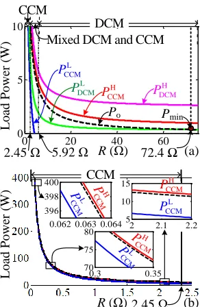
(15) With the same circuit parameters as given in section II,PDCMH , L
DCM
P , PCCMH , PCCML and Po with respect to R are shown in Fig. 5. As shown in Fig. 5(a), all decrease with increased R. For R > 5.92 Ω, the converter operates in DCM, as shown in Fig. 5(a). For R > 72.4 Ω, PDCML > Po, that is, when PL is selected as a control pulse, more power than load power Po is delivered from input power source to the load, which increases the output
0 20 40 60
0 5 10
R (Ω) (a)
L
o
ad
P
o
w
er
(
W
)
CCM
Mixed DCM and CCM DCM
Po Pmin L
CCM P
H CCM
P L DCM
P H
DCM
P
2.45 Ω 5.92 Ω 72.4 Ω
L
o
ad
P
o
w
er
(
W
)
R (Ω) (b) CCM
0.062 0.063 0.064 396
398 400
0.3 0.35
70 75
80 2 2.1 2.2
5 10 15
H CCM
P L CCM P
L CCM P
H CCM
P
L CCM P
H CCM
P
2.45 Ω
Fig. 5 The output powers of PCC-PT controlled buck converter: (a) the output power range of PCC-PT controlled buck converter and (b) zoom in view of (a).
voltage rather than decreasing it. Thus, as with conventional PT control, PL of the PCC-PT controller determines the minimum load power Pmin, which can be calculated from (12) as
2 o in o
min o C, peak
in
2
o in o in o
o o C, peak
in in
( )
( ) ( )
( 2 )
v v v T
P v I
Lv
v v v T v v T
v v I
Lv Lv
(16)
For 5.92 Ω < R < 72.4 Ω, as shown in Fig. 5(a), L DCM
P < Po < H
DCM
P , that is, in this condition, when PH is selected, more power than load power Po is delivered from the input power source to the load, which makes output voltage increase; and when PL is selected, less power than load power Po is delivered from the input power source to the load, which decreases the output voltage. Thus, PCC-PT control can adjust the buck converter output voltage by selecting PH or PL.
For 2.45 Ω < R < 5.92 Ω, the converter operates in mixed DCM-CCM, as shown in Fig. 5(a), both L
DCM
P <Po< PDCMH and L
CCM
P <Po<PCCMH are satisfied, that is, the PCC-PT controller can control the buck converter.
For R < 2.45 Ω, the converter operates in CCM, as shown in Fig. 5(b), it always has PCCML <Po<PCCMH , thus, the converter can be controlled at heavy load conditions. Different from conventional PT control, the maximum load power of the PCC-PT controlled buck converter does not only depend on PH, the output power can be high if the input power source can provide sufficient power.
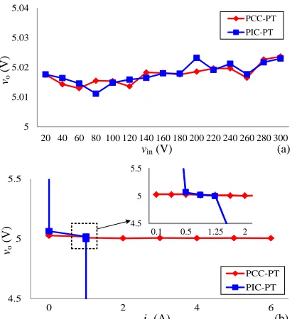
[image:5.612.368.514.51.275.2]vo
(
V
)
5 5.01 5.02 5.03 5.04
20 40 60 80 100 120 140 160 180 200 220 240 260 280 300 PCC-PT PIC-PT
vin (V) (a)
vo
(
V
)
4.5 5 5.5
0 2 4 6
PCC-PT PIC-PT
io (A) (b) 4.5
5 5.5
0.1 0.5 1.25 2
Fig. 6. Circuit performances: (a) line regulations of PCC-PT and PIC-PT controlled buck converters, and (b) load regulations of PCC-PT and PIC-PT controlled buck converters.
D. Line and Load Regulation
With the same circuit parameters as given in section II, line regulations of PCC-PT controlled buck converter and peak inductor current PT (PIC-PT) controlled buck converter are shown in Fig. 6 (a). The line regulations of PCC-PT and PIC-PT controlled buck converters for input voltage varying from 20 V to 300 V are 0.103% and 0.112%, respectively. PCC-PT and PIC-PT controlled buck converters have the similar line regulations.
Load regulations of PCC-PT and PIC-PT controlled buck converters with vin=20 V are shown in Fig. 6 (b), note that the x-axis in zoom-in window is at uneven increments. The load regulation of PCC-PT controlled buck converter from a minimum output current (0.1 A) to 6 A is 0.437%. The load regulation of PIC-PT controlled buck converter from a minimum output current (0.5 A) to a maximum output voltage current (1.25 A) is 1.305%. From Fig. 6 (b), PCC-PT controlled buck converter has wider load range and better load regulation than that of PIC-PT controlled buck converter.
IV. DISCRETE ITERATION MODEL
To verify the analysis in Section III, a discrete iteration model of the PCC-PT controlled buck converter, with output capacitor ESR considered, is established in this section. A. Operation States
For the PCC-PT controlled buck converter, when switch S is turned on and diode D is turned off, the converter operates in switch state 1. During this switch state, the inductor current iL and capacitor voltage vC are
ESR L
in L C
ESR ESR
C
L C
ESR ESR
( )
( ) ( ),
( ) 1
( ) ( ).
RR
di t R
L v i t v t
dt R R R R
dv t R
C i t v t
dt R R R R
(17)
which can be solved as
C C, in 1 in
in in
L L, 2
( )= [( ) cos( ) sin( )] ,
( ) [( ) cos( ) sin( )] . t
n
t n
v t e v v t k t v
v v
i t e i t k t
R R
(18)
where α, k1 and k2 are ESR
ESR
2( )
RR C L
R R LC
,
2
ESR
( )
R
R R LC
,
ESR
1 L, C, in
ESR ESR
+
( ) n 2( ) n
RR C L
R
k i v v
R R C R R LC
,
ESR
2 L, C, in
ESR ESR
( )
2( ) n ( ) n
L RR C R R L
k i v v
R R LC R R L RL
.
As iC(ton) = IC, peak, from (18), the time duration ton of switch state 1 is
2
2 2 1 3
on
1 2
t
(19) where
2
1 L, C, 2 1
ESR
2( )( ) ( )
( ) n n
R
Ri v Rk k
R R LC
,
2 (Rk2 k1) (RiL,n vC,n)
, and
3 (RiL,n vC,n) (R RESR)IC, peak
.
After time duration ton, switch S is turned off and diode D is turned on, the converter operates in switch state 2. During this switch state, the inductor current iL and capacitor voltage vC are
ESR L
C L
ESR ESR
C
L C
ESR ESR
( )
( ) ( ),
( ) 1
( ) ( ).
RR
di t R
L v t i t
dt R R R R
dv t R
C i t v t
dt R R R R
(20)
which can be solved as
C C on 3
L L on 4
( )= [ ( ) cos( ) sin( )], ( ) [ ( ) cos( ) sin( )].
t
t
v t e v t t k t
i t e i t t k t
(21)
where iL(ton) = IL, peak and vC(ton) are the initial conditions of switch state 2, vC(ton) can be obtained from (18), and k3 and k4 in (21) are
ESR
3 L on C on
ESR ESR
( ) ( )
( ) 2( )
RR C L
R
k i t v t
R R C R R LC
,
ESR
4 L on C on
ESR ESR
( ) ( )
2( ) ( )
RR C L R
k i t v t
R R LC R R L
.
In switch state 2, iL decreases. When iL decreases to zero before the end of the switching cycle, the converter operates in DCM, otherwise, it operates in CCM.
When the PCC-PT controlled buck converter operates in CCM, time duration toff in this switch state is
off on
t T t (22) When converter operates in DCM, as iL(t2) = 0, where t2 =
ton+toff from (21), the time duration toff in this switch state is C, peak C on
off
3 4
( ) 1
arctanRI v t
t
k Rk
(23)
After iL decreases to zero, it remains at zero, and both switch
[image:6.612.72.281.49.274.2]capacitor voltage vC are L
C
C ESR ( )
0,
( ) 1
( ). di t
L dt dv t
C v t
dt R R
(24)
which can be solved as ESR
C C 2
L
( )
( )= ( ) ,
( ) 0.
t
R R C
v t e v t
i t
(25)
where vC(t2) is the initial condition of switch state 3, which can be obtained from (21). The time duration of switch state 3 is toff2 = T−ton−toff.
B. Discrete Iteration Model
From (18), (19), (21) and (22), the discrete iteration model of the PCC-PT controlled CCM buck converter can be derived as
off
off
C, 1 C, in 1
in off off
in
L, 1 L, 2
in
off off
[( ) cos sin ]
[cos( ) sin( )] ,
[( ) cos sin ]
[cos( ) sin( )] .
T
n n
t
T
n n
t
v e v v T k T
v t t e
v
i e i T k T
R
v L R
t t e
R L
(26)
From (18), (19), (21), (23) and (25), the discrete iteration model of the PCC-PT controlled DCM buck converter is
off1 on off
ESR
off1 off ESR
( )
( )
C, 1 C, in on off
1 on off
( )
in off off
L, 1
[( ) cos ( )
sin ( )]
[cos( ) sin( )] ,
0.
t t t
R R C
n n
t t R R C
n
v e v v t t
k t t
v t t e
i
(27)
C. Effects of Circuit Parameters on the Stability of the PCC-PT Controlled Buck Converter
Based on discrete iteration models (26) and (27), the effect of load resistance on the steady-state performance of the PCC-PT controlled buck converter is studied in this section.
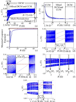
Fig. 7(a) shows the bifurcation diagrams of the output voltage vo with load resistance R as the bifurcation parameter. As shown in Fig. 7(a), with increased R, the converter goes from multi-periodicities to period-1 at R =72.4 Ω, which is consistent with the analysis in Section III.
Fig. 7(b) shows the bifurcation diagrams of inductor current iL with load resistance R as the bifurcation parameter. Fig. 7(b) shows the operating modes of the PCC-PT controlled buck converter: for R < 2.36 Ω, inductor current orbits are always higher than zero, that is, the converter operates in CCM; for 2.36 Ω < R < 5.69 Ω, there exists iL =0, that is, the converter operates in mixed DCM-CCM; and for R > 5.69 Ω, all inductor current orbits decrease to zero and remain at zero, that is, the converter operates in DCM. The small difference between the ranges of these three operating modes and the ranges calculated in Section III is caused by the ESR and the accuracy of model. Fig. 7(c) shows that for all R, the maximal Lyapunov exponent is less than zero, which illustrates that the converter is stable.
Fig. 7(d)-(g) are the zoom-in views of Fig. 7 (a), where some
R (Ω) (d)
0 20 40 60
-0.3 -0.2 -0.1 0
R (Ω) (c)
M
ax
im
al
L
y
ap
u
n
o
v
E
x
p
o
n
en
t
vo
(
V
)
2PH-1PL
14.93 Ω 15.08 Ω
R (Ω) (e)
vo
(
V
)
1PH-1PL
R (Ω) (f)
vo
(
V
)
2PH-1PL
5PH-2PL 5PH-3PL
8.62 Ω 8.81 Ω
R (Ω) (g)
vo
(
V
)
3PH-1PL
[image:7.612.76.566.41.422.2]1.12 Ω 1.61 Ω
Fig. 7. Effects of circuit parameters on the steady-state performance of PCC- PT controlled buck converter: (a) bifurcation diagram of vo with the increase of
R, (b) bifurcation diagram of iL with the increase of R, (c) maximal Lyapunov
exponent with the increase of R, (d) zoom in view of (a), (e) zoom in view of (a), (f) zoom in view of (a), and (g) zoom in view of (a).
special periodicities are presented. Fig. 7 (d) and (e) show bifurcation diagrams when the converter operates in DCM. The converter operates in period-3 with control pulse combination 1PH-2PL for 14.93 Ω < R < 15.08 Ω, and operates in period-2 with control pulse combination 1PH-1PL for 8.62 Ω < R < 8.81 Ω. Fig. 7 (f) shows bifurcation diagrams when the converter operates in mixed DCM-CCM. Wth the decrease of R, the converter operates in period-8 with control pulse combination 5PH-3PL, period-3 with control pulse combination 2PH-1PL, and period-7 with control pulse combination 5PH-2PL. The same control pulse combination, such as period-3 with control pulse combination 2PH-1PL, can exist in different operating modes of the PCC-PT controlled buck converter. Fig. 7 (g) shows bifurcation diagrams when the converter operates in CCM. The converter operates in period-4 with control pulse combination 3PH-1PL for 1.12 Ω<R<1.61 Ω. From Fig. 7(d)-(g), with increased R, the ratio between the number of high power control pulse μH and low power control pulse μL increases.
V. SIMULATION AND EXPERIMENTAL RESULTS
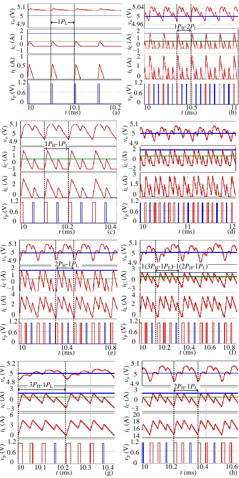
[image:7.612.313.566.52.390.2] [image:7.612.47.215.53.172.2] [image:7.612.45.300.229.456.2]current iL and switch driving voltage vp for R = 75 Ω. The load is too light to be controlled by the PCC-PT controller, vo is always higher than reference voltage Vref, low power control pulse PL is thus continuously applied as the control pulse, and the converter operates in period-1 with the control pulse repetition cycle consisting of only PL.
Fig. 8(b) and (c) show the waveforms for R = 15 Ω and R = 8.7 Ω. The converter operates in DCM. For R = 15 Ω, the converter operates in period-3 with control pulse combination 1PH-2PL. For R = 8.7 Ω, converter operates in period-2 with control pulse combination 1PH-1PL.
Fig. 8(d)-(f) show the waveforms for R = 5.1 Ω, R = 4 Ω and R=2.9 Ω. The converter operates in mixed DCM-CCM. For R=5.1 Ω, the converter operates in period-8 consisting of 5PH and 3PL, and the control pulse combination is 2(2PH-1PL) -1(1PH-1PL). For R=4 Ω, the converter operates in period-3 with control pulse combination 2PH-1PL. For R=2.9 Ω, the converter operates in period-7 which consists of 5H and 2PL, and the control pulse combination is 1(3PH-1PL)-1(2PH-1PL).
Fig. 8(g)-(h) show the waveforms for R = 1.5 Ω and R = 0.3 Ω. The converter operates in CCM. For R = 1.5 Ω,the converter operates in period-4 with control pulse combination 3PH-1PL. For R = 0.3 Ω, the converter operates in period-3 with control pulse combination 2PH-1PL. Simulation results of Fig. 8 are consistent with the theoretical analysis results.
Fig. 9 shows transient response of PCC-PT controlled buck converter under step load current variation from 5 A to 1 A and from 1 A to 5 A, respectively. As shown in Fig. 9(a), when load current io step decreases at time t=10.5 ms, as inductor current
iL can not change immediately, and because of iC=iL−io, output capacitor current iC abruptly jumps to 3.548 A which is larger than H
C, peak
I , the switch S is then turned off immediately. Three low power control pulses are selected as active control pulses to decrease the output voltage. After four switching cycles, the converter goes into a steady-state. The transient time is 4 switching cycles (200 μs) and the output voltage overshoot is 0.213 V (4.26%).
When load current io step increases at time t=10.5 ms as shown in Fig. 9(b), iC decreases to −4.695A. Two high power control pulses are selected as active control pulses to increase the output voltage. After 2 switching cycles, the converter goes into a steady-state. The transient time is 2 switching cycles (100 μs) and the output voltage sag is 0.135 V (2.7%).
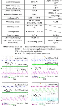
By using the same circuit parameters, experimental results of the PCC-PT controlled buck converters are shown in Fig. 10. For R = 15 Ω, the converter operates in period-3 with control pulse combination 1PH-2PL, as shown in Fig. 10(a). For R = 8.7 Ω, the converter operates in period-2 with control pulse combination 1PH-1PL, as shown in Fig. 10(b). As shown in Figs. 10(a) and (b), the converter operates in DCM.
Fig.10(c) shows that for R = 4 Ω, the converter operates in mixed DCM-CCM and in period-3 with control pulse combination 2PH-1PL. Fig.10(d) shows that for R = 0.3 Ω, the converter operates in CCM and in period-3 with control pulse combination 2PH-1PL. These experimental results verify the theoretical analysis and simulation results.
10 10.1 10.2
t (ms) (b) 5.04 5 4.96 2 1 0 vo ( V ) iL ( A ) 2 1 0 iC ( A ) −1 1.2 0.6 0 vp ( V )
10 10.5 11
1PH-2PL
t (ms) (a) 5.1 5 4.9 1 0.5 0 vo ( V ) iL ( A ) 2 1 0 iC ( A ) −1 1.2 0.6 0 vp ( V ) 1PL
10 11 12 10 10.2 10.4
t (ms) (c) 5.1 5 4.9 4 2 0 vo ( V ) iL ( A ) 2 1 0 iC ( A ) −1 1.2 0.6 0 vp ( V )
1PH-1PL
t (ms) (d) 5.1 5 3 1.5 0 vo ( V ) iL ( A ) 2 0 iC ( A ) −2 1.2 0.6 0 vp ( V ) 4.9
10 10.2 10.4 10.6 10.8 t (ms) (f) 5.1 5 4.9 4 2 0 vo ( V ) iL ( A ) 3 0 iC ( A ) −3 1.2 0.6 0 vp ( V )
1(3PH-1PL)-1(2PH-1PL)
10 10.4 10.8 t (ms) (e) 5.1 5 4.9 4 2 0 vo ( V ) iL ( A ) 2 1 0 iC ( A ) −1 1.2 0.6 0 vp ( V )
2PH-1PL
10 10.2 10.4 10.6 10 10.1 10.2 10.3 10.4
t (ms) (g) 5 4.8 6 0 vo ( V ) iL ( A ) 3 0 iC ( A ) −3 1.2 0.6 0 vp ( V )
3PH-1PL
t (ms) (h)
vo ( V ) iL ( A ) iC ( A ) vp ( V )
2PH-1PL
[image:8.612.320.561.49.531.2]3 5.1 5 4.9 3 0 −3 20 18 14 1.2 0.6 0 5.2 16
Fig. 8. Simulation result: (a) DCM, R = 75 Ω, (b) DCM, R = 15 Ω, (c) DCM, R
= 8.7 Ω, (d) mixed DCM-CCM, R = 5.1 Ω, (e) mixed DCM-CCM, R = 4 Ω, (f) mixed DCM-CCM, R = 2.9 Ω, (g) CCM, R = 1.5 Ω, and (h) CCM, R = 0.3 Ω.
10 10.5 11 t (ms) (a)
10 10.5 11 5.2 5 4.8 3 0 −3 vo ( V ) iC ( A ) 6 3 io ( A ) 0
t (ms) (b) 5.4 1.2 0.6 vp ( V ) 0 5.2 5 4.8 2.5 0 −5 vo ( V ) iC ( A ) 6 3 io ( A ) 0 5.4 1.2 0.6 vp ( V ) 0
1PH-3PL
2PH 3.548 A 5.213 V −4.695 A −2.5 4.865 V
[image:8.612.317.564.564.688.2](b)
vo(500mV/div)
io(500 mA/div)
iL(2 A/div)
(a)
vo(500mV/div)
io(500 mA/div)
iL(2 A/div) 1PH-2PL
1PH-1PL
(d)
vo(500mV/div)
iL(5 A/div)
vp(5 V/div) (c)
vo(500mV/div)
io(500 mA/div)
iL(2 A/div) 2PH-1PL
[image:9.612.45.299.85.513.2]2PH-1PL
Fig. 10. Experimental results: (a) DCM, R = 15 Ω, (b) DCM, R = 8.7 Ω, (c) mixed DCM-CCM, R = 4 Ω, and (d) CCM, R = 0.3 Ω.
(b)
vo(1 V/div)
io(5 A/div)
iC(2 A/div)
1PH-1PL vo(5 V/div)
(a)
vo(1 V/div)
io(5 A/div)
iC(2 A/div) 1PH-4PL
vo(5 V/div) 3.2 A
5.2V
4.8 V
−2.8 A
Fig. 11. Transient response experimental results of PT and PCC-PT controlled buck converter: (a) load current step decreases from 5A to 1 A, and (b) load current step increases from 1 A to 5 A.
Fig. 11 shows the transient response experimental results of conventional PT and PCC-PT controlled buck converter under step load variation from 5 A to 1 A and from 1 A to 5 A, respectively. As shown in Fig. 11(a), when load current io step
decreases from 5 A to 1 A, output capacitor current iC increases to 3.2 A, which is larger than H
C, peak
I , the switch S is then turned off immediately. Four low power control pulses are selected as active control pulses to decrease the output voltage. After five switching cycles, the converter goes into a steady-state. The transient response time is 5 switching cycles and the output voltage overshoot is about 0.2 V (4%). As shown in Fig. 11(b), when load current io step increases from 1 A to 5 A, iC decreases to −2.8 A. One low power control pulse and one high power control pulse are selected as active control pulses to increase the output voltage. After 2 switching cycles, the converter goes into a steady-state. The transient response time is 2 switching cycles and the output voltage sag is 0.2 V (4%), approximately. Moreover, the comparisons with the previous ripple-based control techniques are shown in Table I. From Table I, because of different switching frequencesf, the comparative study of transient responses of different control techniques is not obvious by comparing recovery times TR. Thus, the switching cycle numbers of transient process, which reduces the effect of switching frequence, are considered to evaluate the transient performance. For PCC-PT controlled buck converter, only 2-5 switching cycles are required to get into steady state, which is less than the other control techniques. Moreover, the transient response of PCC-PT controlled converters can be improved by increasing switching frequency.
VI. CONCLUSION
In this paper, based on a discrete control technique, conventional PT control, for switching dc-dc converters, a PCC-PT control technique for the buck converter is proposed and analysed. Different from PT control, PCC-PT control uses peak capacitor current as a feedback control variable to generate high power control pulse PH and low power control pulse PL. The output voltage variations, voH and
L o
v
, of the
TABLE I. COMPARISON TABLE WITH THE PREVIOUS WORKS
Proposed in this paper Ref.[4] Ref. [14,15] Ref. [16] Ref. [17] Ref. [18]
Control technique PCC-PT Digital enhanced V
2-type
COT PIC-PT PCM-BF IPR VCM-PT
Input voltage (vin) 20 V 12 V 20 V 20 V 15 V 12 V
Output voltage (vo) 5 V 1.2 V 5 V 6 V 5 V 5 V
Output capacitor (C) 440 μF 1600 μF 440 μF 1880 μF 800 μF 470 μF
Switching frequency (f) 20 kHz 15 MHz (Maximum
frequency) 20 kHz 16.7-66.7 kHz 20 kHz 40-125 kHz
Load range (Po) 0.35-119.05 W 2.5-6.25 W 6-12 W 0.5-4.9 W 6-13 W
Operating modes DCM, Mixed
DCM-CCM, CCM CCM DCM DCM DCM CCM
Line regulation 0.103 % (20 V-300 V)
0.112 % (20 V-300 V)
Load regulation 0.437 % (0.1 A-6 A) 1.305 %
(0.5 A-1.25 A)
1.386% (0.08-0.8 A)
Load transient 1 -5 A 6 -18 A 1 -2 A 1-2 A 0.08-0.8 A
Recovery time (TR) 50-250 μs 38 μs 1.8 ms 125 μs 50 μs
Switching cycle number
for recovery 2-5 Switching cycles
About 50 Switching cycles
9 Switching cycles
2-8 Switching cycles
1 Switching cycles
Abbreviations: PCM-BF — Peak current mode bifrequency control; ICRIF — Inductor current ripple injection feedback circuit; IPR — Improved pulse regulation;
[image:9.612.47.297.545.652.2]PCC-PT controlled buck converter with output load variation are studied; from which, control parameter design is presented. From theory and simulation analysis, within a wide load range,
H o
v
> 0 and L o
v
< 0 can always be satisfied, that is, the fast-scale oscillation in a conventional PT controlled buck converter can be eliminated. In order to better understand the characteristics of the PCC-PT control buck converter, an accurate discrete iteration model of the PCC-PT controlled buck converter was established. From this model, the effects of circuit parameters on stability performance of the PCC-PT controlled buck converter operating in DCM, mixed DCM-CCM, and CCM are studied. The presented simulation and experimental results verify the analysis.
REFERENCES
[1] C. Ji-Soo, O. Hyoung-Seok, J. Young-Hyun, and K. Bai-Sun, "Fast Output Voltage-Regulated PWM Buck Converter With an Adaptive Ramp Amplitude Control," IEEE Trans. Circuits Syst. II: Express Briefs, vol. 60, pp. 712-716, Oct. 2013.
[2] Y. Bing, L. Xin-Quan, W. Hong-Yi, and S. Ling-Feng, "High-Efficient Hybrid Buck Converter With Switch-on-Demand Modulation and Switch Size Control for Wide-Load Low-Ripple Applications," IEEE Trans.
Microw. Theory Tech., vol. 61, pp. 3329-3338, Sep. 2013.
[3] S. Maity and Y. Suraj, "A fixed frequency dual-mode DC-DC buck converter with fast-transient response and high efficiency over a wide load range," in 2013 Twenty-Eighth Annual IEEE Applied Power Electronics
Conference and Exposition (APEC), 2013, pp. 415-420.
[4] K. Cheng, F. Yu, F. C. Lee, and P. Mattavelli, "Digital Enhanced V2-Type Constant On-Time Control Using Inductor Current Ramp Estimation for a Buck Converter With Low-ESR Capacitors," IEEE Trans.Power Electron.,
vol. 28, pp. 1241-1252, March 2013.
[5] G. Zhou, J. Xu, and J. Wang, "Constant-Frequency Peak-Ripple-Based Control of Buck Converter in CCM: Review, Unification, and Duality,"
IEEE Trans. Ind. Electron., vol. 61, pp. 1280-1291, March 2014.
[6] T. Qian, W. Wu, and W. Zhu, "Effect of Combined Output Capacitors for Stability of Buck Converters With Constant On-Time Control," IEEE
Trans. Ind. Electron., vol. 60, pp. 5585-5592, Dec. 2013.
[7] T. Qian, "Study of Subharmonic Oscillation Mechanism and Effect of Circuit Propagation Delay for Buck Converters With Constant On-Time Control," IEEE Trans. Circuits Syst. I: Regular Papers, vol. 60, pp. 788-795, March 2013.
[8] M. Ferdowsi, A. Emadi, M. Telefus, and C. Davis, "Pulse regulation control technique for flyback converter," IEEE Trans.Power Electron., vol. 20, pp. 798-805, Aug. 2005.
[9] S. Jin, X. Jianping, B. Bocheng, and Y. Tiesheng, "Effects of Circuit Parameters on Dynamics of Current-Mode-Pulse-Train-Controlled Buck Converter," IEEE Trans. Ind. Electron., vol. 61, pp. 1562-1573, March 2014.
[10] J. Wang, B. Bao, J. Xu, G. Zhou, and W. Hu, "Dynamical Effects of Equivalent Series Resistance of Output Capacitor in Constant On-Time Controlled Buck Converter," IEEE Trans. Ind. Electron., vol. 60, pp. 1759-1768, May 2013.
[11] J. Sun, "Characterization and performance comparison of ripple-based control for voltage regulator modules," IEEE Trans.Power Electron., vol. 21, pp. 346-353, March 2006.
[12] R. Redl and S. Jian, "Ripple-Based Control of Switching Regulators--An Overview," IEEE Trans.Power Electron., vol. 24, pp. 2669-2680, Dec. 2009.
[13] J. Wang, J. Xu, G. Zhou, and B. Bao, "Pulse-Train-Controlled CCM Buck Converter With Small ESR Output-Capacitor," IEEE Trans. Ind. Electron.,
vol. 60, pp. 5875-5881, Dec. 2013.
[14] J. Sha, J. Xu, L. Xu, and S. Zhong, "Capacitor current feedback pulse train control technique for switching DC-DC converters," Electron. Lett., vol. 50, pp. 1088-1090, July 2014.
[15] J. Sha, J. Xu, S. Zhong, S. Liu, and L. Xu, "Control Pulse Combination-Based Analysis of Pulse Train Controlled DCM Switching DC-DC Converters," IEEE Trans. Ind. Electron., vol. 62, pp. 246-255, Jan. 2015.
[16] J. Wang, and J. Xu, "Peak Current Mode Bifrequency Control Technique for Switching DC–DC Converters in DCM With Fast Transient Response and Low EMI," IEEE Trans.Power Electron., vol. 27, pp. 1876-1884, Apr. 2012.
[17] M. Qin, and J. Xu, "Multiduty Ratio Modulation Technique for Switching DC–DC Converters Operating in Discontinuous Conduction Mode, " IEEE
Trans. Ind. Electron., vol. 60, pp. 1819 - 1830, Oct. 2013.
[18] J. Sha, J. Xu, S. Zhong, and S. Liu, "Valley current mode pulse train control technique for switching DC-DC converters," Electron. Lett., vol. 50, pp. 311 - 313, Feb. 2014.
Jin Sha was born in Shandong, China, in 1987. She received the B.S. degree in electrical engineering and automation from Southwest Jiaotong University, Chengdu, China, in 2009, where, she is currently pursuing the Ph.D. degree in the School of Electrical Engineering. During her Ph. D studies, she was a sponsored visiting researcher in the Department of Electronic and Electrical Engineering, University of Strathclyde, Glasgow, UK, from Sep. 2013 to Aug. 2015.
Her research interests include control technique of switching-mode power supplies and modeling, simulation and analysis of dynamical behavior of switching dc–dc converters.
Duo Xu was born in Sichuan, China, in 1992. He received the B.S. degree in electronic information engineering from University of Science and Technology of China, Hefei, China, in 2014. He is currently pursuing the M.S. degree in the School of Electrical Engineering, Southwest Jiaotong University, Chengdu, China.
His research interests include control technique of switching-mode power supplies and modeling, simulation and analysis of topology of switching dc–dc converters.
Yiming Chen was born in Sichuan, China, in 1990. He received the B.S. degree in electrical engineering and automation from Southwest Jiaotong University, Chengdu, China, in 2013, where he is currently pursuing the Ph.D. degree in the School of Electrical Engineering.
His research interests include the ripple control technique of switching-mode power supply and the modeling of switching DC-DC converter.
Jianping Xu received the B.S. and Ph.D. degrees in electronic engineering from the University of Electronics Science and Technology of China, Chengdu, Sichuan, China, in 1984 and 1989, respectively.