Use of Confocal and Multiphoton Microscopy for the
evaluation of micro-optical components and emitters
J M Girkin1, E Gu1, C Griffin1, H. W. Choi1, M D Dawson1, G McConnell2
1
Institute of Photonics, Wolfson Centre, University of Strathclyde, 106 Rottenrow, Glasgow, G4 0NW, UK
2
Centre for Biophotonics, University of Strathclyde, 27 Taylor Street, Glasgow G4 0NR, UK
Running Title LED-lens microscopy
Contact; J M Girkin, email [email protected]
Tel 0141 553 4120 Fax 0141 552 1575 Institute of Photonics University of Strathclyde Glasgow
G4 0NW UK
Abstract
Introduction
Since the introduction of high resolution reliable commercial confocal microscopes in the mid 1980’s they have become one of the key tools for life science researchers, enabling routine three dimensional visualisation of structures with sub micron resolution(Pawley 1995). With the introduction of multiphoton excitation in the early 1990s by Denk et al. (1990) the ability to probe the sample at depth, with minimal damage, has become an increasingly important methodology. The rapid adoption of such techniques has lead optical physicists to develop and improve both laser sources and optical components to enable the techniques to become more widely adopted in the life sciences (Girkin 2003), but their use within physics has been limited. However, with the rapid expansion of interest and fabrication of micron sized optical components this situation is likely to change.
Semiconductor and device engineers routinely use electron microscopy to probe the structure of their devices and atomic force microscopy provides a powerful tool for the examination of surface structures, however, neither method provides information on the optical properties of the devices and they are not well suited to routine use on a
production line. In addition these techniques are not suitable for direct evaluation of a sample’s optical performance. Confocal microscopy has been previously applied to the examination of surface structures (O’Donnell 1999) but this work was undertaken on wafers rather than intact devices. There has also been a rapid expansion in the production of micro-optical emitters and components with dimensions of tens of microns which presents new challenges for evaluation compared to the more conventional devices with sizes of 100 microns upwards. Recently arrays of micro LEDs operating from 375 to 510nm, for example, have been produced by several groups (Jeon et al 2003, Ozden et al 2001, Jiang et al 2001) with anticipated applications ranging from displays to medical diagnostics. In addition matching optical components have also been produced (Choi et al 2004a) whose performance cannot be measured by conventional techniques.
We report here on the use of commercially available multiphoton and confocal
microscopes to evaluate the operation of such emitting and beam shaping devices. The techniques outlined are suitable for the examination of such devices in a production environment and may be suitable for on line monitoring of integrated optical devices in the longer term.
Method and Materials
Coherent Mira laser was used pumped with a 5W Verdi laser. Previously published work using this system(Girkin et al 2000) has shown lateral and axial resolutions close to the theoretical limit.
The LED devices used for the work have been previously described by Jeon (2003) and had emitting wavelengths from 370 to 510nm. All devices used were packaged in semiconductor carriers and driven using a conventional low current power supply. In order to image the micro lens arrays, the fabrication of which is described by Gu (2004), the samples were placed on a cover slip with the flat face in contact with the cover slip. This provided a stable base and made it easy to align the lens arrays under the
microscope. One sample was evaluated without the cover slip allowing direct access of the illumination light to the rear surface of the array with identical results to the cover slip method which was therefore used for simplicity.
Emission Characterisation
This was undertaken with the packaged LED devices mounted in a specially made holder enabling easy multi-axis alignment. The scan head was set into its scanning mode and using the 488nm line and a wide field lens (x10, 0.25NA) the reflection confocal image from the device was observed utilising a high contrast look-up table. The device was then adjusted angularly until the image showed even illumination across the device. This was required to ensure that the device was normal to the viewing axis. The illumination laser was then blocked and the required element(s) of the device switched on and XYZ images were then recorded from within the sample through to a height typically 50-100 microns above the surface. In one method the red krypton line was used to measure the surface profile of the device which was detected using an optical bandpass filter (647nm +/- 10nm) and photomultiplier arrangement, whilst the LED emission was recorded in the blue or green channels through the use of the standard dielectric filters (blue bandpass 470nm +/- 30nm, green 525nm +/- 25nm). This enabled the exact surface profile to be matched with the emission distribution. Care was taken to ensure that the images did not approach the saturation of the system and typically images were in the dynamic range region of 210 to 30 counts as the system was known to be linear with intensity in this region. Images were then analysed off line using Meta Morph V4.6 (Universal Imaging Inc) and Origin V7 (Origin Inc). Both manual and automated methods were used to examine the intensity maps and calculate the emission profiles.
Multiphoton Excitation
pixel dwell times of 10µs. XYZ images were then recorded scanning through the emission structure. The device was then switched on and electrically excited images taken matching the optically excited sections.
Lens Measurements
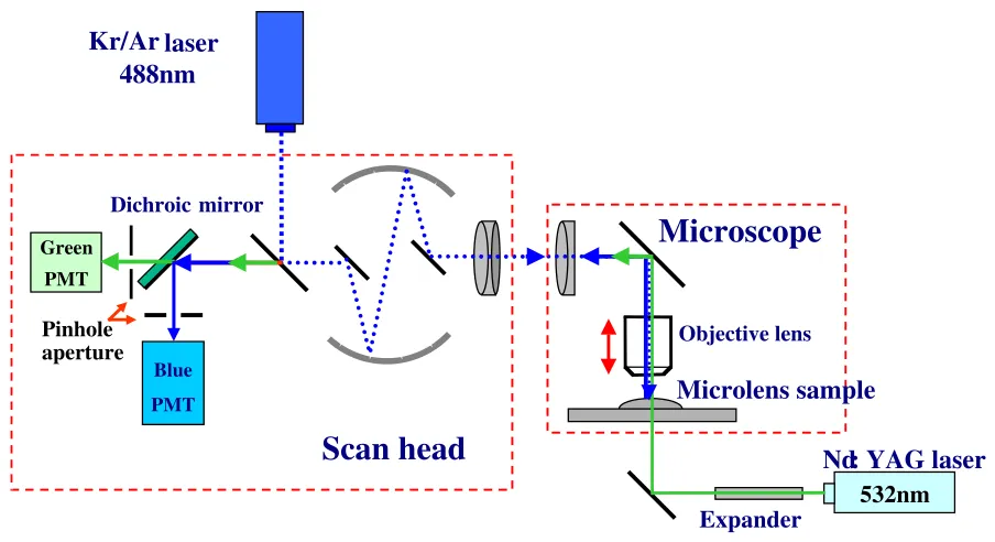
The optical arrangement used for the lens evaluation is shown in figure 1. Light from a lower power frequency doubled laser (Power Technology Inc.) was expanded using a x16 beam expander and directed up through the microscope stage using a conventional
aluminium coated plane mirror. Initially the conventional 488nm illumination laser beam was “parked” in the centre of the image and without the microscope objective this beam was overlapped with the through illumination beam. Full alignment of the through beam along the optical axis was checked using the confocal imaging system, ensuring even illumination over around 3mm of vertical travel of the lens. The micro lens array was then placed on the microscope stage either on a cover slip or in a special holder. The through light was detected in the green channel using a narrow band dielectric filter and the reflected 488nm light collected in the blue channel. It was thus possible to view the transmission through the lens and the surface profile simultaneously. The confocal pin-hole was adjusted for optimal axial sectioning (1.5 Airy disks) and an image taken around 30microns from the lens surface. XZ scans were then recorded using a line drawn through the centre of the original image. Tests were undertaken using complete XYZ stacks but were found to produce identical results to those using a single XZ line scan, with the latter method being quicker and requiring considerably less data storage space. The focal length of the lens was then calculated by analysis of the XZ section using a histogram plot of the intensity through the centre of the section.
Results
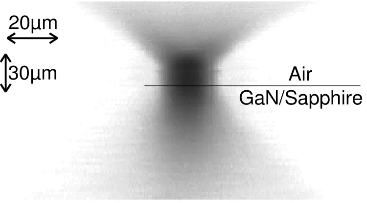
Figure 2 demonstrates a section through the reconstructed three dimensional data stack of the LED emission. Using the analysis method outlined above the cone angles for a number of devices was calculated and shown in table 1. In order to ensure that the results were not objective lens limited, for one sample an oil immersion objective lens (NA=1.4, times 20 magnification) was used and the resulting cone angle found to be identical to that measured using the 0.75 lens. The beam divergence results also fitted with the theoretical calculations. It should be noted that during the image analysis care had to be taken when measurements were made of the beam divergence within the substrate due to the high refractive index (n=1.8) of the substrate with the effective optical movement being therefore 1.8 times the physical movement of the lens. The images are corrected for this and the vertical scale is identical both above and below the surface, and equivalent to the optical path length in air.
demonstrating a lower electrically driven emission power compared to the multiphoton excited emission. In addition emission can be affected by the local micro-structure of each emitter. More recent devices show significantly more even illumination and a detailed examination of the full data available from this technique is currently underway and subject to a separate paper.
Typical XZ sections for the diamond lens measurements are shown in figure 4. The horizontal line shows the surface reflection image of the lens array with the effects of the lens on the collimated through illumination beam coming from this surface. The effective focal length of the lenses measured ranged from 5 to 500 microns and was in excellent agreement with the calculated values based upon AFM data of the profile of the lenses and are given in full by Gu et al (2004).
Discussion
References
Choi H W, Liu C, Gu E, McConnell G, Girkin J M, Watson I M, Dawson M D. 2004a. GaN micro-light-emitting diode arrays with monolithically integrated sapphire
microlenses. Appl. Phys. Lett. 84: 2253-2255
Denk W, Strickler J H, Webb W W. 1990. Two-photon excitation in laser scanning microscopy. Science 248: 73-76
Girkin J M. 2003. Optical physics enables advances in multiphoton imaging. J. Phys. D. 36: R250-R258
Girkin J M, Ferguson A I, Wokosin D L, Gurney A M. 2000. Confocal Microscopy using an InGaN violet laser diode at 406nm. Opt. Exp. 7 336-341
Gu E, Choi H W, Liu C, Griffin C, Girkin J M, Watson I M, Dawson M D, McConnell G, Gurney A M. 2004 Reflection/transmission confocal microscopy characterization of single crystal diamond microlens arrays. Appl. Phys. Lett. 84: 2754-2756
Jeon C W, Choi H W, Dawson M D. 2003. A novel fabrication method for a 64x64 matrix-addressable GaN-based micro-LED array. phys. Stat. Sol. (a) 200: 79-82
Jiang H X, Jin S X, Li J, Shakya J, Lin J Y. 2001. III- nitride microdisplays. Appl. Phys. Lett. 78: 1303-1305
O'Donnell K P, Tobin M J, Bayliss S C, Van der Stricht W. 1999. Confocal microscopy and spectroscopy of InGaN epilayers on sapphire. J. of microscopy 193: 105-108
Ozden I, Diagne M, Nurmikko A V, Han J, Takeuchi T. 2001. A Matrix Addressable 1024 Element Blue Light Emitting InGaN QW Diode Array. Phys. Stat. Sol. 188: 139-142
Table 1 Emission angle for four wavelengths of micro-LED arrays with a source diameter of 20µm.
Colour Wavelength (nm) Objective NA Beam divergence
(half angle)
Green 510 0.75 38.3°
Blue 468 1.35 38.3°
Blue 468 0.75 39.8°
UV 370 0.75 32.3°
Figure Legends
Figure 1 Optical configuration used for the evaluation of micro-lens arrays utilising both reflection and transmission confocal microscopy.
Figure 2 XZ Section of the emission profile of a 20µm diameter GaN micro-LED emitting at 460nm.
Figure 3a Two-photon excited emission from a GaN micro-LED array Figure 3b Emission from the same element as 3b using electrical excitation
Figure 1
Kr/Ar laser 488nm
532nm
Nd: YAG laser
Objective lens Dichroic mirror
PMT Microlens sample
Microscope
Pinhole aperture
PMT Green
Blue
Scan head
Figure 2