Thesis by Brian Standley
In Partial Fulfillment of the Requirements for the Degree of
Doctor of Philosophy
California Institute of Technology Pasadena, California
2012
c
⃝2012
Brian Standley
Except where otherwise noted, this work is licensed under the Creative Commons Attribution-ShareAlike 3.0 Unported License. To view a copy of this license, visit http://creativecommons.org/licenses/by-sa/3.0/or send a
Acknowledgements
To join a nascent scientific movement shortly after its inception — in my case, the first transport experiments on a single graphene sheet by Novoselov et al. [1] in 2004 — can be exhilarating, awe-inspiring, and, at times, deeply trying. The field of new endeavors seems endless, yet basic experi-mental practices are in flux or yet undiscovered. One climbs onto the shoulders of giants, yet cannot help but find the perch a bit wobbly and the view somewhat vertiginous.
Throughout this process I have been tirelessly encouraged by five individuals most of all: My adviser Marc Bockrath, himself a giant of carbon nanotube physics, has been a model of genuine scientific curiosity and integrity. My parents Larry Standley and Susan Blough have instilled in me a love of science and engineering and demonstrated how to work very, very hard without complaining (I am not sure how well the latter part of this lesson took). My brother Eric Standley has always been an earnest friend, in spite of all my teasing of him. Finally, my wife Eve Stenson has been a great adventure partner ever since we met (along with other positive attributes too numerous to mention here).
I enjoyed working with and getting to know many colleagues and friends at Caltech, including Anthony Mendez, Emma Schmidgall, Bertrand Bourlon, Henk Postma, Keisuki Shimizu, Cameron Hughes, Marcus Teague, Peter Hung, Hsin-Ying Chiu, Jinseong Heo, Vikram Deshpande, Hareem Maune, Isabella Kierk, and Sinchul Yeom. In particular, my (at least) weekly commutes to Riverside were made more enjoyable by the company (and driving services) of Sinchul, Anthony, and Isabella, and I must thank Hsin-Ying for hints on fabrication techniques.
offered assistance and advice (not to mention short-term loans of precious liquid helium). Special thanks are owed to Hang, Peng, and Tengfei for their enthusiasm (and patience) for debugging and improvingMezurit 2.
In addition to encouragement from and collaboration with outstanding people, much support is required to complete an experimental PhD. Faculty members Julia Greer, Shuki Bruck, Sandra Troian, Keith Schwab, and Nai-Chang Yeh provided valuable mentoring while Christy Jenstad and Rosalie Rowe helped in ways beyond normal administrative duties. I also wish to thank Alireza Ghaffari for maintaining the Watson cleanroom and Craig Graham for quickly fixing the supercon-ducting magnet power supply.
My life in Southern California was greatly enriched by getting to know my housemates (and family-away-from-home) Matthew Kelley, Neil Halelamian, and Jessie Rosenberg, along with the multitudes of potluck dinner companions and ballroom dancers, who were uniformly warm and welcoming. Finally, I am compelled to mention Xerion (the cat), who provided many hours of lap-warming during late nights spent writing and programming.
Abstract
Graphene’s superlative electrical and mechanical properties, combined with its compatibility with existing planar silicon-based technology, make it an attractive platform for novel nanoelectronic de-vices. The development of two such devices is reported — a nonvolatile memory element exploiting the nanoscale graphene edge and a field-effect transistor using graphene for both the conducting channel and, in oxidized form, the gate dielectric. These experiments were enabled by custom soft-ware written to fully utilize both instrument-based and computer-based data acquisition hardsoft-ware and provide a simple measurement automation system.
Graphene break junctions were studied and found to exhibit switching behavior in response to an electric field. This switching allows the devices to act as nonvolatile memory elements which have demonstrated thousands of writing cycles and long retention times. A model for device operation is proposed based on the formation and breaking of carbon-atom chains that bridge the junctions. Information storage was demonstrated using the concept of rank coding, in which information is stored in the relative conductance of multiple graphene switches in a memory cell.
The high mobility and two dimensional nature of graphene make it an attractive material for field-effect transistors. Another ultrathin layered material — graphene’s insulating analogue, graphite oxide — was studied as an alternative to bulk gate dielectric materials such as Al2O3or HfO2.
Tran-sistors were fabricated comprising single or bilayer graphene channels, graphite oxide gate insu-lators, and metal top-gates. Electron transport measurements reveal minimal leakage through the graphite oxide at room temperature. Its breakdown electric field was found to be comparable to SiO2, typically1–3108V/m, while its dielectric constant is slightly higher,κ4.3.
Contents
Acknowledgements iv
Abstract vi
List of Figures xi
List of Tables xiv
1 Introduction 1
1.1 Electronic properties of graphene . . . 2
1.1.1 Band structure . . . 2
1.1.2 Density of states . . . 5
1.1.3 Quantum capacitance . . . 6
1.2 Conductance of a point contact . . . 7
2 Fabrication and measurement techniques 9 2.1 Introduction . . . 9
2.2 Graphene deposition . . . 9
2.3 Graphite oxidation . . . 12
2.4 Processing . . . 13
2.4.1 Electron-beam lithography . . . 13
2.4.2 Alignment . . . 15
2.5 Electron transport measurements . . . 17
3 Atomic-scale switching in graphene nanogaps 21
3.1 Introduction . . . 21
3.2 Device fabrication . . . 22
3.3 Measurements . . . 22
3.3.1 Electrical breakdown . . . 23
3.3.2 Junction conductance . . . 24
3.3.3 Time-resolved switching . . . 27
3.3.4 Switching rate . . . 28
3.4 Carbon chain model . . . 29
3.5 Application to logic circuits . . . 30
3.5.1 Rank coding . . . 31
3.5.2 Switching energy . . . 34
3.6 Future work . . . 35
4 Graphite oxide gate dielectric for field-effect transistors 36 4.1 Introduction . . . 36
4.2 Device fabrication . . . 37
4.2.1 Electrostatic force microscopy . . . 37
4.2.2 Low-temperature processing . . . 40
4.3 Dielectric characterization . . . 42
4.3.1 Gate leakage current . . . 42
4.3.2 Breakdown electric field . . . 44
4.3.3 Estimation of dielectric constant . . . 45
4.4 Carrier mobility . . . 47
4.5 Future work . . . 48
5 Data acquisition and measurement automation usingMezurit 2 49 5.1 Introduction . . . 49
5.2 General description . . . 50
5.3 Operation . . . 52
5.3.2 Virtual channel definition . . . 54
5.3.3 Logging and scanning . . . 57
5.3.4 Sweeping . . . 59
5.3.5 Synchronization . . . 62
5.4 Scripting . . . 63
5.4.1 Advanced commands . . . 63
5.5 Architecture . . . 65
5.5.1 Modularity . . . 65
5.5.2 Multithreading . . . 67
5.5.3 Callbacks and pseudoclosures . . . 70
5.6 Future work . . . 72
6 Conclusions 74 A Conversion of lithography patterns usingnpgsfixer 76 A.1 Introduction . . . 76
A.2 Operation . . . 77
A.3 Examples . . . 78
A.3.1 Normal mode . . . 78
A.3.2 Fracture mode . . . 80
A.4 Code listing . . . 83
B 80 V bipolar gate voltage amplifier 88 B.1 Introduction . . . 88
B.2 Specifications and performance . . . 89
B.3 Operating instructions . . . 91
B.4 Circuit design . . . 91
C Pulse train generation usingawcgen 95 C.1 Introduction . . . 95
C.2 Operation . . . 95
C.4 Load impedance . . . 98
C.5 Code listing . . . 99
D Lateral transport measurements of reduced graphite oxide 102 D.1 Introduction . . . 102
D.2 Thermal reduction of graphite oxide . . . 102
D.3 Electron transport in reduced graphite oxide . . . 104
E Scripting and customizingMezurit 2 105 E.1 Introduction . . . 105
E.2 Startup and shutdown processes . . . 106
E.3 Example script: mega1.py . . . 107
E.3.1 Code listing . . . 107
E.4 Example script: mega2.py . . . 107
E.4.1 Code listing . . . 108
List of Figures
1.1 Graphene lattice in real and reciprocal space . . . 3
1.2 Energy as a function of⃗kafor electron states and hole states in graphene . . . 4
1.3 Low-energy dispersionEp⃗qqplotted alongKK1withEp⃗kqfor comparison . . . 5
1.4 Schematic and band diagram of a 1D channel between 2D/3D contacts . . . 7
2.1 Micrographs of graphene on SiO2substrate . . . 11
2.2 Electrode and alignment mark process flow . . . 15
2.3 Circuit schematic for room temperature DC measurement, in vacuum . . . 17
2.4 Circuit schematic for low-temperature AC measurement . . . 18
2.5 Circuit schematic for higher-speed measurement . . . 19
3.1 Device images and nanogap formation for a single representative graphene device . . 23
3.2 Switching behavior in a representative device . . . 25
3.3 Repeatable programming over hundreds of cycles . . . 26
3.4 Conductance steps and histogram of conductance during switching . . . 27
3.5 Statistical analysis of the switching dynamics and schematic of nanogap ON and OFF states . . . 29
3.6 Low-bias junction conductance measured immediately after ON and OFF pulses . . 31
3.7 Circuit diagram of rank-coded cell . . . 32
[image:11.612.109.540.204.725.2]3.8 Demonstration of operation and retention time for the rank-coded cell described in Figure 3.7 . . . 33
4.1 Graphene-graphite oxide process flow . . . 38
4.2 Images of graphene covered by graphite oxide . . . 39
4.4 Images of G-GO devices . . . 40
4.5 Optical micrograph under white light of a graphite oxide flake . . . 41
4.6 Gate-sourceI-V characteristics for two G-GO devices . . . 43
4.7 Gate conductance vs. temperature for two G-GO devices . . . 43
4.8 Dielectric breakdown of the GO layer in a G-GO FET . . . 44
4.9 Two terminal resistance as a function of top-gate voltage and back-gate voltage at B = 0 andT = 1.4 K . . . 46
4.10 Schematic representation of a G-GO FET . . . 47
4.11 Illustration of a graphene-graphite oxide-graphene “sandwich” FET on a flexible sub-strate . . . 48
5.1 Screen capture ofMezurit 2running in setup mode . . . 51
5.2 Screen capture ofMezurit 2running in panel mode . . . 52
5.3 Example illustrating the sliding binning scheme used inMezurit 2 . . . 58
5.4 Output value and acquired/recorded points while sweeping a single virtual channel . 60 5.5 Block diagram of source code-level modularity . . . 66
5.6 Schematic of threads running in panel mode and the interactions between them . . . 69
5.7 Schematic representation of the registration and prototypical calling sequence for a GTK+callback function . . . 71
5.8 Schematic representation of the registration and prototypical calling sequence for a nested pair (RPCÑMCF) of functions . . . 72
A.1 Example lithography pattern defining four alignment windows and one writing step . 78 A.2 NPGSscreen captures while processing an example pattern . . . 79
A.3 Example lithography pattern defining a grid with four subfields . . . 80
A.4 X-Y stage movements required to stitch a fractured pattern . . . 81
A.5 NPGSscreen captures while writing a fractured pattern’s four subfields . . . 82
B.1 Photo of bipolar gate voltage amplifier front panel . . . 89
B.3 Absolute supply voltages for the first and second stages of the amplifier circuit as a function of input voltage . . . 92 B.4 Amplifier circuit schematics . . . 93
C.1 Scheme used byawcgento describe an arbitrary piecewise-linear waveform . . . 96 C.2 awcgenoutput: Image showing an exampleawcgen-generated waveform loaded into
AWC. . . 97 C.3 awcgenoutput: Plot of an exampleawcgen-generated waveform . . . 98 C.4 Assumptions about load impedance . . . 98
D.1 Lateral conductivity of graphite oxide vs. cumulative annealing time for three rGO devices . . . 103 D.2 Conductance vs. back-gate voltage for a rGO transistor . . . 104
List of Tables
2.1 Summary of modified Hummers method for oxidizing graphite . . . 12
2.2 Typical electron-beam lithography process flow . . . 14
2.3 Initial film thickness t0 and etching rate in 10:1 buffered oxide etch for PMMA, MAA, and SiO2 . . . 14
4.1 Maximum applied gate stress for several G-GO transistors . . . 45
5.1 List of context-specific terms . . . 53
5.2 List of symbols . . . 54
5.3 Selected functions available for use in virtual channel definitions . . . 55
5.4 Selected basic terminal commands used to access controls available in the GUI . . . 64
5.5 Selected advanced terminal commands including those which expose hidden features 65 5.6 Time scales present in the operation ofMezurit 2 . . . 68
B.1 Amplifier specifications with external filter installed . . . 90
B.2 Absolute maximum ratings for bipolar gate voltage amplifier . . . 91
B.3 List of amplifier components and their values . . . 94
D.1 Resistance per square for three rGO devices before and after annealing . . . 103
Chapter 1
Introduction
Graphene, a one-atom-thick layer of carbon arranged in a honeycomb lattice, has a long history as a mathematical construct but a short one as a physical reality. Its parent material, graphite, is naturally occurring and even found use in the pottery industry during the Neolithic Age [2]. Graphene, by contrast, was not isolated in a transport experiment-compatible way until the year 2004 using a simple but clever technique involving adhesive tape [1]. The electronic band theory of both “single layer” and bulk graphite was developed in 1947 [3], effectively kicking-off the era of graphene. Between these milestone dates, graphene was primarily used as the conceptual basis for lower-dimensional carbon materials such as nanotubes and C60(which can be thought of as rolled
or folded graphene sheets, respectively), although it was in fact isolated via reduced graphite oxide and imaged by transmission electron microscopy in 1961 [4].
The distinction between the graphene as a “platonic form” and the alternative — an actual sam-ple1— is worth noting because it mirrors the challenges and opportunities of research. Graphene’s superlative mechanical and electrical properties stem from its strong covalent C–C bonds and unique electronic band structure, which provides a wealth of new physics [5]. Access to the field, however, requires a real sheet of graphene complete with rough edges and a huge surface-to-volume ratio, making it highly sensitive to its environment. These challenges are, in fact, also opportunities but in disguise: The chemistry of the graphene edge is itself an emerging field and the surface of graphene can be functionalized to make sensors and other devices. Work directed toward these practical con-cerns advances the more fundamental side of the field as well, providing a more-complete platform for mesoscopic physics.
1
This thesis reports on work that demonstrates both the utility of graphene for applications — a graphene-based nonvolatile memory technology in chapter 3 and a graphite-graphite oxide field-effect transistor in chapter 4 — and as a building block for future physics experiments in the form of the graphene nanogap (also in chapter 3) and the graphite oxide sheet, which is a versatile nanoscale insulating fabric (again, chapter 4).
In addition, there are two chapters devoted to engineering concerns. Chapter 2 covers fabrication and measurement techniques for graphene-based devices. These measurement techniques involved at times complex collections of instrumentation, which were managed and controlled by a custom free software2application calledMezurit 2. Chapter 5 describes the context in which the application was conceived, its features and their models of operation, and its internal architecture. Though not all of this information would be essential to replicate this work, it is hoped that the additional exposition may help others who wish to extendMezurit 2or create similar software. In many cases, the scientist who conceives of an experiment is most qualified to write the associated software yet may not have a computer programming background. Thus, an account of the internal workings of such a program written from a scientist’s perspective would seem to be uniquely valuable.
The rest ofthischapter is devoted to the electronic properties of graphene, specifically its band structure and density of states, along with the quantum correction to its capacitance. The con-ductance quantum is also discussed, as it appears in many areas of mesoscopic physics, including graphene-based nanoelectronics.
1.1
Electronic properties of graphene
1.1.1 Band structure
Figure 1.1a shows the real-space triangular lattice with a basis of two carbon atoms that forms graphene. The lattice vectors are
⃗ar1,2s a
(√
3 2 xˆ
1 2yˆ
)
(1.1)
2
Figure 1.1: Graphene lattice in real and reciprocal space. (a) Real space triangular lattice with constanta= 2.46 ˚A containing two basis atoms per unit cell. (b) Reciprocal lattice vectors with hexagonal Brillouin zone and symmetry pointsΓ,K, andK1. (Adapted from Castro Neto et al. [7].)
with lattice constant a = 2.46 ˚A. The reciprocal lattice vectors⃗br1,2s may be found by solving
⃗ai⃗bj 2πδij:
⃗br1,2s
4π √
3a
(
1 2xˆ
√ 3 2 yˆ
)
(1.2)
The hexagonal Brillouin zone, shown in Figure 1.1b, has two inequivalent cornersKandK1located relative toΓ at
ÝÑ
ΓK,ÝÑΓK1 √2π 3axˆ
2π
3ayˆ. (1.3)
Three of the four valance electrons of each carbon atom participate in the covalent sp2 C–C
bonds, while the fourth is free to roam through the 2pzorbitals [8]. The band structure of graphene
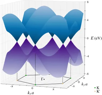
may be calculated using a tight-binding approach, following Wallace [3] and Castro Neto et al. [7]. Considering only nearest-neighbor hopping, i.e., A sites to B sites and vice versa, produces the dispersion relation
Ep⃗kq t
v u u
t1 4 cos
(√
3kxa
2
)
cos
(
kya
2
)
4 cos2
(
kya
2
)
(1.4)
Figure 1.2: Energy as a function of⃗kafor electron states (upper blue surface) and hole states (lower purple surface) in graphene. The two meet at the six Dirac points, labeledKorK1.
A low-energy approximation may be made by expanding equation 1.4 aroundKorK1 which yields3
E
(ÝÑ
ΓK ⃗q
)
t
√
3 4q
2 xa2
3 4q
2
ya2 t
√ 3a
2 |⃗q| (1.5)
with group velocity⃗v¯h1∇⃗qE(⃗q) ¯h1t
√
3a{2 ˆq. Thus, the low-energy dispersion is
Ep⃗qq ¯hvF|⃗q| (1.6)
where ¯h is Plank’s constant divided by2π andvF ¯h1t
√
3a{2 is the Fermi velocity, approx-imately 8105m/s. Note that, unlike in systems with a free-electron-like parabolic dispersion relation,vF does not depend on energy.Ep⃗qqis plotted on top ofEp⃗kqalongKK1in Figure 1.3.
3 Only terms under the radical with a total order inq
Figure 1.3: Low-energy dispersionEp⃗qq(equation 1.6) plotted alongKK1withEp⃗kq(equation 1.4) for comparison
1.1.2 Density of states
The density of states near the Dirac points may be calculated by adding up the states with energy¤
E. Given the rotational symmetry ofEp⃗qqthe available area ofk-space is
AkpEq π
( E ¯ hvF )2 . (1.7)
Eachk-state “occupies”p2π{Lq2ofk-space (whereLis the length of the sample) and has fourfold degeneracy due to spin and the two inequivalent Dirac points, so the number of states is
NpEq AkpEq
4 p2π{Lq2
L2 π ( E ¯ hvF )2 . (1.8)
Thus, the density of states per area of graphene is
DpEq 1 L2
dN dE
2|E| π¯h2v2
F
. (1.9)
1.1.3 Quantum capacitance
The commonly used expression for charge density in graphene placed near a gate electrode at volt-ageVg with geometrical capacitanceCg1 per unit area is
neCg1Vg (1.10)
which neglects the shift in Fermi level necessitated by graphene’s finite density of states. Taking this into account, the density isn∫08DpEqfpEF, TqdEwherefpEF, Tqis Fermi-Dirac distribution at temperatureT. AtT = 0, the density is
n 2 π¯h2v2
F
∫ EF
0
EdE 1 π ( EF ¯ hvF )2 (1.11) meaning that
EFpnq ¯hvF
√
πn. (1.12)
As an aside, equation 1.12 may be used calculate the shift in Fermi level for a known electron or hole concentration. Consider a graphene device equipped with a gate separated from the sheet by 300 nm of SiO2(ϵox= 3.9ϵ0). Applying the equation 1.10 withVg= 14 V yieldsn= 1012cm−2and
EF = 93 meV. Comparing this energy scale to the region of overlapping curves in Figure 1.3 lends support to the efficacy of the low-energy approximation.
The charge density may be determined in a self-consistent manner by separating the electrostatic and kinetic energies such that
eVg eϕ EF (1.13)
where ϕis the electrostatic potential of an electron on the graphene sheet. Substituting in equa-tion 1.12 andϕne{Cg1 and solving yields an improved version of equation 1.10 [12]:
neCg1Vgnqe
(√
1 2C
1 gVg
nqe
1
) nqe
πp¯hvFCg1q2
2e3 (1.14)
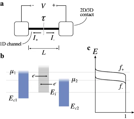
Figure 1.4: Schematic and band diagram of a 1D channel between 2D/3D contacts. (a) Circuit schematic showing virtual currents I andI. The channel includes a transmission coefficient
τ. (b) Band diagram of contact conduction bands and channel states. The right-moving electrons contribute to I and left-movers, toI. (c) Occupation functions for electrons injected into the channel. (Adapted from Datta [16].)
1.2
Conductance of a point contact
The conductance quantumG0 2e2{h, whereeis the electron charge andhis Plank’s constant, is common in mesoscopic physics such as the study of point contacts or one-dimensional (1D) con-ductors. Examples of the former include metallic break junctions [13] and gated constrictions in two-dimensional electron gases [14]. The latter include carbon nanotubes which support ballistic conduction over µm length scales and have different 1D sub-bands depending how they are “rolled-up”. Carbon nanotubes are not the only known carbon-based 1D conductors, however, given evi-dence for the existence of carbon-atom wires reported by Rinzler et al. in 1995 [15]. The quantized conductance of a single, spin-degenerate channel is derived below.
Figure 1.4a shows a model system comprising a channel between bulk (2D or 3D) contacts, to which a bias voltageV is applied. The energy of an electron traversing a one-dimensional channel of lengthLis
whereEpkqis the dispersion relation andEiis the band edge, which includes the additional energy arising from the lateral confinement of a particular mode i. Assuming the channel is a ballistic conductor save for a transmission coefficientτ ¤ 1, the right-moving electrons produce a virtual current
I ∑
k
nevf τ (1.16)
wherene2e{Lis the electron density perk-state (including spin degeneracy),v¯h1dE{dkis the group velocity, andf is the occupation function given the known chemical potentialµ1of the left-hand contact. A simple band diagram is shown in Figure 1.4b. Integrating overk-space yields:
I L 2π ∫ 8 0 2 Le 1 ¯ h dE
dkf τ dk 2e
h
∫ 8
Ei
f τ dE
Subtracting the equivalent expression for the left-moving electrons and dividing by V gives the conductance:
G I I V
2e h
e µ1µ2
∫ 8
Ei
(f f)τ dE (1.17)
Assumingτ is independent of energy andeV !kBT (f andfare shown for nonzero tem-perature in Figure 1.4c), the integral in equation 1.17 becomes(µ1µ2), giving a linear response conductance
G 2e
2
h τ. (1.18)
Note that this predicts a finite conductance for even highly transmitting channels resulting from the interface with the contacts [16]. This quantity is the conductance quantumG077.5 µS.
Chapter 2
Fabrication and measurement
techniques
2.1
Introduction
The graphene-based devices for this work were made using a combination of standard and propri-etary techniques. The basic formula included random deposition of graphene and/or graphite oxide onto silicon (covered by a layer of SiO2) substrates with predefined grids of alignment marks.
Care-fully designed source, drain, and, sometimes, top-gate electrodes were then created using electron-beam lithography (EBL) and either thermal or electron-electron-beam evaporation of metal followed by liftoff. These basic steps are described in detail along with alternative approaches to provide con-text and directions for future improvements.
2.2
Graphene deposition
The practical process of transferring a single graphene sheet from a bulk graphite source to a sub-strate is quite simple considering the late date (2004) at which is was first definitively demon-strated [1]. Several early methods are summarized:
Microcantelever cleavage
Arrays of µm-scale square graphite pillars are made at the surface of highly-oriented pyrolytic graphite (HOPG) by etching the surrounding material. Indi-vidual pillars are then detached and affixed to silicon microcantelevers using a precision micromanipulator. Finally, an atomic force microscope (AFM) is used to drag the pillars across a substrate, leaving a trail of thin1graphite layers [18].
Mechanical exfoliation
Large (20 µm–2 mm) graphite mesas prepared from HOPG via oxygen plasma etching are immobilized in photoresist. The mesas are then repeatedly thinned with adhesive tape before being released into an acetone suspension which is applied to a substrate [1].
Drawing Adhesive tape is used to cleave HOPG or Kish graphite,2exposing a fresh sur-face which is dragged across a substrate by hand. Occasionally, graphene’s strong interaction with the SiO2 surface [20, 21] causes sheets to be “pulled
out” of the bulk [22].
Both the drawing method and a variation of the mechanical exfoliation method (sometimes called the modified Scotch tape method) were used in this work. The latter seems to be the most com-monly used method at the present time: Adhesive tape removes a thick layer of graphite from the bulk, which is repeatedly cleaved by folding and unfolding the tape. The tape, now resembling a small, metallic-grey Rorschach test, is then placed directly on the substrate and slowly peeled off. With practice this method can reliably produce graphene sheets, although residual adhesive is a concern [23].
The drawing method, while cleaner than the modified Scotch tape method, can be finicky in practice. Optimizing factors such as cleaving rate, pressure, and drawing speed can be challenging and at times the process seems to be more art than science. There are several ways to promote the transfer process, such as electrostatic deposition, in which a bias is applied between the substrate and graphite source [24], or starting with expanded graphite [25]. Other improvements were explored such as thinning flakes on-chip by pressing and peeling PDMS (polydimethylsiloxane), sometimes leaving single sheets underneath. Low-power oxygen plasma was found to remove the top layer from multilayer sheets, although the process was not found to be controllable and may introduce defects.
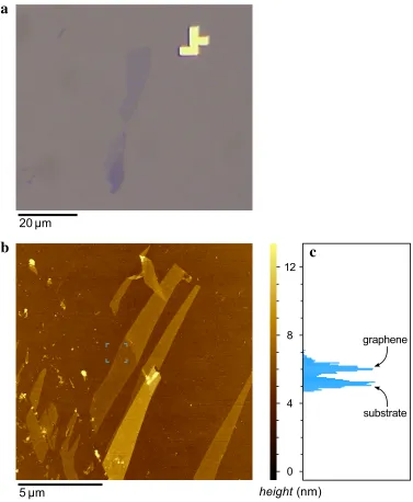
Figure 2.1: Micrographs of graphene on SiO2substrate. (a) Optical micrograph of graphene near a
metal alignment mark. (b) False color atomic force micrograph of graphene, with height scale bar at right. (c) Height histogram (with arbitrary units) generated from the area indicated by blue marks in (b). The peak spacing, a measure of the thickness of the sheet, is 0.9 nm.
spacing is 0.9 nm, suggesting that the graphene is a single layer. However, the measured substrate-to-graphene step height may vary with AFM tip sharpness and environmental conditions, making AFM an unreliable method of layer-counting. Indeed, measurements by two different tips on the
same sheet(not shown) produced values of 0.7 nm and 1.8 nm.
on nickel [28, 29] or copper [30]. While the carrier mobility of CVD graphene has improved, the traditional methods described above are still used for many experiments. Ironically, even some mobility-independent experiments benefit from starting with smaller sheets because no etching is then required to make space for electrodes.
2.3
Graphite oxidation
Graphite oxide (GO)3is graphene’s native oxide in the same sense that SiO2goes with silicon. The
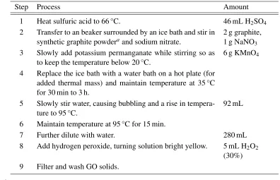
[image:26.612.92.488.405.660.2]GO used in this work was made by oxidizing synthetic graphite powder following the method of Hummers and Offeman [32] first reported in 1958. The process was scaled down and is summarized in Table 2.1. Temperature control proved challenging in practice (particularly during one nearly-disastrous early attempt), but nonetheless the resulting GO flakes had properties similar to those reported elsewhere [31, 33].
Table 2.1: Summary of modified Hummers method for oxidizing graphite
Step Process Amount
1 Heat sulfuric acid to 66C. 46 mL H2SO4
2 Transfer to an beaker surrounded by an ice bath and stir in synthetic graphite powderaand sodium nitrate.
2 g graphite, 1 g NaNO3
3 Slowly add potassium permanganate while stirring so as to keep the temperature below 20C.
6 g KMnO4
4 Replace the ice bath with a water bath on a hot plate (for added thermal mass) and maintain temperature at 35C for 30 min to 3 h.
5 Slowly stir water, causing bubbling and a rise in tempera-ture to 95C.
92 mL
6 Maintain temperature at 95C for 15 min.
7 Further dilute with water. 280 mL
8 Add hydrogen peroxide, turning solution bright yellow. 5 mL H2O2
(30%) 9 Filter and wash GO solids.
a
Sigma-Aldrich, 20 µm
3 The term graphite oxide is used throughout this work because most of the layers used were significantly thicker than the
2.4
Processing
Fabricating graphene-based devices using random deposition normally requires a set of custom metallic electrodes for each sample, although there are exceptions. For example, careful application of drawing method across a trench combined with predefined electrodes can produce a graphene device with no additional lithography [34]. However, the common method of using electron-beam lithography to define electrodes in reference to an alignment grid was used throughout this work:
1. Create a metallic alignment grid encompassing the majority of a0.5 cm Si/SiO2substrate.
2. Deposit graphene sheets using the drawing or modified Scotch tape method.
3. Locate one-to-few-layer sheets using optical microscopy and record reference micrographs.
4. Design a custom electrode pattern based on the locations of the sheets relative to the alignment grid.
5. Deposit metallic electrodes using electron-beam lithography and thermal or electron-beam evaporation followed by liftoff.
Steps one and two are sometimes reversed such that a only a small alignment grid is required given known regions of graphene sheets. Fortunately, a wafer-scale electron-beam pattern generator (Le-ica EBPG 5000) was available in the Kavli Nanoscience Institute cleanroom at Caltech, allowing many identical large-scale grids to be made at once. Thus, the fabrication process for each sam-ple really begins at step two, meaning that only a single additional lithography step is required. This lithography was most often run on a Hitachi S-4100 field-emission scanning electron micro-scope (SEM) located in Caltech’s Micro/Nano Fabrication Laboratory.
2.4.1 Electron-beam lithography
Electron-beam lithography using a converted scanning electron microscope offers rapid prototyping of devices with scales from 100s of µm down to50 nm with a minimum of substrate and pattern preparation. The standard recipe used in this work is listed in Table 2.2. The procedure is surpris-ingly tolerant of variation in its parameters with the exception of the electron exposure dose of step six.
Table 2.2: Typical electron-beam lithography process flow
Step Process Parameters
1 Heat substrate on hotplate to remove adsorbed water. 115C, 5 min 2 Spin on first layer of resist.a 4000 r/min, 45 s 3 Briefly prebake to set first layer of resist. 170C, 5 min 4 Spin on second layer of resist.a 4000 r/min, 45 s
5 Finish prebaking. 170C, 60 min
6 Expose pattern with electron beam. 30 keV, 300 µC/cm2
7 Develop pattern in 1:3 MIBK:IPA.b 50–60 s
a MicroChem NANO, first layer: MAA EL9, second layer: PMMA 950 C2.
b Methyl isobutyl ketone : isopropyl alcohol
across the entire substrate. Typically, the metal film comprises 40 nm of gold over a relatively thin chromium or titanium underlayer to aid adhesion. The PMMA is then dissolved in acetone to “lift off” the excess metal leaving only the metal that was in contact with the sample. The EBL, metallization, and liftoff processes are shown schematically in Figure 2.2a–e.
Alignment marks are made using a similar process as for electrodes. An extra isotropic etching4 of the oxide layer (Figure 2.2f) is inserted after EBL (Figure 2.2a–c) to recess the marks so they do not interfere with the drawing method. The MAA/PMMA bilayer is not necessarily resistant to acid-based etches, so a simple test on uniform layers was completed to verify the suitability of this process for noncritical features. The results, listed in Table 2.3, show noticeable loss of MAA while the PMMA is largely unaffected. As before, the metal marks are defined by shape of the PMMA windows (Figure 2.2g–h) so the additional undercut only serves to widen the small trenches at the edges of the marks.
Table 2.3: Initial film thicknesst0 and etching rate in 10:1 buffered oxide etch for PMMA, MAA, and SiO2
Material t0 ∆t(60 s) PMMA 1230 ˚A −50 ˚A
MAA 3710 ˚A −260 ˚A SiO2 2900 ˚A −500 ˚A
Figure 2.2: Electrode (a–e) and alignment mark (a–c, f–h) process flow. Vertical dimensions are to scale. (a) Substrate covered by bilayer MAA/PMMA resist. (b) Electron-beam exposed pattern. (c) Mask formed by development. (d) Cr/Au or Ti/Au metal film evaporated across entire substrate. (e) Electrode after liftoff. (f) Isotropically etched well. (g) Cr/Au or Ti/Au metal film evaporated across entire substrate. (h) Alignment mark flush with substrate surface
2.4.2 Alignment
50 nm pixel size of the alignment windows, it is worth considering the process in more detail to be
prepared in the event that problems do arise (and perhaps to have something to contemplate while the SEM is writing).
There are three coordinate systems — real spacex-y, pattern spacexp-yp, and writing spacexw
-yw— which may be rotated or skewed relative to one another.5 Here the predefined alignment marks and graphene (obviously) exist in real space while the electrode design, made in a computer-aided design (CAD) program, exists in pattern space. The two are related by
⃗rp Tm⃗r, (2.1)
where ⃗r is the real position of a feature and⃗rp is the equivalent location in the CAD program.
Tmdiffers slightly from the identity matrix depending on the calibration of the microscope used to
measure the existing features. Given a raw pattern, the SEM will reproduce it at the surface of the sample subject to systematic distortionTsdefined by
⃗
rwTs⃗rp, (2.2)
where⃗rw is awrittenfeature’s physical location.
In the simplest case, the goal of alignment is to makexw-yw overlay perfectly ontox-y.NPGS will calculate the optimal matrixTasuch that
⃗
rwTsTaTm⃗r ⃗r (2.3)
for the specified alignment points. The weakness of this approach may be demonstrated by consid-ering a poor microscope withTm I.6 A square shape in pattern space, while still guaranteed to
match the preexisting features, will become nonsquare in writing space.
The process may be improved by splitting the alignment into two parts, effectively findingTm
andTsindependently. Tm1 may then be applied to the pattern before loading it into NPGSsuch
5
Trivial origin offsets are ignored in this exposition. 6 The typical deviation ofT
mfromIdepends on the type of microscope. One would expect optical microscopes to have
thatTa Ts1. In practice the first alignment is performed by using image processing software
to match alignment marks with their known locations. This assumes that the alignment grid was written accurately to begin with, a safe assumption when using a dedicated EBPG for that step.
2.5
Electron transport measurements
Electron transport measurements must be matched to the energy scale and time scale of the phenom-ena being probed. The thermal energy scalekBTis 26 meV at 300 K and 121 µeV at 1.4 K, such that mV-scale DC biases are appropriate at room temperature while AC lock-in techniques are required a liquid helium temperatures. Switching measurements, on the other hand, require volt-scale biases with large bandwidth to capture ms- or µs-scale events. Three measurement setups common to the experiments in this work are described. Special attention to electrostatic discharge and grounding was paid throughout.
Current-voltage characteristics and gate voltage sweeps were recorded for many graphene de-vices at room temperature immediately after fabrication. These measurements were conducted in vacuum to minimize doping by adsorbed water vapor [36]. Vacuum conditions were also neces-sary for the electrical breakdown process described in chapter 3. The schematic for a typical setup is shown in Figure 2.3. A computer running custom software (Mezurit 2, described in detail in chapter 5) equipped with a National Instruments (NI) data acquisition (DAQ) card supplies a bias
Figure 2.3: Circuit schematic for room temperature DC measurement, in vacuum7
7
Mezurit 2implementsvirtual channels, making it easy to configure the DAQ card for any measurement. In this case, the three channels,X0,X1, andX2, are as shown below. Note that SI prefixes are handled automatically such that currentI
will be displayed in µA without needing to modifyX2.
Vb (V) X0DACp0,0q
Vbg (V) X1DACp0,1q 10
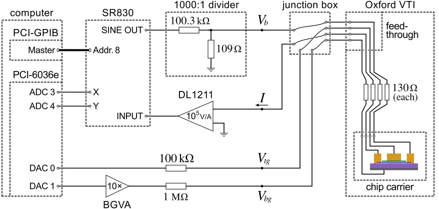
Figure 2.4: Circuit schematic for low-temperature AC measurement8
voltageVbto a two-terminal graphene device placed within a sealed, evacuated chamber through a junction box and electrical feed-through. The back-gate voltageVbg is supplied in proportion to a second analog output voltage by the custom bipolar gate voltage amplifier (BGVA) described in ap-pendix B. CurrentI is measured by a DL Instruments current preamplifier which outputs a voltage to be read on one of the DAQ card’s input ports.
Low-temperature measurements of linear response conductance were carried out in an Oxford Instruments variable temperature insert (VTI) using low-frequency AC lock-in techniques. The sample is such systems is cooled by evaporation of liquid helium flowing through a needle valve into the sample space, which is pumped down to 1 mbar. The circuit schematic is shown in Figure 2.4. In this case theVb is necessarily supplied by the Stanford Research Systems SR830 lock-in amplifier and the measured current response is transmitted to the DAQ card as analog voltages proportional to itsXandY components. The DC top-gate and back-gate voltagesVtgandVbg are supplied, as before, by the analog outputs of the DAQ card. The lock-in output level and input sensitivity are controlled byMezurit 2over a general purpose interface bus (GPIB) connection.
8 The virtual channels for this case are listed below. Note that GPIB functionsSR830 SineOutandSR830 SineOutand
SR830 SensInare bidirectional such that they may be set inMezurit 2or changed on the control panel of the lock-in.
Vb (µV) X0SR830 SineOutp0,8q 109{p109 100.3103q
Ix (nA) X1ADCp0,3q{10SR830 SensInp0,8q 105
Iy (nA) X2ADCp0,4q{10SR830 SensInp0,8q 105
Vtg (V) X3DACp0,0q
Chapter 3 describes bias-induced switching in graphene nanogaps on the order of 10−4s or faster. Capturing the switching process therefore requires faster data acquisition than the 0.1–1 kHz used for low-speed DC measurements. Mezurit 2is capable of recording points up to 1 MHz in “scope-mode” but is limited to kHz-scale waveform generation. Thus, an external instrument such as the Stanford Research Systems DS345 function generator is needed to apply high-quality waveforms to the device. The DS345 was chosen for its arbitrary waveform capability, which allows the user to supply a digital description of the desired output as a function of time. Pulse trains were defined in simple text files and converted into the necessary format using awcgen(usage instructions in appendix C) before being programmed into the DS345 over RS-232.
The measurement setup is shown in Figure 2.5. The DS345 is configured to wait for a signal via the TTL-compatible9 trigger input before running one cycle of the pulse train. On each run, Mezu-rit 2sends a 5 V trigger signal and simultaneously begins high-speed acquisition up to 100 kHz.10 The bias voltageVb is fed back to the DAQ card along with the measured currentI to produce a synchronized dataset.
Figure 2.5: Circuit schematic for higher-speed measurement11
9
TTL (transistor-transistor logic) allows voltage range of 0–5 V with 0–0.8 V defined as 0 and 2–5 V defined as 1. 10
The NI PCI-6036e is capable of 200 kS/s, so for two channels the maximum rate is 100 kHz. The DL 1211 is also a factor — its 3 dB bandwidth is 60 kHz at 103V/A and falls to 4 kHz at 109V/A [37].
11
The virtual channels for this case are listed below. Note that the trigger channel need not be saved to disk.
Vtrig (V) X0DACp0,0q
Vb (V) X1ADCp0,2q
2.6
Future work
Improvements to existing fabrication and measurement techniques are an integral part of nanoelec-tronics research. There is a trade-off, however, between automating and parallelizing these tech-niques and focusing on the Science, so to speak. In practice the appropriate balance can be hard to find and may shift as new techniques become available or drop in time or monetary cost. Several possible future directions are highlighted:
• Aligned layer transfer [38], while itself an involved process, offers more control and possibly better yield.
• The expanded use of CVD graphene and parallel fabrication methods including photolithog-raphy would produce a much greater number of devices per unit time. This would enable more robust statistics and in general larger experiments. For example, a greater breadth of functionalization methods for graphene sensors could be tested at once.
• Transport measurements could be automated to a degree approaching that of industrial para-metric test systems. A reasonable starting point would be a computer-controlled array of me-chanical relays to replace the standard manual junction box and preamplifiers with remotely adjustable gain.12
Chapter 3
Atomic-scale switching in graphene
nanogaps
3.1
Introduction
The ultimate limit for the miniaturization of electronics is the atomic scale. Reaching this limit will require novel materials as well as new paradigms for device operation and architecture. Graphene has rapidly emerged as an exceedingly promising novel electronic material [1, 10, 39, 40] for scaling beyond-complementary metal oxide semiconductor (CMOS) circuitry and architecture. Compared to silicon, graphene has far superior mobility [1, 39, 41–44], thermal conductivity [45] and current-carrying capabilities [46], and may support room temperature ballistic transport [10]; yet like sili-con, it has a planar geometry that enables multilayer device architecture and simplifies future inte-gration with CMOS technology. However, the absence of a band gap poses a major challenge for graphene electronics, as this limits the on/off ratio of digital devices. Recent progress has been made towards fabrication of graphene nanoribbon field effect transistors with high on/off ratios [47–49]; nevertheless, this approach presents several additional challenges such as precision control of the ribbon width and the atomic structure of the graphene edges. Switching behavior with high on/off ratio may also be promoted via chemical modification of graphene, though improvement in cycling capability remains to be developed [50].
for advanced lithographic techniques, similar to that employed in metallic wires [51, 52]. Applying appropriate bias voltage pulses switches the gap conductance between high (ON) or low (OFF) conductance states. Remarkably, these switches are extremely robust; they have operated for many thousands of cycles without degradation, with the conductance state easily persisting for greater than 24 hours, and perhaps indefinitely. As an example of potential applications, a prototype circuit was built to demonstrate information storage based on the combination of two or more switches using rank coding, in which information is stored by the relative magnitudes of device conductance in a memory cell. Such non-volatile, robust, atomic switches based on graphene, which are suitable for integration with CMOS as well as monolithic integration with graphene electronics, are promising as components for atomic-scale devices.
3.2
Device fabrication
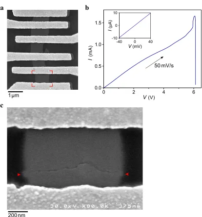
Two-terminal graphene devices are fabricated using standard techniques [22], as detailed in chap-ter 2. Briefly, graphene sheets are transferred from a high-quality graphite source1 to a heavilyp -doped silicon substrate with a 290 nm layer of thermally grown oxide. One- or two-layer graphene sheets are identified by color interference using optical microscopy, and then sorted by shape and size. Sheets which are roughly rectangular in shape and have a width of less than a few µm (to limit the required breakdown current) are made into devices by attaching metallic (Cr/Au or Ti/Au) leads using electron-beam lithography and thermal evaporation. No etching step is required given the prevalence of usable sheets produced by the graphene deposition process.2 Figure 3.1a shows
an electron micrograph of a completed sample containing five devices.
3.3
Measurements
The samples are placed within a vacuum chamber for room-temperature transport measurements, which is then evacuated to10−7Torr. High-vacuum conditions were found to be crucial to the breakdown process, presumably because this prevents atmospheric gases from reacting with the graphene.
1
Highly-oriented pyrolytic graphite, NT-MDT, grade ZYA or Kish graphite, Covalent Materials 2
Figure 3.1: Device images and nanogap formation for a single representative graphene device. (a) Electron micrograph of the sample before as-fabricated. The red markers indicate the specific device under test. (b) Current versus voltage during the electrical breakdown process. Inset: Low-biasI-V
characteristic prior to breakdown. (c) Electron micrograph of the area indicated by the red markers in (a), showing the device after breakdown. The red arrows indicate the ends of the nanoscale gap.
3.3.1 Electrical breakdown
current as measured by a DL Instruments 1211 current preamplifier.3 Figure 3.1 demonstrates the process for a single, representative device (identified by the red markers in part a). The baselineI-V
(Figure 3.1b, inset) demonstrates a before-breakdown conductance of250 µS. The breakdownI
-V is shown in Figure 3.1b. Starting from 0 V, the voltage is ramped up at a uniform rate of 50 mV/s. At a critical sheet current density of approximately 1.6 mA/µm, the measured current drops precip-itously, indicating breakdown of the graphene sheet. Interestingly, the conductanceI{V increases before breakdown, possibly due to current-driven annealing [53]. Figure 3.1c shows an electron mi-crograph of the device after breakdown, containing an distinct break across the graphene channel. Atomic force microscopy (AFM) confirms that a physical gap forms in the graphene. In the most narrow segments the gap’s width is typically less than 10 nm, although the precise location of the closest approach is difficult to determine due to the finite resolution of AFM. Thus, the device after breakdown includes a nanoscale junction between two physically separated sheets of graphene.
3.3.2 Junction conductance
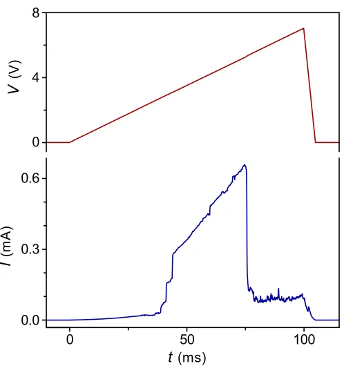
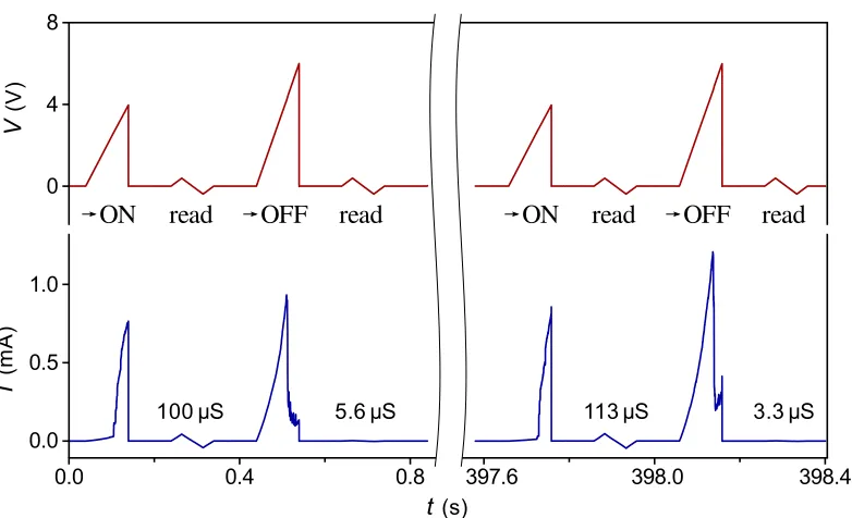
Following the breakdown step, the low-bias device conductance is much lower, ranging from0.1 nS to20 µS. Remarkably, this conductance can be reproducibly increased or decreased using addi-tional voltage pulses. Figure 3.2 illustrates a single cycle of such conductance modification applied to the same device. These data were obtained using a function generator to supply the voltage pulses combined with “scope-mode” data acquisition as described in chapter 2. The upper trace displays the applied source-drain biasV, which is quickly ramped up as a function of time, and the lower trace displays the current response. WhenV 2 V, the current is very low; when it reaches2.5– 4 V, the current abruptly increases, reaching a maximum of 0.65 mA up to 5 V. At still larger voltages, the device returns to its initial low-conductance state. The conductance exhibits little or no gate voltage dependence in either state. Thus, by applying voltages of different magnitudes, the graphene devices can be switched between relatively high-conductance, defined as “ON”, and low-conductance, defined as “OFF”, states, thereby functioning as voltage-programmable bistable switches or memory elements.
Figure 3.2: Switching behavior in a representative device. Applied junction voltage (upper trace) and junction current (lower trace) versus time for the device shown in Figure 3.1 after electrical breakdown, showing conductance recovery and subsequent reduction
Similar conductance switching has been observed in a number of systems, such as molecules [54], titanium oxides [55], and Ag/Ag2S nanowires [56]. What sets these graphene switches apart are
their unique combination of reproducibility, nonvolatility, and integrability with graphene electron-ics. The conductance state has been cycled up to 105times without degradation. Once the devices switch, they remain in either ON or OFF states for greater than 24 hours at room temperature, without external maintenance voltages. Although a systematic study of continuous monitoring for longer time periods has yet to be performed, device conductance values have remained similar to their last written states after several weeks.
Figure 3.3: Repeatable programming over hundreds of cycles. Upper trace: Voltage applied to the junction versus time. A ramp with a peak value of4 V corresponds to a turn-on pulse, while a ramp with a peak value of6 V corresponds to a turn-off pulse. A small, sawtooth-shaped readout pulse is applied after each write to determine the low-bias junction conductance. Lower trace: Current flow through the junction, with the extracted low-bias conductance labeled above each readout pulse
states, although similar current levels flow during the writing process. The ON state conductance is typically100 µS, while the OFF state conductance is typically5 µS. The right-hand section of the plot shows data from the end of the measurement, which comprised500 switching cycles. The device behavior is virtually identical to that shown on the first cycle, demonstrating exceptional reproducibility.
3.3.3 Time-resolved switching
To gain further insight into the switching mechanism, the time-resolved transition from the OFF to ON state was captured, again using a function generator and “scope-mode” data acquisition. The voltageV was quickly increased while monitoring the current, as in Figure 3.2. In this case, the conductanceI{V is plotted versusV for the voltage range where switching normally occurs (Fig-ure 3.4a). The plot shows well-defined steps inI{V, with magnitude G0. These characteristic step sizes, which include a series resistance from the graphene sheets, can vary by factor of order unity from device to device. HereG0 2e2{h, the conductance quantum, whereeis the electron charge, andh is Planck’s constant. SinceG0 is the conductance of a spin-degenerate one dimen-sional conductor, e.g., a linear chain of gold atoms [13], observation of these steps suggests that the device conductance states are likely multiples of highly transmitting quantum channels.
These data were recorded using a 10 kHz sampling rate to attempt to capture the switching pro-cess. Although for technical reasons4it is difficult to visualize the time scale of the switching in Figure 3.4a, careful inspection of the raw data (not shown) reveals that the conductance value tran-sitions between the step plateaus in no longer than 2–310−4s. The actual transition is probably
Figure 3.4: Conductance steps and histogram of conductance during switching. (a) Conductance
I{V versus biasV recorded while the device switches from the OFF to ON state. A sequence of steps of magnitude2e2{hare observed. (b) Histogram of conductance values showing two major peaks at approximately integer multiples of2e2{h
4 Both the voltage and current are recorded as a function of time. When a transition occurs, the increased current causes a
faster still; the time resolution of this measurement is limited by the bandwidth of the hardware.
To further investigate this phenomenon, a histogram of the conductance was assembled from 1000 cycles, shown in Figure 3.4b. The histogram exhibits two main peaks, separated by2e2{h. These well-defined peaks, as well as the conductance steps, strongly resemble those found in the breaking process of mechanically controlled break junctions [13, 57], in which a linear chain of atoms forms between two closely spaced metallic electrodes. These results strongly suggest that the conducting pathway bridging the graphene edges is atomic in scale.
3.3.4 Switching rate
Additional information about the switching mechanism is provided by the voltage dependence of the switching rate. A square pulse with a given voltage magnitude is applied to the device in the OFF state, and waiting timet, defined as the time elapsed before the first sharp increase in conductance, is recorded. Because of the stochastic nature of the switching, tfollows a statistical distribution. Data from approximately 800 switching cycles were compiled into histograms. The upper panel in Figure 3.5a shows a histogram of the measuredtatV = 2.8 V. The peak att200 ms indicates the most probable time scale at which switching occurs. The lower panel shows similar data, but with a larger biasV = 3.4 V. The peak in probability distribution visibly shifts towards zero, indicating the high probability of switching at relatively short time scales. Moreover, these observed switching rates are found to be strongly temperature dependent, increasing by a factor of3 for every 10 K increase in temperature.
The strong temperature and voltage dependence indicates a thermally activated process. In the simplest picture, such a process can be described by a single rate
Γνe∆pVq{kBT, (3.1)
Figure 3.5: Statistical analysis of the switching dynamics and schematic of nanogap ON and OFF states. (a) Histograms of waiting times for the first conductance-increase step for two different bias voltages. (b) Proposed schematic atomic configurations in the ON and OFF states
3.4
Carbon chain model
rateΓ1; the second step is the binding of the chain which extends all the way across the gap, with rateΓ2. Both these rates should have a similar form to equation 3.1. The distributionPptqfor the total waiting time would then be given by the convolution of the waiting time for ann-step Poisson process with rateΓ1, known as the Erlang distribution, and a Poisson process with rateΓ2. Thus,
Pptq Γ
n 1Γ2
pΓ1Γ2qn
eΓ2t
n
∑
m1
Γn1Γ2
pm1q!t
m1eΓ1t 1
pΓ1Γ2qnm 1
. (3.2)
Fitting equation 3.2 to the data shown in Figure 3.5a givesΓ1= 51 s−1,Γ2= 3.6 s−1for the upper panel, andΓ1 = 4300 s−1,Γ2= 13 s−1for the lower panel. A value ofn= 5 was assumed based on the nm-scale gaps observed, which corresponds to a1 nm long carbon chain. The quality of the fit was not sensitive to the precise value ofn, which indicates considerable uncertainty in the value ofΓ1. Nevertheless, the time constants observed are consistent with eV-scale energy barriers.
This model of extending carbon chains coherently and comprehensively accounts for all the ex-perimental observations: the lack of gate dependence on conductance, the2e2{hconductance steps, as well as the voltage and temperature dependence of waiting time distribution. Taken together, the results strongly suggest that the devices switch by the formation and breaking of chains of carbon atoms; the conductance state of the device therefore changes by the motion of atoms rather than by electric charge. In addition, since the initial publication of these results [61] other workers5 have demonstrated similar switching behavior in nanogaps made fromsuspendedgraphene devices [62]. Although their results differ in some ways from those presented here, they do indicate that a nearby substrate is not an essential feature of a graphene-based switch.
3.5
Application to logic circuits
The properties of these junctions can be exploited to make logic gates and store information. How-ever, one potential obstacle is the relatively modest on/off ratio ( 100), while 105–106is typically achieved in CMOS devices. The distributions of conductance for the OFF and ON states was mea-sured by applying 4000 8 V square OFF pulses and 4000 4 V square ON pulses, each 100 ms long,
Figure 3.6: Low-bias junction conductance measured immediately after ON and OFF pulses. The left-hand axis applies to the OFF state distribution and the right-hand axis applies to the ON state distribution. The relative scales are adjusted for clarity given the different bin sizes of the two histograms (area as probability density is not directly comparable).
to a device in an alternating fashion. The low-bias conductance was measured after each writing pulse, and the results were compiled into histograms, shown in Figure 3.6. The maximum values of the two distributions lie 66 µS apart, but there is no significant separation between the tails. Thus, a graphene switch as a single memory element would have little noise margin. In addition, there is a small overlap in the 15 µS region which corresponds to a 0.5 % error rate.
3.5.1 Rank coding
One alternative approach is to utilize a novel memory cell based on rank coding [63]. A bit is stored not by the absolute value of the device conductance but by the comparison of the conductance of two or more devices in a cell. The information capacity for anN device cell is thereforelog2pN!q
bits, which, for largeN, exceeds even that of a conventional memory cell.
Figure 3.7: Circuit diagram of rank-coded cell
one of the write lines is connected through a multiplexer6 to a voltage source, labeledVw1 orVw2 depending on the selected device. During the readout phase, write lines are left floating6 while voltagesVo1andVo2on the readout lines are recorded. In this way, the conductance states of the two devices can be inferred from their respective readout voltagesVor1,2s=VRRr1,2s{pRr1,2s 200 kΩq, where R1 is the resistance of G1 and R2 is the resistance of G2, without the need for complex current-measuring circuitry. A schematic of the device circuit is shown in Figure 3.7.
The logical valueXof the cell is defined by the relative conductance of the two devices:
X
0 ifVo1 Vo2
1 ifVo1 ¡Vo2 undef. else
(3.3)
[image:46.612.184.392.69.274.2]The readout voltages may be sent to a comparator to encodeXas a digital logic-compatible voltage, or, as in this proof-of-concept demonstration, plotted and compared visually.
Figure 3.8a demonstrates the operation of the memory cell. The top three traces plot input voltagesVw1,Vw2, andVRversus time, while the bottom panel shows the readout voltages for both devices. The RCC demonstration begins with G2 in a more conductive state than G1 such thatVo2is “pulled” lower thanVo1, corresponding toX= 1. VoltageVRis then decreased to zero, after which
6
Figure 3.8: Demonstration of operation and retention time for the rank-coded cell described in Figure 3.7. (a) Write and read-out voltages versus time. Top two traces: Voltages applied to the write lines of device G1 and G2. Third trace: Readout excitation voltage. Bottom traces: Readout voltage for devices G1 (blue) and G2 (green). The logical stateXis indicated above each readout. (b) Readout voltage versus time over a 24 hour period with no write voltages applied
a turn-on pulse is applied to G1, increasing its conductance such thatVo1 Vo2, flipping value of the memory bit. After another readout cycle to confirm the state of the RCC, a turn-on pulse is then applied to G2, which increases its conductance beyond that of G1,7switchingX back to1. Thus, the logical state of the RCC has been switched from 1 to 0 and back to 1 again.
7 A slightly larger turn-on pulse is applied to G2 to promote increased conductance, ensuring that its conductance
In principle, the sequence above could be continued indefinitely by applying turn-off write pulses to reset G1 and G2 to their original low-conductance states. This could be completed one device at a time such thatXeither retains its value or not, depending on the desired outcome. Given the stochastic nature of the switching in graphene nanogaps, a more-robust RCC may require a controller circuit that readsX after each write to confirm that the turn-on or turn-off pulse had the intended effect. The stability of the stored information is demonstrated in Figure 3.8b, which shows the voltage on the two outputs read continuously for 24 hours, without voltages applied on the write lines. The voltage rank is maintained during the observation time, indicating the stability of the stored bit for extended time periods.
3.5.2 Switching energy
One important metric of a digital memory technology is the switching energyQsw required to flip one bit. This value can be roughly estimated by assuming a square writing pulse of heightVswand widthγtsw, wheretswis the characteristic time before switching andγis a safety factor. The safety factor is necessary to accommodate the tail of the distribution oftswgiven the stochastic nature of the process, as illustrated for the OFF to ON transition in section 3.3.4. Given known preswitching currentI1and postswitching currentI2, the switching energy is
Qsw Vswtsw[I1 pγ1qI2]. (3.4)
Using typical values observed in the data used to generate Figure 3.6 and γ = 5 yields 70 µJ (3 µJ forγ = 1) when switching from OFF to ON8 and 6 µJ (3 µJ forγ = 1) when switching from ON to OFF.9These values are significantly higher than for other recent architectures, for example 0.7 pJ in TiO2resistive memory [64], but may be greatly reduced in future work. Possible avenues of
exploration include high-frequency ON pulses, higher-voltage OFF pulses, and intelligent controller circuits which adapt the writing voltage pulse to the device.
8 OFFÑON:V
sw= 4 V,tsw= 10 ms,I1= 80 µA,I2= 400 µA.
9 ONÑOFF:V
3.6
Future work
Chapter 4
Graphite oxide gate dielectric for
field-effect transistors
4.1
Introduction
Graphene’s excellent electronic, thermal, and mechanical properties make it an exciting novel ma-terial for many applications. Finding a compatible dielectric mama-terial remains a challenge due to graphene’s sensitivity to environmental conditions, including doping and charge disorder. While significant progress has been made in adapting bulk insulators including Al2O3[67, 68], HfO2[69–
71], and lead zirconate titanate (PZT) [72], the use of layered materials is just beginning to be ex-plored, for example, in carbon nanotube-graphite oxide-metal transistors [73] and graphene-boron nitride-metal transistors [74, 75]. Graphite oxide (GO) is of particular interest because it is com-patible with solution-based processing and deposition [31, 76]. In addition, compared to boron nitride, GO has the added benefit of being graphene’s native oxide, analogous to to silicon’s na-tive oxide, SiO2. Like SiO2, GO can be made from its parent material via oxidation [31], or by
local oxidation [77], and is an electrical insulator. This correspondence suggests the possibility of a novel all-graphene-based field-effect transistor built with a graphene channel, graphite oxide gate dielectric, and graphene top-gate.
and breakdown electric field comparable to SiO2, typically1–3108V/m. Comparing the gate efficiency of the back and top-gates gives an estimated relative dielectric constant approximately equal to SiO2, κ 4.3. The successful operation of these devices demonstrates graphite oxide’s
utility as a layered insulator for graphene circuits which could be used in a multitude of configura-tions. This shows the promise of GO for use in future all-carbon circuits, which could be used for flexible electronics.
4.2
Device fabrication
Graphene-graphite oxide field-effect transistors (G-GO FETs) are fabricated by random deposition, as illustrated in Figure 4.1, using the techniques described in chapter 2. First, graphene sheets are deposited by mechanical exfoliation [22] onto a heavilyp-doped silicon substrate capped with a 290 nm layer of thermally grown oxide. Next, graphite oxide flakes are made by oxidizing graphite powder,1 following the Hummers method [32] as described in section 2.3. The graphite oxide flakes are then mixed with deionized water to form a suspension with concentration 1 mg/mL, which is stirred for at least one day to exfoliate the flakes into thin sheets. Stirring produces larger, thicker sheets than ultrasonication. The graphite oxide sheets are then deposited randomly onto the substrates [31, 33, 78] using a “drop-and-dry” method.
Overlapping regions of one-to-few-layer graphene and one-to-multilayer graphite oxide sheets are identified using optical microscopy. An example region is shown in Figure 4.2a. Note the purple color of the underlying graphene, which can be seen through the green-tinted graphite oxide.
4.2.1 Electrostatic force microscopy
The geometry can be confirmed using electrostatic force microscopy (EFM) [79–81], which gives a qualitative measure of the local conductivity at the surface of a sample [82, 83]. EFM is performed by scanning a mechanically oscillating probe tip over the sample at constant (time) average height2 while a constant voltage bias is applied between the tip and sample. When the tip is located over a conductive region of the sample, the charge on the tip causes an image charge to form at the surface 1
Sigma-Aldrich graphite powder, 20 µm, synthetic
2 Knowledge of the local topography is needed to maintain a constant height. This information is determined by
Figure 4.1: Graphene-graphite oxide process flow (not to scale). (a) Graphene is deposited onto an oxidized Si wafer (violet). (b) Graphite oxide is then deposited from an aqueous solution. (c) Metal source, drain, and top-gate contacts are then deposited using electron beam lithography and electron beam evaporation. In practice, bilayer resist (not shown for clarity)