Thesis by
Su-Peng Yu
In Partial Fulfillment of the Requirements for the
degree of
Doctor of Philosophy
CALIFORNIA INSTITUTE OF TECHNOLOGY
Pasadena, California
2017
© 2017
Su-Peng Yu
ORCID: 0000-0003-1348-7447
ACKNOWLEDGEMENTS
I would like to acknowledge with sincere gratitude the collaboration and support
from my friends and colleagues that had made this project possible: My advisor,
Prof. Jeff Kimble, has always been supportive to my work and my various crazy
ideas. I’d also like to acknowledge Prof. Oskar Painter for the resources and
effort he provided for this collaboration between atoms and photonics. Chen-Lung
Hung, who motivated many of our efforts; Michael Martin, who is great with both
optics and electronics; Jae-Hoon Lee, with his attention to the details; Mingwu
Lu, who is knowledgeable and never hesitant to share; Alex Burgers, with whom
working is never boring; Dalziel Wilson, who inspired my interest in machining;
Akihisa Goban, who seems to get anything working in a breeze; Jonathan Hood
and Andrew McClung, with whom I cooked various chemicals together that were
often both poisonous and corrosive; Juan Muniz, who traps atoms and also makes
the best barbecue; Lucas Peng, whose programming skill allowed our project better
analysis; and Xingsheng Luan, whose photonic designs are even crazier than mine. I
would also like to acknowledge the people who helped me a lot in the Painter group:
Richard Norte and Justin Cohen, who taught me how to do nano-fab; and Sean
Meenehan, who is known for great simulation skills and appetite for coffee. I’d like
to acknowledge the work of our theoretical collaborators, Prof. Darrick Chang, who
answers every question with clarity and patience; and Ana Asenjo-Garcia, who is
always around for a fruitful discussion. Finally, I’d like to offer my thanks to Barry
Baker for keeping the cleanroom clean and well-supplied, Guy DeRose for keeping
the lithography machine always up and running, and Scott Curtis for keeping track
ABSTRACT
Development of technology can allow access to new regimes in science and creation
of new fields of research. The development of ultra-high finesse mirror technology
enabled the development of the field of cavity quantum electrodynamics, and an
abundance of wonderful physics experiments soon followed. The sophistication
of the field of nano-fabrication and nano-photonics would allow unprecedented
capability to mold the shape and flow of light, and provide a novel platform for
efficient and hopefully integrable quantum systems. In this project, we hope to
interface cold atoms, perhaps the most quintessential of quantum systems, to the
engineering power of nano-photonics. We believe this field of study will not only
lead to the demonstration of new physics in the quantum regime, but work toward
building a network with quantum capabilities mediated by optical channels.
In this project, we develop a fabricated platform capable of interfacing
nano-photonic devices with cold Cesium atoms in free-space. Nano-nano-photonic waveguide
devices are fabricated in a Silicon Nitride device layer on Silicon substrate. The
fabrication is compatible with conventional semiconductor fabrication processes,
and the chip design has been adapted to allow incorporation with free-space optics
to support cold Cesium atom cloud around the waveguides. An ultra-high vacuum
system that is compatible to the chip and its supporting structures was constructed
to perform experiments.
With our system, we were able to fabricate and characterize nano-photonic
struc-tures, including 1D photonic crystal waveguides, cavities, and 2D photonic crystal
slabs. For the 1D photonic crystal waveguide devices, enhanced atom-light coupling
between localized Cesium atoms in the vicinity of the devices, and also atom-atom
interaction between Cesium atoms mediated by the guided mode of the photonic
crystal waveguide, has been observed. The 2D photonic devices allow us many
capabilities beyond that of the 1D waveguide. Demonstration of exotic optical
prop-erties including natural decay rate suppression and circular polarization engineering,
PUBLISHED CONTENT AND CONTRIBUTIONS
S.-P. Yu et al. “Nanowire Photonic Crystal Waveguides for Single-Atom Trapping
and Strong Light-Matter Interactions”. In: Applied Physics Letters104 (2014), p.
111103. DOI: 10.1063/1.4868975
A. Goban et al. “Atom–Light Interactions in Photonic Crystals”. In: Nature Communications5 (2014), p. 3808. DOI: 10.1038/ncomms4808.
A. Goban et al. “Superradiance for Atoms Trapped along a Photonic Crystal
Waveguide”. In: Physical Review Letters 115 (2015), p. 063601. DOI: 10.
1103/PhysRevLett.115.063601.
J. D. Hood et al. “Atom–Atom Interactions Around the Band Edge of a Photonic
Crystal Waveguide”. In: Proccedings to National Academy of Science 113.38
(2016), pp. 10507–10512. DOI: 10.1073/pnas.1603788113.
The project of atom-light interaction with nanophotonic devices was made possible
only by the combined effort of all members of Prof. Kimble’s group, and the
collaboration with Prof. Painter’s group. My role in this project includes: simulation
and device design, in collaboration with Juan Muniz, and Sean Meenehan; the
developing of fabrication process and the fabrication of the devices, in collaboration
with Jonathan Hood, Andrew McClung, Richard Norte, and Justin Cohen; the
optical characterization of the devices and the developing of the chip-fiber assembly
design, which was a joint effort with Jonathan Hood and Michael Martin. All these
made the results in Yu et al. (2014) possible. I worked intermittently with the
atom measurement lab, with Akihisa Goban, Jonathan Hood, Chen-Lung Hung,
and Mingwu Lu. It was primarily their work that produced the results in Goban
et al. (2014), Goban et al. (2015), and Hood et al. (2016). My work for these
experiments were mostly with the building of the devices, and perhaps some minor
TABLE OF CONTENTS
Acknowledgements . . . iii
Abstract . . . iv
Published Content and Contributions . . . v
Table of Contents . . . vi
List of Illustrations . . . x
List of Tables . . . xiii
Chapter I: Motivation . . . 1
1.1 Nanophotnics and Optical Property Engineering . . . 1
1.2 Light Interaction with Quantum Emitters . . . 1
Achieving strong coupling to quantum emitter . . . 2
Light-mediated emitter interactions . . . 2
Emitter-mediated light interactions . . . 3
1.3 Interfacing Hybrid Systems . . . 3
Quantum networks . . . 3
1.4 Thesis Outline . . . 4
Chapter II: Support Structure Design . . . 6
2.1 Design Targets for Atom-Nanophotonics Hybrid System . . . 6
Chip layout to allow optical access . . . 6
Power handling . . . 7
Vacuum compatibility . . . 7
2.2 High-Stress Silicon Nitride and Mechanical Stress Handling . . . 8
Avoiding stress concentration . . . 8
Stress balancing to prevent deformation . . . 9
2.3 Thermal Conductance Structures . . . 9
2.4 Connecting Waveguides to Outside World . . . 11
FEM calculation and mode projection . . . 12
Direct time-domain simulation . . . 13
2.5 Anti-Reflection Designs on Highly Evanescent Waveguides . . . 14
’Round-about’ anti-reflection tether junction . . . 15
Y-shaped free-space coupling tether design . . . 17
2.6 Assembly of Fiber-Coupled Chip . . . 17
Notes on using glue . . . 18
Fiber feedthrough and strain handling . . . 19
2.7 Coupling into Free-Space Lens-Coupled Chip . . . 20
Chip configuration adaption to allow free-space coupling . . . 21
Vacuum and optics system consideration . . . 22
Chapter III: Fabrication of Devices . . . 24
3.1 Fabrication Requirements . . . 24
Device footprint and throughput . . . 25
Issues associated with wet chemistry processes . . . 25
3.2 Substrate Selection and Preparation . . . 27
Pre-patterning the backside for through-window etch . . . 28
3.3 Electron Beam Lithography with Large Device Footprint . . . 28
Coarse-fine double exposure . . . 29
Back-scattering electron . . . 29
Main-field stitching . . . 31
3.4 Etching . . . 32
Plasma etching for pattern transfer . . . 32
Directional wet etching of Silicon substrate . . . 33
3.5 Applications of Silicon Anisotropic Etching . . . 34
Etch-in of positive corners . . . 35
’Fuse’ timing method for residual Silicon control . . . 35
Silicon half-aperture for stray-light protection . . . 37
Etched precision cleave grooves . . . 38
Substrate rotation check patterns . . . 39
3.6 Wet-Chemistry Processing . . . 40
Chemical processing holder design . . . 41
Chip installation onto the holder . . . 42
Etching of the through-window . . . 42
Device chemical cleaning . . . 43
Device drying and surface tension . . . 44
Manipulation of devices using SEM charging effect . . . 45
3.7 Post-Release Plasma Cleaning . . . 46
3.8 Characterization using photonic crystal cavities . . . 47
3.9 Metal Deposition for Potential Electrostatic Tuning . . . 48
3.10 Device Fine-Tuning Using Atomic Layer Deposition . . . 49
3.11 Experiments with High-Temperature Annealing . . . 50
Thermal treatment to improve yield . . . 50
Post-release annealing . . . 50
Chapter IV: Engineering Optical Properties with APCW . . . 52
4.1 Engineering Atom-Light Coupling Using Photonic Crystal . . . 52
Mode profile of the photonic crystal waveguide . . . 53
Coupling enhancement on band-edges . . . 53
4.2 Placement of Photonic Crystal Frequency . . . 56
FDTD simulation and Green’s function . . . 56
4.3 Tapering Photonic Crystal Waveguides . . . 57
Envelop from residual taper reflection . . . 58
Phase-matched taper design . . . 58
4.4 Cesium Dual-Frequency Operation . . . 60
Alignment of PhC frequencies to Cs D1 and D2 lines . . . 60
Two-mode trap-and-probe scheme . . . 60
Side-illumination trapping scheme . . . 61
’TM’ modes . . . 62
Anti-symmetric modes . . . 63
Circular polarization engineering . . . 63
Chapter V: Optical Characterization of Devices . . . 68
5.1 Reflection and Transmission Measurement . . . 68
Light sources and analysis tool . . . 68
Polarization alignment . . . 69
Measurement using cleaved fiber-end . . . 70
Measurement using free-space optics with cleaved chips . . . 71
5.2 Features of Measured Spectra . . . 73
Power level and band-gap alignment . . . 73
Band-edge resonance regularity and quality . . . 73
Residual transmission through the band-gap . . . 74
5.3 Interaction Enhancement Estimation . . . 74
Using free spectral range of resonances . . . 75
Using scattering measurement . . . 76
5.4 Power Handling Capability Test in Vacuum . . . 76
5.5 Precision shifting to Cs frequencies using optical measurement feed-back . . . 77
5.6 Characterization of Single-Beam Fabry-Perot-Type Cavity . . . 77
Separation of propagation and mirror loss . . . 78
Reachable parameters and potential for cavity QED experiments . . 78
Chapter VI: Atom-Light Interaction Measurement . . . 85
6.1 Vacuum System Adaption for Photonic Devices . . . 85
Background pressure of Cesium . . . 85
Limitation associated with interfacing chip to outside optics . . . 86
Replacement of chips in vacuum chamber . . . 86
6.2 Vacuum System Design and Atom Delivery . . . 86
Dual-chamber design with atom ’faucet’ . . . 87
Atom collecting and delivery in the ’Science’ chamber . . . 88
6.3 Methods for Measurement of Atom-Light Interaction . . . 89
Frequency domain spectroscopy measurement . . . 89
Time-domain decay rate measurement . . . 90
6.4 Observation of Enhanced Single-Atom Decay Rate . . . 91
Results . . . 91
Discussion . . . 92
6.5 Observation of Light-Mediated Atom-Atom Interaction . . . 92
Result: Superradiance . . . 93
Result: Band-gap mediated interaction . . . 93
Discussion . . . 95
Chapter VII: Engineering Optical Properties with 2D Photonic Crystal Slabs . 97 7.1 Adaptation of Support Structures to Photonic Crystal Slabs . . . 97
Mechanical deformation of the 2D structure . . . 97
Coupling 2D structures to input waveguide . . . 98
TE bandgap and free-space decay suppression . . . 98
Dual-frequency directional emission . . . 99
Circular modes at K point air band . . . 100
Atom trapping in the 2D lattice hole . . . 100
7.3 Optical Properties of 2D PhC with Defects . . . 101
Point-defect super-suppressor . . . 101
1D defect slot waveguide . . . 101
7.4 Atom-Light Interaction Parameters of the Slot Waveguide . . . 102
Tapering Into the Slot Waveguide . . . 102
Anti-symmetric mode . . . 103
Green’s function and state-dependent atom response . . . 103
7.5 Characterization and Tuning of 2D-Based Devices . . . 104
Chapter VIII: Outlook . . . 116
8.1 Migration Toward Free-Space Coupled Devices . . . 116
8.2 Deterministic Loading and Positioning with Optical Tweezers . . . . 117
8.3 Electro-capacitive dynamic tuning of slot waveguide . . . 117
8.4 Potential Future Development . . . 117
Circular Polarization Engineering . . . 118
Multi-port devices . . . 119
Potential for ’random-access’ quantum system . . . 120
Bibliography . . . 122
Appendix A: FEM Simulation Methods . . . 128
A.1 Optical Band Structures . . . 129
Geometry and boundary conditions . . . 129
Meshing and solving . . . 129
Information output . . . 130
A.2 Mechanical stress and resonance frequency . . . 130
Geometry and boundary conditions . . . 130
Meshing and solving . . . 131
Information output . . . 131
Appendix B: FDTD Simulation Methods . . . 132
B.1 Transmission and Reflection . . . 133
Source placement . . . 133
Monitor placement . . . 133
Field projection into guided mode . . . 133
Data analysis and application . . . 134
B.2 Green’s Function Calculation . . . 134
Source placement . . . 134
Monitor placement . . . 134
Data analysis and application . . . 135
Appendix C: Dimensions for Chemistry Processing Holder . . . 136
LIST OF ILLUSTRATIONS
Number Page
1.1 Conceptual illustration of the Quantum Internet . . . 4
2.1 Suspension of large, hundred-µm scale strutures . . . 8
2.2 Geometries that create local heightened stress . . . 10
2.3 Tensile versus compressive corners . . . 10
2.4 Mechanical design to handle deformation . . . 11
2.5 Angled tether array for force balancing . . . 12
2.6 Waveguide and cooling rail . . . 13
2.7 Coupling waveguide mode projection into Gaussian beam profile . . 14
2.8 FDTD simulation plot of free-standing coupling waveguide . . . 14
2.9 Reflection from coupling waveguide support tethers . . . 15
2.10 Concept of hole-based dipole cancelation tether . . . 16
2.11 Dipole cancellation by tilted tethers . . . 18
2.12 Angled tether design field plot . . . 19
2.13 Fiber placement and automated glue application setup . . . 21
2.14 Chip holder assembly with fibers . . . 22
2.15 Free-space direct-coupling test setup . . . 23
3.1 Preliminary exploratory photonic crystals . . . 26
3.2 Stitching error . . . 27
3.3 Illustration of coarse-and-fine exposure with overlap area . . . 30
3.4 Slice-grid method . . . 31
3.5 Exposure and etch test patterns . . . 34
3.6 Illustration of anisotropic etching of Silicon substrate . . . 35
3.7 Full view of through-window chip and V-grooves . . . 36
3.8 Fuse-protected positive angles . . . 37
3.9 Silicon half-barrier formed by timed etching . . . 38
3.10 Illustration of chip cleaving by fabricated cleave groove . . . 40
3.11 Rotation check pattern . . . 41
3.12 Teflon chip holder for wet chemistry processing . . . 43
3.13 Congregate of solid contaminant removed by Hydrofluoric acid . . . 45
3.15 Re-condensation of organic material due to environmental
contami-nation . . . 47
3.16 Single-beam photonic crystal mirror . . . 48
3.17 Signs of potential thermal damage to silicon substrate . . . 51
4.1 Mode profile and band structure of the ’Alligator’ photonic crystal waveguide . . . 54
4.2 Formation of 1D band structure from waveguide dispersion curves . . 55
4.3 FDTD calculation of field profile and Green’s function . . . 59
4.4 Residual cavity induced resonances near band-edge . . . 64
4.5 Dipole trapping potential and Casimir-Polder forces . . . 65
4.6 Atom trapping using side-illumination . . . 65
4.7 TM mode profile at band-edge . . . 66
4.8 Shifted APCW to create very flat dispersion curve . . . 66
4.9 Systematic engineering of circularly polarized ’pockets’ . . . 67
5.1 Residual reflection and interference fringes of different coupler designs 69 5.2 Optical image of coupling waveguide tether junction scattering . . . . 70
5.3 Illustration of the characterization setup . . . 71
5.4 Optical image of coupling of device using free-space optics . . . 72
5.5 Features of a device in reflection and transmission measurement . . . 75
5.6 Analysis of band-edge resonances using simple cavity model with quadratic dispersion . . . 80
5.7 Features of a device in reflection and transmission measurement . . . 81
5.8 Device damaged in vacuum chamber . . . 81
5.9 Shifting the band edges using ALD coating . . . 82
5.10 Shifting the Nitride coupling waveguide optimal for 10nm ALD coating 83 5.11 Optical properties of the single-beam Fabry-Perot-type cavity . . . . 84
6.1 Illustration of vacuum system . . . 87
6.2 Illustration of Experiment Cycle . . . 90
6.3 Simulated distribution of Cesium atom near device . . . 92
6.4 Measurements of superradiance in number-dependent decay . . . 94
6.5 Measurements of Off-Resonance and Band-Gap Spectra . . . 95
7.1 Mechanical support frame and tension redistribution tethering . . . . 105
7.2 Band structure and mode profile for TE modes of 2D photonic crystal 106 7.3 Dipole emission suppression with uniform 2D photonic crystal . . . . 107
7.4 Directional emission guided by photonic crystal dispersion . . . 108
7.6 Moving blue-detuned lattice atom loading and trapping scheme . . . 109
7.7 Suppression of in-plane dipole emission with point defect . . . 110
7.8 Embedded 1D defect ’slot’ waveguide bands and mode profiles . . . . 111
7.9 Tapering slot waveguide . . . 112
7.10 SEM image of slot waveguide taper . . . 113
7.11 Atom decay rate calculation for the slot waveguide . . . 114
7.12 Measured optical spectra of 2D and slot waveguide devices . . . 115
8.1 Vibration modes of nano-string photonic crystal . . . 118
8.2 Capacitive actuation tuning of double-beam device . . . 119
8.3 Preliminary experiment of multi-port device . . . 120
8.4 Potential development of devices with random access capability . . . 121
C.1 Dimensions for Chemistry Processing Holder . . . 136
LIST OF TABLES
Number Page
2.1 Summery of optical performance of coupling waveguide tethering
designs . . . 17
2.2 Outgassing properties of thermal and UV-cure glue . . . 20
2.3 Lenses used for testing current generation free-space chips . . . 23
4.1 Tuning rates of various tuning methods in THz/nm dimension . . . . 56
C h a p t e r 1
MOTIVATION
This chapter will describe the background for development of our project. We
hope to leverage the optical engineering capabilities of nanophotonics to create
light-matter interactions beyond what was achievable in conventional macroscopic
optics. The goal of this project is to provide a versatile and reliable platform to
interface cold atoms with nano-photonics, and through that, with each other. Our
goal is to achieve scalability of our system that will allow exploration of exotic
quantum optical physics, and eventually provide a useful component toward a future
of large-scale quantum networks.
1.1 Nanophotnics and Optical Property Engineering
The unique advantage of nanophotonics is its capability of manipulating light with
sub-wavelength structures. The optical properties, such as mode profile and
dis-persion, can be engineered by patterning of material, allowing significantly more
freedom than relying on bulk material and conventional optics elements. Efficient
optical circuits can be formed by photonic waveguides, which are compact and
alignment-free [1]. Strong frequency dependence can be engineered using
micro-cavities or photonic crystal structures [2]. Even unconventional properties, such as
negative refractive index, can potentially be engineered [3]. Each of these
technolo-gies was developed for their respective original application, but their capabilities
can be leveraged readily into fields of research [4].
1.2 Light Interaction with Quantum Emitters
As science advances, we have access to many physical systems where quantum
phenomena manifest naturally, from alkali atoms [5] to solid-state emitters such as
quantum dots [6] and color centers [7]. An efficient way to probe these systems is
to allow them to interact with light, converting the information within these systems
into states of photons. The photons can then propagate out of the system in question,
and be measured by suitable experiment apparatus, such as an Avalanche
Photo-Diode (APD). The strength of the photon to carry information lies in its low loss
properties preventing undesired interaction with the environment, such as the lenses
photons, however, creates difficulty in creating interaction between photonics and
the quantum emitter in question.
Achieving strong coupling to quantum emitter
Various systems have been developed to enhance interaction strength between light
and quantum emitters. One of the most successful methods was based on
high-finesse optical cavities. In an intuitive picture, incoming light is reflected inside the
cavity repeatedly, allowing the interaction between light and the quantum object to
accumulate. In a more rigorous description, the sharp resonances of a cavity produce
a high concentration of Local Density of State (LDOS) of light to which the emitter
can interact with. Strong coupling, as typically characterized by Cooperativity
C = (2g)2
2κΓ >> 1 in cavity systems, can be achieved, as reported in [8]. The parameter g stands for the interaction strength between the quantum emitter and
the cavity optical mode, where κ,Γ are the total decay rate of the cavity and the emitter itself, respectively. The coupling strength g increases as the mode volume
of the cavity mode decreasesC ∝ sqrtV1 , favoring short cavities with concentrated mode profile. With the tools of nanophotonics, light can be tightly confined in small
(< λ3) volume, allowing enhanced coupling. Systems providing strong coupling between free-space atoms and light are actively studied [9]. Several devices with
nanophotonic cavities strongly coupled to solid state quantum emitters have also
been explored in literature [10].
Light-mediated emitter interactions
With sufficiently strong light-emitter interaction strength, it becomes possible to
mediate interaction between between multiple quantum emitters by exchanging
photons. This can be done using cavity systems, where the quantum emitters
collectively interact with the shared cavity mode, with the interaction strength varied
by the local intensity determined by the cavity mode profile, as reported in [11].
A different set of physics can be observed in waveguide systems, such as in [12]
and [13], where the continuum formed by the guided propagating modes become
accessible to the quantum emitters. With systems such as atoms trapped near a
waveguide, the motion of the atoms can also be manipulated by the guided mode
Emitter-mediated light interactions
The flip-side of this light-emitter coupling system is to mediate interaction between
channels of light with strongly interacting emitters. Conventional nonlinear optical
effects are usually driven at high power level [15], but single-photon level
nonlin-earity can be achieved [9], as observed as photon blockade in the cavity system,
see [16]. Using one light channel to modulate another via a cavity-and-atom based
system, effectively functioning as an ’optical transistor’, has been demonstrated [17].
1.3 Interfacing Hybrid Systems
A constant struggle persists in the seemingly contradicting task of achieving stronger
interaction strength and maintaining longer coherence time. It is then potentially
advantageous to have ’hybrid’ systems, where the strength of one system can be
leveraged to cover the weakness of another, such as mapping and retrieval of
quan-tum states between electronic states and nuclear spins [18]. As mentioned in section
1.2, it is advantageous to have the multiple quantum sub-systems be able to confer
their information onto an optical channel. The channel can then be piped into a
dif-ferent sub-system, or can be directly measured. Extensive effort has been ongoing
to connect radio-frequency waves to optical modes by mean of optomechanic
sys-tems [19, 20], which will eventually allow superconducting quantum circuits to be
connected to neutral atom systems or color centers. A collection of single photons
can be generated with a quantum dot system [21], for example, and then be injected
into and processed by superconducting circuitry, and then stored in long-lifetime
states in neutral atom systems. The combined system will provide functions beyond
the capability of its parts.
Quantum networks
Beyond connecting sub-systems for their capabilities, we can imagine further
inter-connection between functional local systems into a larger network. Information can
then be exchanged through efficient optical channels, and teleportation of quantum
states [22] mediated by the channels. Technological application would naturally
emerge at this stage of development, such as quantum communication and
cryp-tography [23, 24]. With the rapid development of quantum information science,
such a network can potentially allow future users to remotely access computation
capability of ’servers’ in a similar manner to accessing super-computing centers
with the classical internet. Development of such ’Quantum Internet’ would bring
world.
Figure 1.1: Conceptual illustration of the Quantum Internet
Similar to the structure of a classical network, the quantum internet would be composed of nodes with quantum information processing and capability, as illustrated as boxes on this image. Each quantum node can have its strength, such as
a high interaction strength χ ∼ H~int for processing, and low loss rateγ for storage in quantum memory. The different functional nodes are then interconnected by
quantum communication channels. Image courtesy of H. J. Kimble [25].
1.4 Thesis Outline
This thesis will be arranged as follow: in Chapter 2, we describe the general structure
of our photonic chip, from the macroscopic chip layout to methods for interfacing
free-space optics to the nanophotonic devices. In Chapter 3, we describe the
adaption of nano-fabrication and cleaning processes to fabricate our devices. The
discussion will then focus on the quasi-1D ’Alligator’ photonic crystal waveguide.
Chapter 4 will describe the design of this waveguide and its optical properties.
Chapter 5 will focus on the methods for optically testing our devices, and finally
in Chapter 6 atom-light interaction measurements will be covered. Beginning from
Chapter 7, the discussion will focus on suspended 2D photonic crystal slabs, and
defect structures that can be embedded in them. Chapter 8 will provide an outlook
from the immediate next steps to projecting what would be possible for the
atom-nanophotonic platforms further on in the future. This thesis is structured in a way that
for future readers. Finally, step-by-step instructions for numerical simulation and
C h a p t e r 2
SUPPORT STRUCTURE DESIGN
The photonic platform developed in my thesis research comprises a set of support
structures, performing functions including mechanical support, thermal dissipation,
and interfacing the device mode to external optics. The support structures are
versatile in that the same set of structures can be used, while only the sections of
photonic structure for atom interaction are swapped for multiple experiments. This
chapter will cover the design principles, resulting structure geometries, and their
simulated optical performance.
For reference regarding electromagnetic waveguides, see [26] and [27]. The mode
projection and adiabatic tapering formalism can be found in [28]. The
Knowl-edge Base website from the Lumerical FDTD program [29] also provides useful
information regarding the material presented in this chapter.
2.1 Design Targets for Atom-Nanophotonics Hybrid System
There are several design goals for the photonics component of a system that need
to be achieved in order to accommodate elements traditionally associated with cold
atom systems as follow:
• Optical access to allow integration with free-space optics
• Power handling capability for atom trapping near nanostructure
• Ultra-high vacuum compatibility
Chip layout to allow optical access
The technology available to manipulate cold atom systems often utilizes multiple
free-space laser beams, typically with spot sizes in the hundred-µm to few millimeter range. Allowing optical access requires the laser beams propagate through the
vicinity of the photonic devices with minimal obstruction. The ideal case for
optical access would be for the nanophotonic device to be suspended in open space,
with good clearance from any objects that could interfere with these beams. This
motivates our fully-suspended structure design, with substrate near and under the
beams are to bypass our chip with minimal clipping also sets the size scale of the
through-window, hence a lower limit for our device footprint.
Power handling
The aforementioned clearance requirement resulted in the connection of devices
to Silicon substrate pushed far away from the optically active part of the devices.
The resulting structures have small (. λ2) cross-section area, but millimeters in length scale. The microscopic cross-section area creates a very high optical power
density that is partially absorbed by the Silicon Nitride waveguide. With the system
suspended in vacuum, the primary thermal dissipation channel is thermal
conduc-tion that eventually dissipates the heat into the Silicon substrate, and then into the
vacuum chamber wall. (Note that microscopic objects emit modified black-body
radiation; see [30].) With the small waveguide cross-section area, thermal
conduc-tion structures become necessary to run alongside the photonic waveguide device
to conduct away heat generated by absorption of light by the device. The maximum
power we are able to put into the device guided modes without damage eventually
determines the available optical atoms trapping schemes in our experiment.
Vacuum compatibility
The high vacuum requirement for atomic physics experiments places extra constrain
on the photonic system in question. The materials used to build the photonics
chips, the processing of the chips, and the assembly that eventually contains the
chip inside the vacuum chamber must all be compatible to the required vacuum
standard (10−9 ∼ 10−11 Torr). The requirement is two-fold. Firstly, the achievable vacuum level is determined by a dynamic balance between the rate of introduction
of gas by leaking and material out-gassing, and the rate of removal of gas by
pumping. The materials associated with the chips placed into a vacuum chamber
must be sufficiently low out-gassing to allow the vacuum to be sufficient. Secondly,
the photonics and support structure must tolerate other handling process used in
vacuum systems. For example, baking of a vacuum system is a typical procedure to
improve vacuum level. As the system is heated to the baking temperature, differential
thermal expansion of the holder materials would become an issue. The geometric
constrains of vacuum chambers should also be considered. The placement and
alignment mechanism of the chip must work in the usually confined space inside a
2.2 High-Stress Silicon Nitride and Mechanical Stress Handling
The material of choice for our experiment is stoichiometric Silicon Nitride (Si3N4)
on Silicon substrate, chosen for its low optical absorption for our wavelengths [31],
and also its good physical and chemical resistance. This material retains a very
high (∼1GPa) intrinsic tensile stress upon deposition on the Silicon substrate. The high tensile stress provides us with the possibility to make long, suspended devices
spanning millimeter distances. Upon being released from the Silicon substrate, the
Nitride layer will deform under this residual stress until force balance is reached for
all points in the device layer. Care must be taken in designing these devices to avoid
issues associated with this stress.
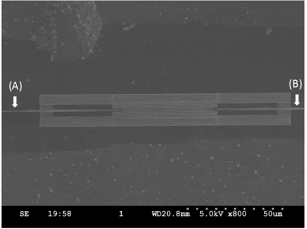
[image:21.612.156.457.260.484.2](A) (B)
Figure 2.1: Suspension of large, hundred-µm scale strutures
Large, hundred-µm scale structures can be suspended by sub-µm scale Nitride beams, millimeters away from attachment point to substrate. This figure depicts a
defect-mode photonic crystal waveguide device, embedded in a large mechanical support frame. The structure is suspended only by the waveguides (object A and B
in this figure), connecting eventually to the Silicon substrate (far left and right beyond the edges of this image).
Avoiding stress concentration
Silicon Nitride is a mechanically resilliant material with reported tensile yield
strength in the ∼ O(GPa) range[32], but its high intrinsic tensile stress (' 1GPa [33]) can cause various mechanical issues. Improper geometry design can create
device layer after being released from the Silicon substrate can be significantly
higher than the initial tensile stress. Sharp corners should be avoided, as they create
significant concentrated stress and can initiate a propagating crack. In case sharp
corner geometries are required due to desired optical properties, suitable support
structures such as tethers should be added to redistribute the mechanical stress, or
make the corner into a compressive corner. The other common situation to cause
stress concentration is when a thick section of Silicon Nitride is connected to a
thin one. Like a heavy spring connected to a thinner spring under load, the larger
structure will release its stress and shrink in size, redistributing all strain onto the
thin section and create high stress. This should also be avoided in design. See
Figures 2.2 through 2.3.
Stress balancing to prevent deformation
Fully releasing the initial∼1GPa tensile stress of the material produces a 0.5% strain change. This influence becomes amplified by the large aspect ratio of our devices to
create large deformation. The waveguides must terminate into free space to couple
to external optics, creating a zero-stress boundary that is free to move. For our
typical 2mm devices and without stress balancing, a∼ 5µm pull-in deformation is observed at the each of the waveguide terminations. Additionally, stress imbalance
could lead to significant deformation of the released structure as compared to the
lithographycally defined shapes on substrate. This can create a systematic error
for parameters such as the size of the vacuum gap in a double-beam structure; see
Figure 2.4.
We try to tackle this by arranging the device in a geometric configuration that
balances tension force at all junctions, with designs such as in Figure 2.5, whenever
possible. In case the deformation is inevitable, their influence must be taken into
consideration and compensation prior to lithography steps.
2.3 Thermal Conductance Structures
In order to provide thermal conduction for our structures, we make use of the
anchoring structure as described in [34]. The anchoring junction comprises a
widened waveguide supported by a set of thin periodic tethers. The tether array
with small (220nm) lattice constant behaves as an effective uniform but lower
index material, allowing the guided mode to be index-guided in the widened center
waveguide and preventing scattering into the tethers. With each device, we build two
(A) (B)
Figure 2.2: Geometries that create local heightened stress
This plot shows simulation of mechanical equilibrium stress distribution of released structures. The color plot is the resulting Von Mises stress of the material. (A) Connecting a larger (left half) piece of stressed material to a smaller one (right
half) results in the strain of the system to accumulate on the smaller one, hence resulting in heightened stress compared to the larger one. (B) Sharp corners, where the center horizontal beam connects to the left side of the plot, produces very large
local stress. Making a fillet of finite radius alleviates this issue, as shown in the right half of the plot.
Figure 2.3: Tensile versus compressive corners
This figure depicts a square hole with sharp corners embedded in a material stretched horizontally. The thin red arrows indicate deformation vector, and the color plot shows the Von Mises stress of the material. The up and down corners are
’tensile corners’ (red solid arrows), meaning they are being pulled apart and hence produce high stress concentration in their vicinity. The left and right corners are ’compressive corners’ (green solid arrows). We can observe the relatively lower stress associated with the compressive corners on this plot, compared to the tensile
(A)
(B)
Figure 2.4: Mechanical design to handle deformation
As an example for the deformation caused by stress, consider building a structure to split a single-beam waveguide into double-beam. (A) A naive design of direct tapering would deform under sufficient tensile force on the single beam, due to the
finite rigidity of the material. (B) Properly shaped splitter design creates significantly less deformation than the previous design under the same tensile force. The deformation is magnified by a factor of 5 on this plot for visibility. The
color plot indicates total displacement.
heat-sinks. The tether arrays conduct heat from the main waveguide onto the rails,
then further dissipate this heat into the Silicon substrate via the larger cross-section
area and hence thermal conductivity of the rails.
The efficiency of thermal dissipation can be characterized by the effective thermal
resistance ZT = AσLSi N, whereσSiN = 30W ·m/ ◦
C is the thermal conductance for
Silicon Nitride. For simplicity of estimation, we will assume the heat from the optical
mode is being deposited at the center of the device. A typical 2mm length suspended
device would have a thermal resistance of ZT =0.5· 200nm·5001mmnm·σSi N =170
◦C/µW
absorbed power, compared to the devices with heat sink tethers and rails where
ZT =0.25·(Ztet her s+Ztail)=0.25·(200nm·1575·100µmnm·σSi N+ 1
mmm
200nm·5µm·σSi N)= 10 ◦
C/µW. We note the factors of 0.5 and 0.25 are associated with that the device is two-sided
in its propagation direction, and each side has two rails. The factor of 15 inZtet her s
stands for the typical number of tethers used per array.
2.4 Connecting Waveguides to Outside World
We have explored two methods for coupling light into our devices. We initially
adapted the fiber-based adiabatic tapering technique in [34] to our wavelength and
Figure 2.5: Angled tether array for force balancing
The terminated tip of the coupling waveguide of a typical device. The main waveguide to the left of the image carries strong tensile stress. A set of tether array
anchors the tensile force of the waveguide into the substrate, preventing pull-in of the thin waveguide termination to prevent damage. The tether tilt angleθsatisfies 2ntet her ·wtet her sin(θ)=wwaveguide to cancel the total force on the junction on the
left.
profile at the end of the device has both small (NA=0.11) numerical aperture and
low (ne f f −1 = 0.003) effective mode index. The small divergence angle and the low residual reflection at the waveguide termination further allow us to develop a
direct coupling technique using asphereic lenses.
FEM calculation and mode projection
Various methods [34, 35, 36] have been developed to match the guided mode profile
of a photonic waveguide with sub-µm thickness to the mode of a conventional optical fiber, which is typically few µm in mode-field diameter. For our case, we taper the waveguide to make its guided mode highly evanescent in order to match
the larger fiber mode profile. A Finite-Element Method (FEM) calculation using COMSOL Multiphysicswas carried out to calculate the guided mode profile for given
waveguide width and optical frequency. We than select the waveguide geometry that
produces the highest mode overlap to the fiber mode. For our specific application,
we match the mode of a rectangular waveguide of 140nm by 200nm cross-section
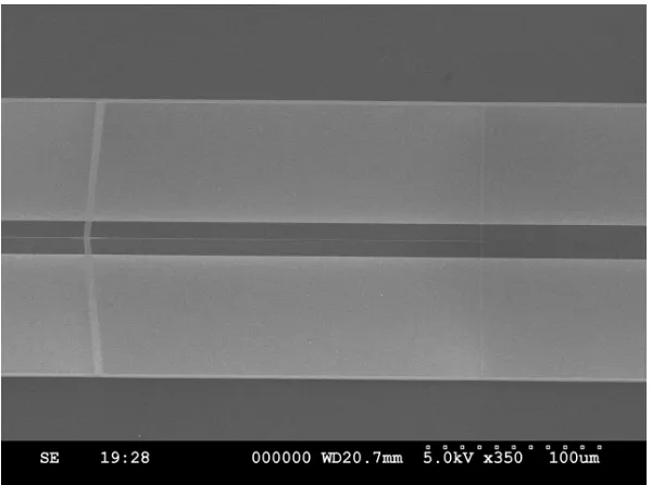
Figure 2.6: Waveguide and cooling rail
The suspended waveguide (lower horizontal structure) is connected to the cooling rail (upper horizontal structure) by a tether array.
The calculation result using a mode-projection calculation as described in [28] is
plotted in Figure 2.7. The two polarization modes of the waveguide generally have
different efficiency for a given waveguide width, unless we operate at 200nm-square
geometry.
Direct time-domain simulation
We make use of Finite-Difference Time-Domain (FDTD) methods to directly verify
the coupling efficiency at interfaces between various optical components on our
waveguide, and also between the waveguide and an external coupling channel.
FDTD computational time scales unfavorably with total simulation length in the
propagation direction, as the enlarged simulation volume compounds with the longer
run-time required for the injected excitation to propagate through the length of the
simulation volume. The simulation is typically done component-by-component as
opposed to the entire device, due to computational resource limitations.
Here we use the commercial FDTD packageLumerical FDTDto simulate launching
a wave packet of∼O(30THz) bandwidth from either a cleaved fiber-end or a Gaussian beam generated by the program into a highly-evanescent nanobeam waveguide.
The program then Fourier transforms the transmitted field at the other end of the
Figure 2.7: Coupling waveguide mode projection into Gaussian beam profile
The guided modes of the coupling waveguide for our devices are highly evanescent and can be matched to a Gaussian mode profile with reasonable efficiency [34]. The width of the waveguide determines the optimum beam waist for the Gaussian
beam.
project this power into the guided mode profile of interest using the method described
in previous subsection, 2.4. See Figure 2.8 for a simulated mode profile.
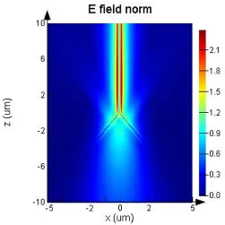
(A) (B)
Figure 2.8: FDTD simulation plot of free-standing coupling waveguide
(A) A Gaussian beam source is launched upward from the bottom of this plot, which then couples into the guided mode of the Silicon Nitride waveguide with optimally matched field profile. (B) Once the initial fiber mode is guided on the coupling waveguide, it is gradually transformed into a more localized waveguide
mode by an adiabatic taper.
2.5 Anti-Reflection Designs on Highly Evanescent Waveguides
To provide structural support and thermal dissipation channel for the waveguide,
structural components need to be designed to suppress residual reflection and loss.
This is particularly difficult at the coupling waveguide section, where the guided
mode becomes highly evanescent to match the fiber mode, as shown in Figure
2.8. The formerly used ’tether array on wide waveguide’ method as described in
section 2.3 can no longer be applied. A pair of 100nm tethers attached to the end
of the waveguide would produce approximately 1.0% reflection for the TE guided
mode; see Figure 2.9. In the coupling waveguide section, we are also restricted
by the minimum tether size of ∼80nm before fabrication yield becomes an issue. In this section, we develop anti-reflection designs specifically for this evanescent
[image:28.612.165.417.268.518.2]waveguide.
Figure 2.9: Reflection from coupling waveguide support tethers
This figure depicts the input of a Gaussian beam onto the coupling waveguide, similar to 2.8, but with a set of tethers for mechanically support. The tethers create
reflection, as visible in the interference fringes in the lower half of the plot. The reflection from the tether junction would then back-reflect into the input source and
interfere with the reflected signal from the device, creating difficulty in signal analysis.
’Round-about’ anti-reflection tether junction
One method we have experimented with to suppress reflection of the tether pair
and uniform waveguide does not create scattering. It is the polarization of the
additional material, namely the tethers, that creates a dipole moment and generates
the reflection and scattering at the junction. The intuition for this design is that
removing material from where the uniform waveguide would originally occupy
is effectively the same as adding material of negative polarizability to the total
scattering material, in hope to cancel the total scattering dipole moment. Therefore
we hope that by opening a hole in the path of the original unpatterned waveguide,
the dipole moment associated with the tethers can be partially cancel.
The geometry design is based on fillets on the tether-waveguide junction corners
to provide mechanical support, then opening a circular hole on the path of the
waveguide, see Figure 2.10. This has the advantage in mechanical consideration as
well, eliminating the sharp corners formed by the tether-waveguide junction with
fillet structure. We calculated using FDTD method that adding a 300nm radius
fillet reduces the transmission of the junction to 72%, but further opening a hole
of 270nm diameter restores it to 83%. Note that the numbers quoted here are from
the waveguide guided mode before and after passing the tether junction. With both
modifications, the reflection can be suppressed from 1.0% to 0.1%.
=
+
-‘Roundabout’ coupler-tether junction
Unperturbed waveguide (non-scattering)
Addition of material for tethering
[image:29.612.159.451.399.619.2]Removal of material due to hole
Figure 2.10: Concept of hole-based dipole cancelation tether
The removal of material from the originally unpatterend waveguide effectively creates a ’negative-polarizability’ material to partially cancel the total scattering
Y-shaped free-space coupling tether design
Devices designed for free-space coupling allow more available tethering geometries,
due to the the releasing of the half-plane of space that was occupied by the cleaved
fiber-end. We experimented with a design where the tethers are tilted from the
perpendicular direction to the waveguide by a sharp angle. This design makes
use of the property of sub-wavelength objects with sharp aspect ratio, that they
tend to have anisotropic polarizability that favors their long direction as opposed
to the thin direction. The suppression effect is two-fold. Firstly, the projection of
the waveguide electric field onto the long direction of the tether is reduced, hence
reducing the polarization of each tether. Secondly, the two non-parallel tethers
partially cancel the total polarization of the system in a vectorial addition manner;
see Figure 2.11.
With this concept in mind, numerical optimization using the FDTD program was
carried out. We eventually settled on a tilt angle of 60◦ from perpendicular. The
FDTD simulations suggest a Gaussian-beam-to-waveguide transmission of 87% for
a 5µm beam spot and our frequency range of interest (Cs D1 and D2, 335.1THz to 351.7THz). This method produces an overall simpler design and better efficiency,
at the cost of no longer being able to directly couple to the cleaved end of an optical
fiber. A summery of optical performance of these devices can be found in Table
2.1; also see Figure 2.12.
Type Transmission Reflection
TE TM TE TM
Gaussian to 140nm waveguide 90% 66% <0.1% <0.1%
with 100nm tether 79% 65% 2.7% 0.6%
with Y-shape tether 87% 56% <0.1% <0.1%
Guided mode through 100nm tether 86% 98% 1.2% 0.5%
300nm fillet 270nm hole 83% 97% 0.2% 0.1%
Table 2.1: Summery of optical performance of coupling waveguide tethering designs
2.6 Assembly of Fiber-Coupled Chip
In the fiber-based optics-to-chip coupling scheme, optical fibers are directly attached
to the photonics chip. The core of the optical fiber must then be precisely aligned
to the terminated coupling waveguide. The transverse alignment of the fiber core
to the fabricated waveguide is enforced by the physical contact of the fiber and
the V-shaped grooves etched into the chip substrate. The distance of the fiber end
E0
Ptotal
E0
Ptotal
(A) (B) (C)
PL PR PL PR
PL PR
[image:31.612.158.454.75.289.2]PL PR
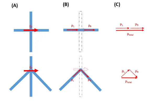
Figure 2.11: Dipole cancellation by tilted tethers
(A) We conceptually treat the tether junction as addition of dielectric as a perturbation being polarized by the guided mode electric field. (B) Due to the shape-dependent anisotropy of polarizability of deeply sub-wavelength objects, the
tethers primarily polarize along their long direction, with the angled tethers effectively only polarized by the parallel projection of the polarizing electric field.
(C) The total polarized dipole moment of the tethers is further reduced due to vectorial partial cancellation between the dipole moment of each tether.
real-time feedback of the optical signal from the fiber to be attached. Once aligned,
we affix the fiber to the chip using glue. The assembly process can take several
hours, and should be carried out in a properly clean environment to prevent chip
contamination.
Notes on using glue
We have experimented with the UV-cure glue as in [34] and also thermal-cured
glue for preferable higher-temperature performance and out-gassing properties; see
Table 2.2. A small droplet of glue is applied to the back end of the mounted fiber
using a suitable fine tool, in our case, a short length of stripped optical fiber. Upon
application, the glue seeps into the space between optical fiber and the Silicon groove
surfaces due to surface tension. It is critical that the glue must not be allowed to
overflow beyond the end of the cleaved fiber end. Should the coupling waveguide
become encapsulated by glue, it will no longer provide the correct mode profile, and
Figure 2.12: Angled tether design field plot
This is a FDTD field plot of an angled tether junction, where the optimal transmission tether angle from orthogonal was found to be π3. We see that the
interference fringe as seen in Figure 2.9 is strongly suppressed.
The UV-cure glue can be cured in sufficiently short time (flowing stops within <1s
exposure, full cure typically <1 minute) upon being irradiated by a UV lamp or UV
LED. The thermal-cure glue we used typically takes up to 10 minutes to fully cure
at elevated (∼ 100◦C) temperature, during which time the glue would flow until it reaches equilibrium. The total volume of glue drop determines whether the thermal
glue would overflow the device, and the slower cure time allows us to micro-adjust
the mounted fiber position during curing to eliminate any motion associated with
glue surface tension. Care must also be taken with the differential thermal expansion
between chip and holder, which could cause cracking due to thermal cycling. For
types and properties of the glues used in our project, see Table 2.2. A step-by-step
instruction for gluing can be found in Appendix D.
Fiber feedthrough and strain handling
We found that the adhesion strength between the glue and the Silicon substrate is
relatively low, compared to adhesion of the same glue to aluminum or Macor. This
the limited amount of glue we could safely apply without damaging the waveguide.
The low adhesion strength makes the fibers susceptible to tearing off the chip under
mechanical tension, particularly, if the tension force is perpendicular to the chip
surface. We did not notice difference in adhesion strength for the ALD coated
chips versus Nitride only chips. We partially alleviate the adhesion issue by putting
additional gluing point for the fiber further away from the chip and directly onto
the chip holder. At this position, more glue volume can be used without concern of
flooding the devices. The adhesion to the material of the chip holder (aluminum or
Macor) is also significantly stronger that to the Silicon chip.
We then run the fibers through the vacuum chamber by using Teflon feedthrough
as described in [37]. This feedthrough consists of a bulk piece of Teflon with
small through-holes drilled in to feed the fibers through. The feedthrough and
fibers are then compressed using aSwageloktube fitting, relying on the mechanical
compliance of Teflon, which is sufficiently soft to be able to conform to the fiber
jacket and the interior of the Swagelok piece, forming a vacuum seal. Multiple
fibers can be put through one feedthrough; we have experimented up to four fibers
per feedthrough. The highest number of devices we could connect this way for our
vacuum chamber is 8 devices with transmission and reflection channels (16 fibers
total). We try to minimize the residual length of fiber inside the vacuum chamber,
as their acrylate jacket remains a potential source of outgassing. Note that the
feedthroughs should be tested with a spare fiber prior to use, to confirm that the
holes are through. Forcing the device-coupled fiber could result in breakage. Also,
the tightening of the Swagelok to form the seal will cause it to attach tightly to the
fibers and is irreversible.
2.7 Coupling into Free-Space Lens-Coupled Chip
Migrating toward free-space direct coupling could provide several advantages for
our system, but also comes with its share of technical issues. Elimination of glue and
fiber would simplify the vacuum system, and allow for higher temperature baking.
Glue Curing Outgassing
Flow Stop Full Cure (Total Material Loss)
Torr-Seal 1hr, 90◦C 0.63%
Epo-Tek 353ND 5min at 120◦C 1hr, 150◦C 0.22% Dymax OP-67 <1s 1min, UV 3.33%
(A)
(B)
(C)
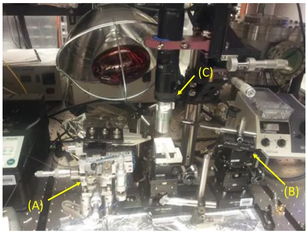
Figure 2.13: Fiber placement and automated glue application setup
An optical fiber is placed onto a five-axis stage actuated by high-precision differential screw micrometers (A), allowing fibers to be place safely into the V-shaped grooves etched into the chip substrate. A set of automated stages (B) can
then apply small droplets of glue in a controlled manner to attach the fibers. The process is monitored using a long working distance microscope (C).
Removal of mounted fibers on the chips can also reduce device footprint and increase
the number of usable devices per chip. Issues including optics working distance,
vibration, and lens and window aberration need to be taken into consideration in
designing a free-spaced based system.
Chip configuration adaption to allow free-space coupling
The typical coupling schemes to nanophotonic devices in a non-contact manner
are grating coupler [36] and butt-coupling [34, 35]. We opted for the later, due
to our device layer configuration. The mirror symmetry plane in the device layer
suggests that out-coming light from a grating coupler would emit equally upward
and downward from the device plane, imposing a maximum 50% one-way coupling
efficiency limit. Conveniently, since our devices are initially designed to match
the mode of conventional optical fiber, the alignment requirements and hence the
techniques to use are similar also to conventional fiber-coupling. The challenge for
the chip configuration would be to allow sufficient clearance for the free-space beam,
whose divergence is associated with the coupling waveguide numerical aperture. We
(A)
(B)
(C)
(D)
Figure 2.14: Chip holder assembly with fibers
This figure depicts the full chip-holder-fiber assembly ready for vacuum chamber. The chip is mounted on a Macor holder (A), then screwed onto an aluminum arm (B). Then, fibers are glued onto the selected devices, as shown in in this figure that a total of three devices are connected fully with transmission and refletion, and two
devices are connected only with one fiber, hence only allowing the reflection channel from one side. The fibers are reinforced by putting a second gluing spot directly onto the holder (C), and then attached directly to the aluminum arm (D) to
allow easy handling and installation into the vacuum chamber.
the waveguide at the edge of the chip. A guided precision cleaving technique was
developed to achieve this, as will be covered in the following chapter.
Vacuum and optics system consideration
The challenge on the vacuum system and optics side is then to provide the correct
beam spot and alignment from outside the vacuum chamber. It is also desirable
to have long working distance, to allow freedom of positioning the chip, and the
capability to manipulate the optical access by placing fixed mirrors in the vacuum
chamber. With the numerical aperture of our devices (NA=0.11), we found that a
working distance of up to 40mm can be achieved with commercial one-inch aspheric
lenses; see Table 2.3. Sending a non-coliminated beam through the window of a
vacuum chamber would lead to aberration of the beam, but correction optics for glass
thickness is well understood and commercially available. Thickness-compensated
the mode profile of the device mode can be directly imaged for the free-space
devices, and advanced free-space optics such as deformable mirrors or
Spatial-Light Modulators (SLM) can be applied to map the device mode into a desired
free-space or fiber mode with high efficiency.
(A)
(C)
(D)
(D)
(B)
Figure 2.15: Free-space direct-coupling test setup
The free-space coupling test setup comprises of (A) a five-axis stage with goniometer and rotation axis centered at the chip position (B). The translational stages are actuated with (C) both micrometer screws and piezoelectric stacks for fine adjustment. Then, two high-angular-precision mirror pairs (D) couple light
into the device’s either ends using the same technique as typically used in conventional fiber coupling. We found that once the the mirror pairs are aligned to the first device on the chip, the translation degrees of freedom on the five-axis stage are generally sufficient to translate from one device to the next while maintaining
sufficient coupling efficiency for successive devices.
Lens Diameter EFL WD NA
Device 0.11
Design target 25mm 40mm 35mm 0.34
Thorlabs A397-B 7.2mm 11mm 9.64mm 0.30 Thorlabs AL2550H-B 25mm 50mm 46mm 0.20
C h a p t e r 3
FABRICATION OF DEVICES
This chapter describes the fabrication process for our project. The process includes
electron-beam lithography to define the nanophotonics and their support structures,
plasma etching for pattern transfer, the etching of the substrate to release the devices,
and post-release processing. The majority of these techniques are standard in
semiconductor processing, so we were able to integrate them into our project with
varying degrees of adaption. With the fully developed process, we can typically
process 6 chips per fabrication cycle with 16 devices each, at a 90% yield rate.
For references on plasma etching, please see the thesis [39]. TheOxford Instruments
website also provides relevant information on their website page [40]. Information
regarding the critical point drying can be found in [41] or other thermodynamics
textbooks. The manufacturer’s website of our Atomic Layer Deposition (ALD)
machine provides some fundamental information on their website page [42]. A
step-by-step description of our fabrication recipe can be found in Appendix D.
Another useful resource would be the article [43], which includes comprehensive
tables of etch rates of various etchants and materials.
3.1 Fabrication Requirements
The fabrication of Silicon Nitride structures is reasonably well understood among
the semiconductor and nanophotonics communities. Some adaptions are made to
accommodate the properties of our devices, such as the aspect ratio and the device
footprint due to fiber and optical beam clearance. We tailor our fabrication process
to achieve the following targets:
• Precision in fabrication to allow alignment of device frequency responses to
atomic resonances
• Sufficient throughput and yield rate for millimeter-scale footprint devices
• Control of surface tension, bubbling, and cleanness during wet chemistry
Precision of device dimensions
The optical resonances of free-space Cesium atoms of interest for this project consist
of two invariant and spectrally narrow frequencies: the D1 (335.12THz) and D2
(351.73THz) manifolds. We then need to align the frequency responses of the
devices to that of the atom, while being constrained by finite fabrication precision.
This is achieved in two primary directions. Firstly, in the design phase, the device
geometry should be designed to have low sensitivity to dimension variation, so
that the same fabrication precision in dimensions corresponds to a finer sweep of
frequencies between devices. The geometry thus designed also reduces sensitivity
to imperfection and fluctuation. Secondly, the actual fabrication process should be
optimized for producing faithfully the dimensions that critically determines optical
properties, such as the photonic crystal parameters. Design paradigms that are
robust against small variation are preferred. For example, coupling between different
waveguide modes can be done using adiabatic tapering, but also phase-matching
methods. The former is efficient provided the taper is sufficiently long, and hence
robust against small variation in taper parameters, while the later require exact
matching between interfering channels.
Device footprint and throughput
The physical footprint of the functional section of our waveguides, typically the
photonic crystal section, are on the order of ∼ 100µm in length, and up to 30µm in width for the larger 2D-based devices. The few-mm length of our devices is
necessitated by spanning the through-window for compatibility with free-space
optics and laser cooling techniques, such as Magneto-Optical Trap (MOT)[44] or
Far-Off-Resonance Trap (FORT)[45]. For fiber-based devices, the width of each
device can be no smaller than the fiber diameter (125µm cladding without jacket). Having large footprint devices built to high precision resulted in long lithography
exposure time and limited the number of devices available per chip. The device
length also makes it susceptible to local errors, such as large point scatterers or
lithography machine stage stitching failure (see Figure 3.2). A single local error
anywhere on the waveguide length can completely ruin the waveguide device’s
performance, and in some cases cause mechanical breakage.
Issues associated with wet chemistry processes
Several properties of our chips make them particularly susceptible to damage during
(A)
(B)
(C)
(D)
Figure 3.1: Preliminary exploratory photonic crystals
(A) Early attempt to build double-beam photonic crystal using conventional hole-based design. In order to produce the small 15THz photonic band-gap (4.3%
gap-to-midgap ratio), very small holes are required, and become difficult to fabricate consistently. (B) Tapering the hole-based photonic crystals is ultimately
limited by the smallest hole size allowed by fabrication. Holes too small become only partially etched. (C) Inward-facing modulation in double-beam design. (D) Early corrugated photonic crystal design with outward-facing modulation. The sharp triangular shapes resulted from poor lithography exposure techniques prior
to the application of the ’grid’ method.
tension. Device designs with small (∼ O(200nm)) mechanical gaps could collapse from liquid surface tension. Also, the influence of some mechanical damage can
become amplified. An example to that would be broken support structures like the
side rails. A device with one of the two side rails broken would typically maintain
its optical properties, but liquid surface tension would cause it to tangle with the
waveguide and completely ruin the device. Having the devices pass through
liquid-air interface during the wet chemistry processes should be avoided. Secondly, in
order to etch the through-window, we simultaneously etch the Silicon substrate from
both sides. The chip should be placed in a configuration that avoids accumulation
of bubbles on both sides of the chip edges to avoid local masking. Accumulation
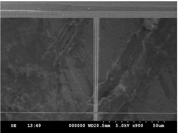
Figure 3.2: Stitching error
Stitching errors between main-fields are infrequent but can lead to reduced device yield. Transverse misalignment with small amplitude, as shown in this figure,
typically creates an unacceptable level of local scattering loss and residual reflection.
can occur on a microscopic scale (see [46]) and result in undesired features on the
etch surface, or in a macroscopic scale where large patches of the pattern become
covered and fail to etch. Finally, in order to allow the devices to tolerate the high
power density needed for atom trapping, aggressive cleaning procedures become
necessary.
3.2 Substrate Selection and Preparation
Our chips are fabricated from substrates of 200µm thickness Silicon. We ob-tain our substrates polished on both sides and coated with Si3N4 using the
Low-Pressure Chemical Vapor Deposition (LPCVD) process, which is carried out at
high (900◦C) temperature. This was preferred over the lower-temperature
Plasma-Enhanced Chemical Vapor Deposition (PECVD) process due to the reported (see
[47]) lower optical absorption for our wavelength range of interest. The 200µm sub-strate thickness was a compromise between the structural strength of the chip and
the feasibility of etching the through-window. We have experimented briefly with
the type of Silicon, such as P- or N-doped (50Ω-cm) or high-resisitivity (>5kΩ-cm),
which seem to produce no difference for our processes. We requested the
crystalline directions. The importance of precise alignment to the crystal axes will
be described in detail in section 3.4. We typically pre-clean the chips with solvent
chain and Piranha solution (see Section 3.6) before application of UV or electron
beam resists.
Pre-patterning the backside for through-window etch
We pattern a 2mm x 6mm rectangle on the backside of the chips, to allow the
through-window etching to progress from both sides. Since the optically critical
structures are typically suspended in the center of the through-window with large
clearance from the edges, the positioning of the back-window relative to the front
side patterns is non-critical, and a precision of few tens ofµm would suffice and can easily be achieved with UV lithography.
A UV lithography was carried out to define the back-window. We spin-coat the
UV resist Microchemicals GmbH AZ5214E on both sides of the chip at 4000rpm
and then carry out a 1.5 minutes bake at 100◦C to form a 1∼ 2µm film. The front side is first coated this way as a protection layer, and then the chips are flipped and
coated on the backside for UV exposure. The UV exposure is carried out using a
Chromium-on-glass mask, referencing the edges of the pre-diced chips. We use this
resist as a positive tone resist, and hence no post-bake is carried out, and the resist
is developed directly with Dow Microposit MF-CD-26 developer. The developed
rectangle pattern is transferred to the Nitride layer by plasma etching, then the
remaining resist can be removed using solvents (acetone, isopropyl alcohol, then
deionized water).
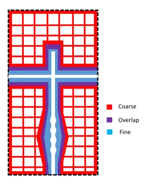
3.3 Electron Beam Lithography with Large Device Footprint
A pattern can be exposed in lithography using a positive tone resist (exposed area
is developed), or alternatively, have its inverse be exposed using a negative tone
resist (exposed area remains after developing). The pattern of our device contains
both large empty areas such as inside the grooves and window, and large filled areas
that are the remaining frame part of the substrate. For a single-exposure fabrication
process, large-area exposure will be unavoidable for either positive or negative tone
resists. An alternative method is devised to avoid large area exposure.
We expose our chip using aRaith EBPG 5000+lithography machine on theZeon Chemicals