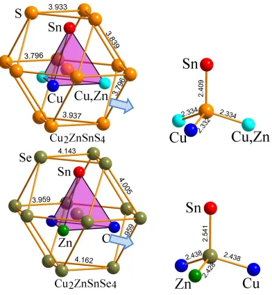
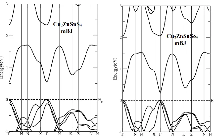
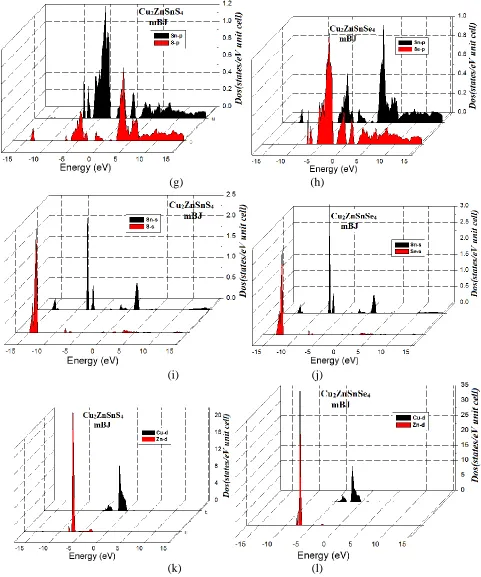
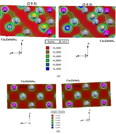
Structural, Electronic and Optical Properties in Earth-Abundant Photovoltaic Absorber of Cu2ZnSnS4 and Cu2ZnSnSe4 from DFT calculations
20
0
0
Full text
Figure
+2
Related documents