This is a repository copy of Suppression of Auger Recombination in Nanocrystals via Ligand-Assisted Wave Function Engineering in Reciprocal Space..
White Rose Research Online URL for this paper: http://eprints.whiterose.ac.uk/129852/
Version: Accepted Version
Article:
Califano, M orcid.org/0000-0003-3199-3896 (2018) Suppression of Auger Recombination in Nanocrystals via Ligand-Assisted Wave Function Engineering in Reciprocal Space. The Journal of Physical Chemistry Letters, 9 (8). pp. 2098-2104. ISSN 1948-7185
https://doi.org/10.1021/acs.jpclett.8b00248
© 2018 American Chemical Society. This document is the Accepted Manuscript version of a Published Work that appeared in final form in Journal of Physical Chemistry Letters, copyright © American Chemical Society after peer review and technical editing by the publisher. To access the final edited and published work see [insert ACS Articles on Request author-directed link to Published Work, see
https://doi.org/10.1021/acs.jpclett.8b00248.
[email protected] https://eprints.whiterose.ac.uk/ Reuse
Items deposited in White Rose Research Online are protected by copyright, with all rights reserved unless indicated otherwise. They may be downloaded and/or printed for private study, or other acts as permitted by national copyright laws. The publisher or other rights holders may allow further reproduction and re-use of the full text version. This is indicated by the licence information on the White Rose Research Online record for the item.
Takedown
If you consider content in White Rose Research Online to be in breach of UK law, please notify us by
Suppression of Auger recombination in nanocrystals
via ligand-assisted wave function engineering in
reciprocal space
Marco Califano
∗Pollard Institute, School of Electronic and Electrical Engineering, University of Leeds, Leeds LS2 9JT, United Kingdom
E-mail: [email protected]
Abstract
A limiting factor to the technological application of conventional semiconductor
nanostructures is their fast Auger recombination time. Strategies to increase it have so
far mostly focused on decreasing the electron-hole wave function overlapin real space
through structural modifications involving either elongation or shell growth.
Here we propose an alternative mechanism for Auger recombination suppression:
Graphical TOC Entry
Ligand 102 103 104 105Exciton storage time (ns)
A B C D E F
Electronegativity Low High
-0.1 -0.05 0 0.05 0.1
∆E (eV)
0.001 0.01 0.1 1 10 100 1000
Auger Recombination Time (ps)
Ligand A Ligand F
R = 1.1 nm
-0.04 -0.02 0 0.02 0.04
∆E (eV) 1 10 100 1000
Auger Recombination Time (ps)
Ligand A
Ligand F
R = 2.1nm
Zero dimensional semiconductor nanocrystal quantum dots (NQDs) are nearly-spherical
nanostructures which, owing to their 3D confinement, exhibit peculiar properties that set
them apart from those of the bulk material from which they are made. However, while
the size tunability of their optical properties and their inexpensive and relatively simple
colloidal synthesis make them ideally suited for a wide range of device applications in
very diverse fields,1–3 the exploitation of their full potential in such applications is
lim-ited by the presence of a non-radiative multi-exciton decay mechanism which has proven
especially efficient in these 0D systems, compared to the bulk and other low dimensional
systems: Auger recombination (AR). Indeed, in commonly synthesized colloidal
quan-tum dots, typical Auger recombination times range from a few to a few hundreds of
picoseconds,4 depending on the size. Such an efficient decay mechanism leads to large
non-radiative losses, limits optical-gain lifetimes and spectral bandwidths for optical
am-plification, and is therefore detrimental for applications ranging from biolabelling to
pho-tovoltaics and lasing. Attempts to slow down Auger recombination have focused so far
on the reduction of the overlap between electron and hole wave functions in real space,5
achieved by structural modifications such as elongation (quantum rods,6
quantum-dot-in-a-rod5) or shell growth (where a type II band alignment is formed at the
heterointer-face7,8). Core/giant-shell nanocrystals with a graded alloyed interface have also recently
been shown to greatly inhibit Auger recombination,9 an effect attributed to a
“smooth-ing” of the confining potential at the heterointerface.10 This procedure allows reductions
in the Auger recombination rates of two orders of magnitude or more, at the expense,
however, of a complex synthetic method (successive ion layer absorption and reaction
-SILAR) requiring long growth periods.9
The question we will address here is whether Auger recombination can be efficiently
suppressed without resorting to such time-consuming and costly procedures and, above
all, without modifying the morphology of the nanocrystal.
chemistry. Indeed, as a consequence of their chemical nature, NQDs are surrounded by a very complex environment, their surface being in contact with various chemical species
present in solution and different organic capping molecules, whose presence is needed to
ensure solubility, prevent aggregation and passivate surface dangling bonds.11,12Specific
capping groups are, however, also known to introduce localized states on the surface,
which can act as traps for either electrons or holes.13 Furthermore, the concentration14
and the quantity15 of surface ligands has been shown to be important, where deviations
from an optimal number lead to the formation of defect states in the gap.15
It was also recently shown experimentally16 that different capping agents could shift
the ionization energy of an ensemble of 4.7 nm diameter CdSe NQDs by up to 0.35 eV,
equivalent to the shift caused by a size (i.e. diameter) reduction of nearly 3 nm; other
groups17 have shown similar shifts (up to 0.3 eV) in the ionization potential and the local
vacuum level in tethered 3.6 and 6.0 nm diameter CdSe dots, depending on the
cap-ping group. Similarly, in InAs nanocrystals with 4.4 nm diameter, exchange of native
tri-octylphosphine (TOP) ligands with 4-methylthiophenol (MTP) and aniline, led to shifts
of the highest occupied molecular orbital (HOMO) by 0.2-0.3 eV and 0.3-0.4 eV
respec-tively.18 Other studies have found that surface ligands can affect the optical properties in
CdSe nanocrystals19,20(where the same ligand can have opposite effects, i.e., enhance the
PL or quench it, depending on the surface stoichiometry of the nanocrystal21), the rate
of electron intra-band relaxation in CdSe solutions,22 the intensity of surface emission in
CdSe dots,23 the optical band gap and the exciton confinement in CdS, CdSe, PbS24 and
CdTe nanocrystals,25 and even modify the stoichiometry26 or the overall morphology27
of lead chalcogenide nanocrystals. The specific surface chemistry of the NQD has also
been recently found responsible for other more subtle, but by no means less important,
effects, such as the control of the band-edge exciton linewidth.28 All these effects impact
the nanocrystal’s structure and/or its energetics. So far, however, apart from the creation
that the ligand’s presence could interfere with the core electron and hole wave functions
to such an extent as to result in a sufficient reduction in their overlap to suppress any
recombination mechanism to any degree.
An indication that this could be possible was provided by Reboredo and Zunger,29
who found theoretically that the exciton radiative lifetime in Ge NQDs could be modified
by changing the electronegativity of the nanocrystal’s passivating potentials. Although
in that case the main origin of the predicted long exciton lifetimes was a change in the
orbital symmetry of the VBM (which modified the allowed/forbidden character of the
lowest excitonic manifold), they also predicted a change in the Bloch-function
composi-tion in reciprocal space, from X to L, of the CBM wave funccomposi-tion. Similarly, Poddubny and
Dohnalová30 recently suggested the possibility of promoting direct-like band gap
transi-tions in Si NQDs (achieving over-2-orders-of-magnitude enhancements in the radiative
rates), by modifying their surface electronegativity.
These results hint to the tantalizing possibility of manipulating the wave functions in
reciprocal space through a simple ligand exchange procedure.
For such a manipulation to be effective, favourable conditions are: (i) a bulk band
structure featuring energetically closely spaced minima in the conduction band; (ii) large
differences between their effective masses; (iii) large values for the exciton Bohr radius.
There are a few materials that match these criteria (GaSb, GaAs, InP, and InSb). We
chose GaSb, which, although not presently synthesised colloidally, exhibits many
pecu-liar properties in the bulk that make it a promising candidate for device application at the
nanoscale. In particular, the separation between the conduction band minimum (CBM)
at Γ and the slightly higher minima at the L-points is only about 80 meV, whereas the
ratio of the effective masses at these high symmetry points is larger than 2.31 It is
there-fore expected that confinement should induce a Γ-to-L transition in the character of the
conduction band minimum, similarly to what was predicted to occur in GaAs,32 where,
and the exciton Bohr radius is nearly half of that in GaSb. The valence band of GaSb,
in-stead, has the structure common to all zinc-blende semiconductors, hence itsΓcharacter
is not expected to change with confinement. As a consequence, a confinement-induced
reduction of band edge electron and hole wave function overlapin reciprocal spaceis
ex-pected in this material, which could lead to a suppression of Auger recombination rates
in GaSb NQDs of suitable sizes. At the same time confinement should also induce a
direct-to-indirect band gap transition in these nanostructures which should result in long
exciton storage times.
The important question to ask, however, is whether the CBM composition (hence the
electron and hole wave function overlap) in reciprocal space can be modified via ligand
exchange for thesame nanocrystal size.
We consider nanocrystals with two different sizes,R=1.1 nm andR=2.1 nm, which
are built with bulk-like crystal structure, starting from a central anion, up to the
de-sired radius R. This procedure yields unsaturated bonds at the dot surface, which are
passivated here by 6 different sets (indicated by the capital letters A to F) of
pseudo-hydrogenic, short-range potentials with Gaussian form,
v(r) =αe−(|r−R(γ)|/σ)2 (1)
chosen to reproduce specific effects (see below) of realistic capping groups. Each model
ligand is characterized by (i) the amplitudeα and (ii) the widthσof the Gaussian
poten-tial, and by (iii) the distanceγdfrom the surface atom along the ideal bond line connecting
it with the missing atom (dis the bond length andR(γ)is the ligand position).33–35This is
clearly an oversimplified model for a complex organic molecule. Nevertheless, it is
suffi-ciently detailed to capture the essential properties of the capping agent’s most important
component: its binding moiety. Indeed, as it will be discussed later on in the paper, it has
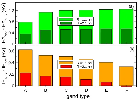
0 0.4 0.8 1.2 EA dot - EA bulk (eV)
R =1.1 nm R =2.1 nm
Ligand type 0 0.2 0.4 0.6 IE bulk - IE dot (eV)
R =1.1 nm R =2.1 nm
A B C D E F
(a)
[image:9.612.187.425.63.234.2](b)
Figure 1: Electron affinity and ionization energy dependence on surface ligand for GaSb
NQDs withR=1.1 nm andR=2.1 nm (both quantities are reported relative to the bulk
values).
responsible for the features we are interested in.
Both anion and cation surface atoms are passivated using the same procedure in order
to remove the corresponding trap states from the gap. However, we only vary the cation
passivation parameters α and γ in sets A to F (see Supporting Information), to model
different realistic ligands, as the capping groups usually bind to the metal atom on the
surface36 (Further details on the method can be found in the Supporting Information).
Nanocrystal’s ionization energy and electronegativity of the binding moiety
The effects of these 6 ligand typologies on the electron affinities (defined asEA=Evacuum−
Ecbm - green bars), and ionization energies (defined as IE=Evacuum−Evbm - red and
or-ange bars) of both GaSb nanocrystal sizes is shown in Figure 1. The ror-ange of
ligand-induced variations in the IEs calculated here (290 meV and 241 meV for R =1.1 nm
and R=2.1 nm, respectively) is comparable to that observed in CdSe (300 meV17 to 350
meV16), and InAs (400 meV),18suggesting that our model ligands reproduce realistically
the behaviour of a variety of real capping groups.
From Figure 1 it is also clear that ligands A to F have an increasingly confining
ef-fect on the electron, consistently with the parameters that characterise them (see Table S1,
Ligand type
0 20 40 60 80
Charge density within R/2 (%)
R = 1.1 nm R = 2.1 nm
A B C D E F
A C F
F C
[image:10.612.189.425.65.241.2]A
Figure 2: Main panel: Fraction of electron CBM charge density contained within a sphere
of radius R/2 from the dot centre for NQDs with R=1.1 nm (red squares and line) and
R=2.1 nm (blue squares and line). Top insets: 3D electron charge density in aR=2.1 nm
radius GaSb nanocrystal capped by ligands A, C and F. Bottom insets: 3D electron charge
density in aR=1.1 nm radius GaSb nanocrystal capped by ligands A, C and F. The blue
and cyan spheres represent Ga and Sb atoms, respectively.
higher levels (i.e., away from the bulk band edge), while, at the same time, decreasing
the valence band edge distance from the bulk value. These results therefore highlight the
close link between electron confinement and IE. Such an increased confining effect,
ob-tained without reducing the nanocrystal size, is precisely the feature required to achieve
the desired increase in theLcontent of the electron wave function.
The extent of the ligands’ influence on the carrier’s localisation is further characterised
in Figure 2, where we plot the fraction of the CBM electron charge density contained
within a sphere of radius R/2 from the dot centre. As the volume of such a sphere is
1/8 of the total dot volume, if the carriers were distributed uniformly throughout the
nanostructure, we would expect to find 12.5% of their density there. This seems to be the
case for a ligand-A capping in both dots, whereas the relative charge density increases
steadily for dots passivated with B to F (up to about 45% in the smaller dot, and to 54%
in the larger dot), consistently with the increased electron confinement deduced from the
calculated electron affinities (Figure 1). An inspection of the 3D CBM charge densities
and of the CBM density profiles calculated for passivants A and F (Figure S1,
Support-ing Information), however, reveals that, far from beSupport-ing uniformly distributed, the
elec-tron charge density relative to dots capped by ligand A exhibits a larger concentration
close to the surface, on atomic planes rich in Ga atoms with two dangling bonds. The
opposite is true for nanocrystals whose surface is terminated by passivant F, where the
largest concentration occurs at the dot centre. We therefore conclude that ligands from
F to A display an increasing efficiency to attract the electron, i.e., increasing
electroneg-ativity. This causal link between the ligand’s electronegativity and the resulting shift in
the nanocrystal’s IE is consistent with the available experimental evidence.16,18 Indeed,
Soreni-Harariet al.18 linked the shifts they observed in the HOMO energy of InAs NQDs
terminated by different ligands with the electronegativity of their binding moiety (with
the more electronegative anchor group inducing the largest IE). They concluded that the
most important role in determining the shift was played by the binding moiety itself, by
failing to observe any correlation between the capping molecule’s polar terminal group
and the shift induced. A similar conclusion was reached by Jasieniak et al.,16 regarding
the ionization energy in CdSe NQDs capped with different ligands, where variations in
surface moiety were found to induce changes from 0.05 eV up to 0.35 eV, whereas no
appreciable changes were induced by variations of the alkyl chain length for each of the
moieties. This evidence also directly confirms the suitability of our simplified ligand
model for the purposes here investigated. Based on these results and on the analysis
pro-posed for InAs NQDs,18 given the similarity in magnitude of the shifts we calculate to
the experimentally observed ones, we therefore expect: (i) our A-F ligands to modelreal
ligands featuring different binding groups; (ii) the ligand producing the largest shift (A,
see Figure 1) to replicate the characteristics of the passivant with the most electronegative
anchor group in the set; and (iii) ligands producing increasingly smaller shifts to model
real ones having moieties with decreasing values of electronegativity.
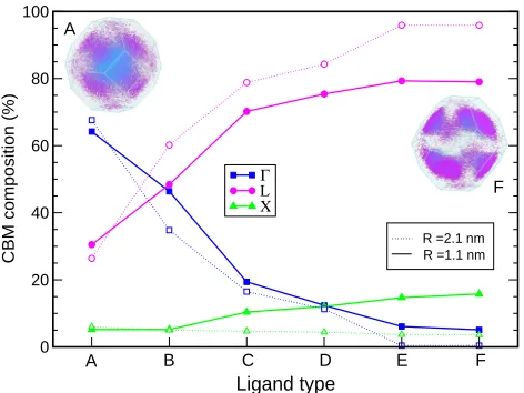
Ligand type
0 20 40 60 80 100
CBM composition (%)
Γ
L X
A B C D E F
R =2.1 nm R =1.1 nm
[image:12.612.189.425.64.241.2]F A
Figure 3: k-vector decomposition of the CBM wave functions for R=1.1 nm (solid lines
and full symbols) and R = 2.1 nm (dotted lines and empty symbols) NQDs: Γ, blue
squares; L, magenta circles; and X, green triangles (the lines are a guide to the eye). The
insets display the 3D Brillouin zone calculated for aR=2.1 nm NQD capped by ligands
A and F, where the k points are color coded according to the main panel: blue, close toΓ
and magenta, close to L.
as we repeatedly stressed, our approach only allows us to model the properties of the
ligand’s binding group. Therefore, proceeding further to assign a specific molecule to
each of our model ligands would involve a large degree of uncertainty and
arbitrari-ness. This task is complicated even further by the lack of consensus in the literature on
the viable passivations for Ga-based nanocrystals: while Alivisatos’ and Weller’s groups
used trioctylphosphine (TOP)52 and trioctylphosphine oxide (TOPO)53as surfactants for
their GaAs and GaP nanocrystals, recent attempts by Talapin’s group to stabilize GaAs
nanocrystals with traditional organic ligands (including, apart from TOP and TOPO, also
various combinations of oleylamine or hexadecylamine, oleic acid, dodecanethiol, and
octadecylphosphonic acids) proved unsuccessful.54 Therefore, having shown that our
model ligands are realistic, we are however unable to identify them with specific
cap-ping molecules.
Analysis of the electron wave function in reciprocal and real space
composi-tion of the nanocrystal’s core states is expected to be linked to the IE shifts they induce,
since to small values of the IE correspond increased confinement andvice versa, and
con-finement is expected to affect the character of the CBM in reciprocal space. The results of
a k-vector decomposition of the conduction band edge wave function in terms of
high-symmetry point components, presented in Figure 3, show a strong ligand dependence of
theΓand L contributions to the CB wave functions. The confinement-inducedΓ-to-L
tran-sition of the GaSb CBM, expected to take place in much larger dots,37is strongly inhibited
by ligand A and only slightly allowed by ligand B (for whichΓand L contributions have
almost equal magnitude), in the smaller dot. Nanocrystals capped with ligands C-F show
instead CBMs with majority L character, which increases from C to F (as does their
con-fining effect), and, accordingly, decreasing contributions fromΓ. A very similar behavior
is exhibited by the larger dot, where it is also accompanied by a change in the CBM
en-velope function symmetry, from prevalently s-like, for dots capped with ligands A - D,
to p-like, for dots terminated by ligands E and F. The VBM envelope is found instead to
bes-like only for ligand A, whereas its symmetry is p-like for all other ligands (further
details on the symmetry of the band edges can be found in the Supporting Information).
Exciton and multi-exciton recombination rates
The Γ-to-L transition in the CBM character should lead to a reduction in the CBM-VBM
wave function overlap (and to a direct-to-indirect band gap transition) in reciprocal space,
since the VBM remains mainlyΓ, irrespective of surface termination. As a consequence,
the Auger recombination time and the exciton radiative lifetime are expected to increase
from dots capped with ligand A (exhibiting aΓ-like CBM), to F, where the L character is
most pronounced.
Our results, presented in Figure 4, Figure 5 (black squares and line) and Figure S2
(Supporting Information), confirm these expectations, showing an astonishing
over-two-orders-of-magnitude suppression of Auger recombination (i.e., comparable to that achieved,
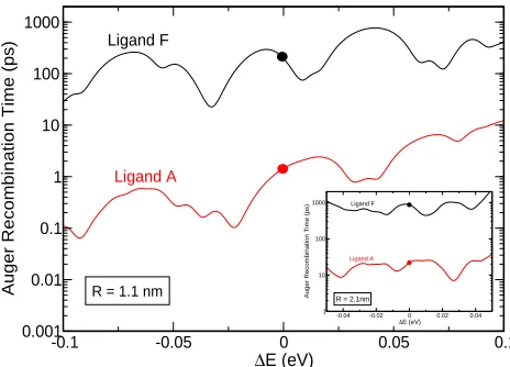
-0.1 -0.05 0 0.05 0.1
∆E (eV)
0.001 0.01 0.1 1 10 100 1000
Auger Recombination Time (ps)
Ligand A
Ligand F
R = 1.1 nm
-0.04 -0.02 0 0.02 0.04
∆E (eV) 1
10 100 1000
Auger Recombination Time (ps)
Ligand A
Ligand F
[image:14.612.189.421.64.231.2]R = 2.1nm
Figure 4: Auger recombination times in toluene calculated for GaSb NCDs with R=1.1
nm, capped with ligands A (red line) and F (black line), as a function of the variation in the
band gap energy around the value (∆E=0) predicted for that specific size. ∆Eaccounts
for ensemble structural effects (size distribution or shape anisotropy) and the influence of the nanocrystal environment (local electric fields and/or charge fluctuations). The inset
displays the results for R=2.1 nm. For illustrative purposes, the range of variation for
∆E shown (100 meV and 50 meV forR=1.1 nm and R=2.1 nm, respectively) is larger
than realistically expected.
and a nearly-three-orders-of-magnitude increase in lifetime from A- to F-capped dots for
both sizes considered. In Figure 4, where the AR time is shown as a function of the
varia-tion∆Ein the band gap energy around the value (∆E=0) predicted for the specific sizes
considered,39 the AR time calculated at ∆E=0 for a R=1.1 nm dot ranges from 1.5 ps,
for capping with ligand A, to about 200 ps, for ligand F termination. Its largest variation
(occurring within less than one LO phonon energy from∆E=0) spans however 3 orders
of magnitude, from 0.1 ps to 100 ps, whereas the longest calculated AR time approaches
the ns range in F-terminated NQDs. Similarly, in a dot with R=2.1 nm, the AR time at
∆E=0 ranges from 22 ps (ligand A) to 866 ps (ligand F); whereas the largest variation
(still within ¯hωLO from ∆E =0) is from 7 ps to 1013 ps, reaching into the ns range for
F-capped nanocrystals. In comparison, InAs and InSb NQDs withR=2.1 nm exhibit AR
times of a few ps.40–43
From simple bulk scaling arguments4it can be shown that the tri- and quadri-exciton
pre-dicted from the calculated bi-exciton AR times τ2. Our results show that 4-exciton AR
times in GaSb nanocrystals withR=2.1 nm can be engineered to exceed 200 ps, by using
appropriate capping agents. In contrast,τ4values measured in CdSe dots of similar sizes
are of the order of a few ps, i.e., about two orders of magnitude faster.4
It should be noted that, since a specific passivant modifies both AR and PL times in
the same direction (i.e., F increases both, A decreases both), F-terminated nanocrystals
will be ideally suited for applications requiring long carrier lifetimes, such as PV or
bio-labelling (a new time-gated immunofluorescence imaging method49 was recently made
possible by NQDs with photoluminescence lifetimes in theµs range). On the other hand,
as in such nanocrystals the radiative lifetime increases more than AR lifetime, they will
exhibit a lower biexciton quantum yield50 (reduced by a factor of 2 in the smaller
struc-tures and nearly by one order of magnitude in GaSb nanocrystals with R=2.1 nm) than
A-capped dots, which will be therefore better suited for applications such as LEDs, single
photon sources and lasers. In this respect, it is however interesting to note that even
core/giant-shell nanocrystals exhibiting complete blinking suppression9 can exhibit51
biexciton quantum yields≪0.1, and, hence, a much reduced degree of AR suppression.
Excitonic structure and Stokes shifts
A further origin for the lifetimes increase we predict is the symmetry change of both
VBM and CBM (whose implications on the optically allowed or forbidden character of
the excitonic states derived from them are discussed in the Supporting Information). In
nanocrystals capped by ligand A we find that the ground state exciton is dark. However,
the bright exciton is only 0.15 meV higher in energy (i.e., thermally populated forT>1.7
K), leading to a short radiative lifetime. As a stronger transition with a larger oscillator
strength is located higher in energy, we find a significant global Stokes shift (70 meV)44
in this case. For surface terminations types B to D, the ground state exciton has instead
a dipole-allowed component, yielding a partially allowed ground exciton, with a much
Ligand type 101 102 103 104 105 106
Radiative lifetime (ns)
100 150 200 250 300
Stokes shift (meV)
A B C D E F
R = 2.1 nm
1 1.2 1.4 1.6 1.8
Energy (eV)
Normalised Intensity
1 1.2 1.4 1.6 1.8
Energy (eV)
[image:16.612.189.423.65.214.2]Normalised Intensity
Figure 5: Room temperature radiative recombination times (black squares and line - left y axis), in toluene, and Stokes shifts (red circles and line - right y axis) calculated for
NCDs with R=2.1 nm, capped with different ligands A-F (The lines are a guide to the
eye). The insets display the calculated normalised emission (black line) and absorption (red line) spectra (assuming a Gaussian broadening of 80 meV) for ligand A (top left) and F (bottom right). The red solid lines show the calculated absorption superimposed on a background increasing as the third power of the energy, whereas the red dashed lines show the Gaussian curve alone.
A. The Stokes shift calculated for dots capped by these ligands follows the trend of the
lifetimes, as a result of the progressive shift to higher energies of the fully allowed optical
transitions. Finally, for large dots capped by ligands E and F, the symmetry of the band
edges leads to a manifold of over 100 dark exciton states, (including degeneracies),
start-ing from the ground state upwards, yieldstart-ing (a) the longest lifetime calculated for this
dot size, nearly 3 orders of magnitude larger than for A-capped dots, and (b) the larger
Stokes shift, above 250 meV, for F-capped dots (see Figure 5 red circles).
Large separations between emission and band edge absorption (referred to as “global
Stokes shifts”) suppress photoluminescence self-absorption and are therefore beneficial to
all applications exploiting light emitted from the dot (LEDs, biological imaging,49lasers,
solar energy harvesting,45,46 etc.). Although the Stokes shifts obtained here are smaller
than those achievable using core/giant-shell nanocrystals,45or dopants,47their tunability
through the choice of the surface termination presents a simpler synthetic alternative.
To the best of our knowledge there are no available systematic experimental studies on the
effect of different capping groups on AR rates. There are however studies on the effect of
ligands on intraband electron relaxation, which in colloidal nanocrystals can be due (and
is generally attributed48) to an Auger process. It is reasonable to assume that the reduced
overlap in reciprocal space responsible for the AR suppression discussed here, will
ap-ply to Auger electron cooling (AC) as well, given that the evaluation of the rate of the
latter involves the calculation of matrix elements containing both electron and hole band
edge wave functions. Therefore our AR suppression strategy could be indirectly
veri-fied using electron intraband relaxation data. A progressive increase in the electron
de-cay times measured in CdSe nanocrystals capped by tetradecylphosphonic acid (TDPA),
TOPO, oleic acid (OA), oleylamine (OLA), and n-dodecanethiol (DDT), respectively, was
indeed reported by Guyot-Sionnest et al.22 Considering that the electronegativity of the
binding moiety of these ligands decreases from TDPA to DDT, these observations are
consistent with our model. Furthermore, they suggest (a) that the applicability of our
strategy extends to most materials, irrespective of whether their bulk band structure
ex-hibits closely-spaced minima in the conduction band (condition (i) above) or not, but also
(b) that the extent of the Auger rates suppression does indeed depend on the band
struc-ture (in the case of CdSe, where there are no closely spaced minima, the observed increase
in the decay times was found22 to be at most a factor of 7, from 3.8 ps to 27 ps, for 4.5 nm
NQDs, compared to the orders of magnitude increase we predict in GaSb). Similar
con-siderations should also apply to the material’s optical properties, as was recently reported
for Si NQDs.55
It has to be mentioned that Guyot-Sionnest and co-workers interpreted their results
in terms of “energy transfer to electronic states mediated by the interfacial polarity or
energy transfer to high-frequency vibrations of the ligands."22 We note, however, that, as
in these experiments it was not possible to isolate the binding moiety (whose
was responsible for the high-frequency vibrations), and the surrounding environment, it
is difficult to determine to what extent each of these factors contributed to the observed
increase in the decay times. The picture is further complicated by the fact that surface
in-teractions in real samples are still poorly understood, despite the large number of studies
(both experimental and theoretical) on this subject. In our study we isolated the binding
moiety from the rest of the molecule, supported by experimental evidence that (i) this is
the main factor that determines the shift in ionization energy and (ii) this shift is linked to
the moiety’s electronegativity. We then proceeded to show that our model ligands could
reproduce the magnitude of the shifts produced by different real ligands in different
ma-terials, hence they were realistic models for the binding moieties of such ligands. Finally
we linked the moiety’s electronegativity with the k-space character of the electron wave
function and this to the AR rates.
In conclusion, we have presented a new, very simple and effective strategy to tune
radiative and non-radiative decay rates within an orders-of-magnitude-wide range, by
modifying the reciprocal space composition of the band edge states wave functions through
surface chemistry manipulation. Indeed, we found that by varying the electronegativity
of a ligand’s binding moiety it is possible to reproduce the effects of confinement - where
less electronegative anchor groups induce increased confinement andvice versa- hence to
induce variations in the symmetry and the k-space character of a core state, in materials
where the separation between two or more high-symmetry points in the bulk band
struc-ture is small. As a consequence, (i) Auger recombination can be suppressed to a degree
comparable to that achieved in core/giant-shell nanocrystals; (ii) the radiative lifetime in
the nanocrystal may be tailored to vary within nearly three orders of magnitude, while
(iii) the Stokes shift can be engineered to suppress PL self-absorption, by simple ligand
exchange procedures. This will enable a fuller exploitation of these nanostructures in a
Supporting Information Available
The parameters relative to the different model ligands A-F (Table SI); Method; Charge
Density profiles calculated for a NQD with R =2.1 nm capped with ligands A and F
(Figure S1); Symmetry of the band edge wave functions and character of the ground state
excitonic transitions; Radiative lifetimes calculated for a NQD with R=1.1 nm capped
with ligands A and F (Figure S2).
References
(1) Talapin, D. V.; Lee, J.-S.; Kovalenko, M. V.; Shevchenko, E. V. Prospects of Colloidal
Nanocrystals for Electronic and Optoelectronic Applications Chem. Rev. 2010, 110,
389-458
(2) Kovalenko, M. V.et al.Prospects of Nanoscience with NanocrystalsACS Nano2015,
9, 1012-1057.
(3) Kagan, C. R.; Lifshitz, E.; Sargent, E. H.; Talapin, D. V. Building Devices from
Col-loidal Quantum Dots.Science2016,353, aac5523.
(4) Klimov, V. I.; Mikhailovsky, A. A.; McBranch, D. W.; Leatherdale, C. A.; Bawendi,
M. G. Quantization of Multiparticle Auger Rates in Semiconductor Quantum Dots.
Science2000,287, 1011-1013.
(5) Zavelani-Rossi, M.; Lupo, M. G.; Tassone, F.; Manna, L.; Lanzani, G. Suppression of
biexciton Auger recombination in CdSe/CdS dot/rods: role of the electronic
struc-ture in the carrier dynamics.Nano Lett.2010,10, 3142-3150.
(6) Htoon, H.; Hollingsworth, J. A.; Dickerson, R.; Klimov, V. I. Effect of zero- to
one-dimensional transformation on multiparticle Auger recombination in semiconductor
(7) Oron, D.; Kazes, M.; Banin, U. Multiexcitons in type-II colloidal semiconductor
quantum dots.Phys. Rev. B2007,75035330.
(8) Osovsky, R.; Cheskis, D.; Kloper, V.; Sashchiuk, A.; Kroner, M.; Lifshitz, E.
Continuous-Wave Pumping of Multiexciton Bands in the Photoluminescence
Spec-trum of a Single CdTe-CdSe Core-Shell Colloidal Quantum Dot.Phys. Rev. Lett.2009,
102, 197401/1-197401/4.
(9) Chen, Y.; Vela, J.; Htoon, H.; Casson, J. L.; Werder, D. J.; Bussian, D. A.; Klimov, V.
I.; Hollingsworth, J. A. “Giant” Multishell CdSe Nanocrystal Quantum Dots with
Suppressed Blinking.J. Am. Chem. Soc.2008,130, 5026-5027.
(10) Cragg, G. E.; Efros, A. L. Suppression of Auger Processes in Confined Structures.
Nano Lett.2010,10, 313-317.
(11) Boles, M. A.; Ling, D.; Hyeon, T.; Talapin, D. V. The Surface Science of Nanocrystals
Nat. Mater.2016,15, 141-153.
(12) Green, M. The Nature of Quantum Dot Capping Ligands J. Mater. Chem. 2010, 20,
5797-5809.
(13) Houtepen, A. J.; Hens, Z.; Owen, J. S.; Infante, I. On the Origin of Surface Traps in
Colloidal II-VI Semiconductor Nanocrystals.Chem. Mater.2017,29, 752-761.
(14) Munro, A. M.; Plante, I. J. L.; Ng, M. S.; and Ginger, D. S. Quantitative Study of the
Effects of Surface Ligand Concentration on CdSe Nanocrystal PhotoluminescenceJ.
Phys. Chem. C2007,111, 6220-6227
(15) Kim, D.; Kim, d.-H.; Lee, J.-H.; Grossman, J. C. Impact of Stoichiometry on the
Elec-tronic Structure of PbS Quantum Dots.Phys. Rev. Lett.2013,110, 196802.
(16) Jasieniak, J.; Califano, M.; Watkins, S. E. Size-Dependent Valence and Conduction
(17) Munro, A. M.; Zacher, B.; Graham, A.; Armstrong, N. R.Photoemission Spectroscopy
of Tethered CdSe Nanocrystals: Shifts in Ionization Potential and Local Vacuum
Level As a Function of Nanocrystal Capping LigandACS Appl. Mater. Interfaces2010,
2, 863-869.
(18) Soreni-Harari, M.; Yaacobi-Gross, N.; Steiner, D.; Aharoni, A.; Banin, U.; Millo, O.;
Tessler, N. Tuning Energetic Levels in Nanocrystal Quantum Dots through Surface
Manipulations.Nano Lett.2008,8, 678-684.
(19) Talapin, D. V.; Rogach, A. L.; Kornowski, A.; Haase, M.; and Weller, H. Highly
Luminescent Monodisperse CdSe and CdSe/ZnS Nanocrystals Synthesized in
a Hexadecylamine-Trioctylphosphine Oxide-Trioctylphosphine Mixture Nano Lett.
2001,1, 207-211.
(20) Kalyuzhny, G. and Murray, R. W. Ligand Effects on Optical Properties of CdSe
Nanocrystals.J. Phys. Chem. B2005,109, 7012-7021.
(21) Jasieniak, J.; Mulvaney, P. From Cd-Rich to Se-Rich - the Manipulation of CdSe
Nanocrystal Surface Stoichiometry.J. Am. Chem. Soc.2007,129, 2841-2848.
(22) Guyot-Sionnest, P.; Wehrenberg, B.; Yu, D. Intraband Relaxation in CdSe
Nanocrys-tals and the Strong Influence of Surface Ligands.J. Chem. Phys.2005,123, 074709.
(23) Krause, M. M.; Jethi, L.; Mack, T. G.; and Kambhampati, P. Ligand Surface Chemistry
Dictates Light Emission from Nanocrystals.J. Phys. Chem. Lett.,2015,6, 4292-4296.
(24) Frederick, M. T.; Amin, V. A.; Cass, L. C.; Weiss, E. A. A Molecule to Detect and
Perturb the Confinement of Charge Carriers in Quantum Dots Nano Lett. 2011, 11,
5455-5460.
Nanocrystals through Chemical Surface Modification J. Am. Chem. Soc. 2005, 127, 1634-1635.
(26) Hughes, B. K.; Ruddy, D. A.; Blackburn, J. L.; Smith, D. K.; Bergren, M. R.; Nozik, A.
J.; Johnson, J. C.; Beard, M. C. Control of PbSe Quantum Dot Surface Chemistry and
Photophysics Using an Alkylselenide Ligand.ACS Nano2012,6, 5498-5506.
(27) Fang, C.; van Huis, M. A.; Vanmaekelbergh, D.; Zandbergen, H. W. Energetics of
Polar and Nonpolar Facets of PbSe Nanocrystals from Theory and ExperimentACS
Nano2010,4, 211-218.
(28) Gellen, T. A.; Lem, J.; Turner, D. B. Probing Homogeneous Line Broadening in CdSe
Nanocrystals Using Multidimensional Electronic Spectroscopy.Nano Lett. 2017, 17,
2809-2815.
(29) Reboredo, F. A.; Zunger, A. Surface-Passivation-Induced Optical Changes in Ge
Quantum Dots.Phys. Rev. B2001,63, 235314-1–235314-7.
(30) Poddubny, A. N.; Dohnalová, K. Direct band gap silicon quantum dots achieved via
electronegative cappingPhys. Rev. B2014,90, 245439-1– 245439-7.
(31) Miura, N. Physics of Semiconductors in High Magnetic FieldsOxford science
publica-tions, OUP Oxford, 2008, ISBN: 0198517564, 9780198517566
(32) Luo, J.-W.; Franceschetti, A.; Zunger, A. Quantum-Size-Induced Electronic
Transi-tions in Quantum Dots: Indirect Band-Gap GaAs.Phys. Rev. B2008,78, 035306.
(33) Wang, L.-W.; Zunger, A. Pseudopotential calculations of nanoscale CdSe quantum
dots.Phys. Rev. B1996,53, 9579.
(34) Fu, H.; Zunger, A. Local-density-derived semiempirical nonlocal pseudopotentials
(35) Graf, P.A.; Kim, K.; Jones, W.B.; Wang, L.W. Surface Passivation Optimization Using
DIRECT.J. Comp. Phys.2007,224, 824-835.
(36) Anderson, N. C.; Hendricks, M. P.; Choi, J. J.; Owen, J. S. Ligand Exchange and
the Stoichiometry of Metal Chalcogenide Nanocrystals: Spectroscopic Observation
of Facile Metal-Carboxylate Displacement and BindingJ. Am. Chem. Soc.2013, 135,
18536-18548.
(37) Califano, M. Characterisation of GaSb at the Nanoscale (unpublished).
(38) García-Santamaría, F.; Chen, Y.; Vela, J.; Schaller, R. D.; Hollingsworth, J. a; Klimov,
V. I. Suppressed Auger Recombination in ”Giant” Nanocrystals Boosts Optical Gain
PerformanceNano Lett.2009,9, 3482-3488.
(39) ∆Eaccounts for ensemble structural effects size distribution or shape anisotropy
-and the influence of the nanocrystal environment - local electric fields -and/or charge
fluctuations.
(40) Califano, M. Direct and Inverse Auger Processes in InAs Nanocrystals: Can the
De-cay Signature of a Trion Be Mistaken for Carrier Multiplication? ACS Nano2009, 3,
2706-2714.
(41) Schaller, R. D.; Pietryga, J. M.; Klimov, V. I. Carrier Multiplication in InAs
Nanocrys-tal Quantum Dots with an Onset Defined by the Energy Conservation Limit Nano
Lett.2007,7, 3469-3476.
(42) Sills, A.; Harrison, P.; Califano, M. Exciton Dynamics in InSb Colloidal Quantum
Dots.J. Phys. Chem. Lett.20157, 31-35
(43) Chang, A. Y.; Liu, W.; Talapin, D. V.; Schaller, R. D. Carrier Dynamics in Highly
Quantum-Confined, Colloidal Indium Antimonide NanocrystalsACS Nano2014, 8,
(44) Calculated assuming a Gaussian broadening of 80 meV for the optical spectra.
(45) Meinardi, F.; Colombo, A.; Velizhanin, K. A.; Simonutti, R.; Lorenzon, M.; Beverina,
L.; Viswanatha, R.; Klimov, V. I.; Brovelli, S. Large-area luminescent solar
concentra-tors based on ’Stokes-shift-engineered’ nanocrystals in a mass-polymerized PMMA
matrix.Nat. Phot.2014,8, 392-399.
(46) Meinardi, F.; Ehrenberg, S.; Dhamo, L.; carulli, F.; Mauri, M.; Bruni, F.; Simonutti, R.;
Kortshagen, U.; Brovelli, S. Highly efficient luminescent solar concentrators based on
earth-abundant indirect-bandgap silicon quantum dots.Nat. Phot.2017,11, 177-185.
(47) Buonsanti, R.; Milliron, D. J. Chemistry of Doped Colloidal Nanocrystals Chem.
Mater.2013,25, 1305-1317.
(48) Klimov, V. I. Optical Nonlinearities and Ultrafast Carrier Dynamics in
Semiconduc-tor Nanocrystals.J. Phys. Chem. B2000,104, 6112
(49) Tu, C.-C.; Awasthi, K.; Chen, K.-P.; Lin, C.-H.; Hamada, M.; Ohta, N.; Li, Y.K.
Time-Gated Imaging on Live Cancer Cells Using Silicon Quantum Dot Nanoparticles with
Long-Lived Fluorescence.ACS Photonics,2017,4, 1306-1315.
(50) We assume the radiative lifetime of the biexciton to be 4 times that of the single
exciton and the only (or the most efficient) nonradiative pathway to be AR.51
(51) Park, Y.-S.; Malko, A. V.; Vela, J.; Chen, Y.; Ghosh, Y.; Garcia-Santamaria, F.;
Hollingsworth, J. A.; Klimov, V. I.; Htoon, H., Near-unity quantum yields of
biex-citon emission from CdSe/CdS nanocrystals measured using single-particle
spec-troscopy.Phys. Rev. Lett.2011,106, 187401/1-187401/4.
(52) Beberwyck, B. J.; Alivisatos, A. P. Ion Exchange Synthesis of IIIâ ˘A¸SV NanocrystalsJ.
(53) Lauth, J.; Strupeit, T.; Kornowski, A.; Weller, H. A Transmetalation Route for
Col-loidal GaAs Nanocrystals and Additional IIIâ ˘A¸SV Semiconductor Materials Chem.
Mater.2013,25, 1377-1383.
(54) Srivastava, V.; Liu, W. Y.; Janke, E. M.; Kamysbayev, V.; Filatov, A. S.; Sun, C. J.;
Lee, B.; Rajh, T.; Schaller, R. D.; Talapin, D. V. Understanding and curing structural
defects in colloidal GaAs nanocrystals.Nano Lett.2017,17, 2094-2101.
(55) Lee, B. G.; Luo, J.-W.; Neale, N. R.; Beard, M. C.; Hiller, D.; Zacharias, M.; Stradins,
P.; Zunger, A. Quasi-Direct Optical Transitions in Silicon Nanocrystals with Intensity
Exceeding the Bulk.Nano Lett.2016,16, 1583-1589.