THESES SIS/LIBRARY TELEPHONE: +61 2 6125 4631
R.G. MENZIES LIBRARY BUILDING NO:2 FACSIMILE: +61 2 6125 4063
THE AUSTRALIAN NATIONAL UNIVERSITY EMAIL: library.theses@anu.edu.au CANBERRA ACT 0200 AUSTRALIA
USE OF THESES
This copy is supplied for purposes
of private study and research only.
Passages from the thesis may not be
copied or closely paraphrased without the
Defect Engineering
of
InP and InGaAs
for
Optoelectronic
Applications
Christine Yvette Carmody
A thesis submitted for the degree of
Doctor of Philosophy
at the
Australian National University
Acknowledgements
This thesis was done thanks to the supervision, support and guidance of Prof. Chennupati
Jagadish at the Department of Electronic Materials Engineering, Research School of Physical
Sciences and Engineering, ANU. Significant advice and assistance with experimental
techniques, as well as growth of structures, was also provided by Dr. Hark Hoe Tan. To these
I would like to extend my sincere thanks for their patience and dedication
in
helping me tofinish this work Thanks also to Dr. Fu Lan for her help and stimulating discussions with the
intennixing studies, Prof. Henri Boudinov for his insightful contributions with the Hall effect
and isolation studies (as well as pertinent philosophical advice), likewise Dr. Sanju
Deenapanray for his enthusiastic contributions to my understanding of defects
in
semiconductors, and Dr. Manuela Buda, whose timely assistance always left me several steps
closer to unraveling my results.
Understanding the results of my experiments could not have reached the level of
completion
it
did without a number of crucial complementaty experiments done on my behalf.Dr. Lap van Dao, under the supervision of Prof. Mike Gal at the School of Physics, University
of New South Wales, did a number of
time
resolved photoluminescence measurements forme. Dr. Max Lederer and Vesselin Kolev under Prof. Barty Luther Davies at the Laser Physics Centre, Research School of Physical Sciences and Engineering, Australian National University,
provided detailed time resolved differential reflectance measurements on my implanted InP
samples. Dr. Zou
Jin,
at the Electron Microscope Unit at the University of Sydney, performedextensive XIEM analysis. XPS analysis was kindly performed by Dr. Bill Bin Gong at the
intennixing in the InP /InGaAs based quantum well systems. In Sweden I was lucky to have
outstanding collaborators in both the optical and electrical analysis of my results. Andreas
Gaarder and Prof. Saulius Marcinkevicius at the Royal Institute of Technology provided
thorough and enlightening time resolved optical analysis, and the scanning probe microscopy
team of Olivier Douheret and Kestas Maknys under the supervision of Prof. Anand Srivanasan
clarified my understanding of the electrical characteristics of my samples enormouslywith their
work To all these I extend my heartfelt gratitude.
Thanks also to my fellow students and staff at EME, who cast a friendly if swprised
eye on my eccentricities and were a joy to worl!: amongst: Prof.
Jim
Williams, Prof. RobElliman, Dr. Mark Ridgway, Dr. Neville Fletcher, Dr. Mladen Petravic, Dr. Gustavo Azevedo,
Dr. Jenny Wong-Leung, Dr. Stephanie Cheylan, Dr. Craig Johnson, Dr. Michael Cohen, Dr.
Chris Glover, Dr. Charlene Lobo, Dr. Annette Dowd, Dr. Tessica Weijers, Dr. Sergei
Kucheyev, Dr. Jodie Bradby, Michael Gao, Penny Lever, Jillian Hay, Marc Spencer, Nat Smith,
Kallista Stewart, Victoria Coleman, Michael Fraser, David Brett, Andrew Wilkinson, Ali Khalil
and Paulus Gareso.
For invaluable technical support (and motorbike advice): Michael Aggett, Tony Watt,
Alan Hayes, Tom Halstead, David Llewellyn, Bernie King and Martin Conway.
For administrative support, my sincere thanks go to Ms. Laura Walmsley and Ms
Renee Vercoe.
My sincere appreciation for support, mentoring and inspiration goes in particular to
Dr. Vijoleta Braach-Maksvytis, Dr. Burkhard Raguse, as well as Dr. Grant Griffiths, Jan Myers,
Dr. Zain Kachwalla, Dr John Wiggins, Dr Torsten Reda and Dr Greg Stevens and others at
Biomimetic Engineering, Commonwealth Science and Industrial Research Organisation, who
and biochemistry. My work on self assembled monolayers on semiconductors has not been
included in this Thesis due to the complex nature of the phenomena associated with this field.
Although a lot of effort has gone into understanding the physical processes taking place at the
interface between semiconductors and organic films, the phenomena were found to be much
more complex than initially anticipated. This emerging field could be pursued as a new
research area in its own right.
And thanks especially to all my long-suffering, entertaining and amazing friends,
because there would be no sanity without you.
The financial assistance provided by the Australian Postgraduate Award (APA)
scheme, Australian National University, as well as the CSIRO Telecommunications and
Abstract
InP and InGaAs lattice matched to InP hold a special place in the optoelectronics
industry because of their room temperature bandgaps of 1.27 and 0.73 e V; these translate into
emission/ detection wavelengths of - 0.9 and 1.6 µm As such, they are ideal for the development of long wavelength technology, in particular the 1.3 and 1.5 5 µm emissions that
are achievable in lattice matched InGaAs/InP systems, which can be transmitted through
optical fibre with low signal loss for long distance telecommunications. However, the device
processing technologies of InP and InGaAs are less mature than those of, say, GaAs or Si, and
continuing research is needed to take full advantage of the intrinsic properties of these
materials.
One branch of current research involves defect production and diffusion, which is
known to greatly modify the electrical and optical properties of these semiconductors. Ion
implantation is one way of introducing a large amount of defects, and a significant part of this
work focuses on understanding the changes to the electrical and optical properties of InP and
InGaAs resulting from such implantation. Combined with structural studies, an insight into
multiple defective layers of varying optical and electrical properties after implantation has been
gleaned. In both InP and InGaAs, implantation was found to result in large concentrations of
shallow donors which reduced the resistance of the semiconductor. Depending on the
element implanted, this reduced resistivity was concentrated in one or two layers within the
damaged region. Implantation also resulted in the creation of non-radiative recombination
centers, which in some cases reduced the carrier lifetime of the material to the sub-picosecond
range. With the aim of creating materials suitable for ultrafast photodetectors, this work has
successfully found ways to increase the resistivity of both implanted InP and InGaAs while
In addition to the creation of defect.s, their diffusion was induced using annealing
techniques, and the corresponding structural, electrical and optical changes observed. 1bis
provided another parameter for varying the properties of defective InP and InGaAs with
device applications in mind. Annealing, in combination v.1:ith ion implantation and dielectric
capping layer techniques, was also used to promote interdiffusion of InP /InGaAs and
InGaAs/ AlGainAs quantum well structures, thereby tuning the emission/ detection
-wavelengths. The damage accumulation processes resulting from implantation in InP and
InGaAs at different temperatures was found to strongly influence the degree of interdiffusion
achieved. 1bis was related to whether implantation conditions were conducive to fonnation of
point defects or more complex clusters and loops, since the fonner were more mobile and
thus good vectors for interdiffusion. Strain, as well as the inteiplay of group III and group V
interdiffusion and surface chemistry, was found to play a major role in the amount of
wavelength tuning that was achievable. The quantum well structures studied showed a great
deal of versatility in temis of the obtained peak emission wavelength shifts, and in some cases
this emission/ detection wavelength was actually shifted to larger values (redshifted), something
not achievable in standard interdiffusion of AlGaAs/ GaAs and InGaAs/ Ga.As quantum wells.
1bis wotk has provided clear advances in the understanding of defective InP and
InGaAs with direct applications to devices. By varying implant dose,
initial
free carrierconcentration, annealing temperature and dielectric deposition parameters, bulk materials and
Contents
1. Introduction . 1
2. Experimental Techniques 6
2.1. Introduction ... 7
2.2. Epitaxial Growth/ Samples .. 7
2.3. Sample Processing . 8
2.3.1. Ion implantation ... 8
2.3.2. Rapid Thennal Annealing (RTA) . 13
2.3.3. Plasma Enhanced Chemical Vapor Deposition (PECVD) .. 13
2.3.4. Electron Beam Evaporation ... 15
2.3.5. Spin-on Glasses (SOGs) 15
2.4. Material Characterisation 16
2.4.1. Double Oystal X-ray Diffractometry (DCXRD) 16
2.4.2. Cross-sectional Transmission Electron Microscopy (XTEM) 17
2.4.3. Rutherford Backscattering - Channeling Spectrometry (RBS-Q .... 18
2.4.4. X-ray Photoelectron Spectroscopy (XPS) 20
2.4.5. Sheet Resistance 22
2.4.6.
Hall
Effect 222.4.7. Scanning Spreading Resistance Microscopy (SSRM) . 25
2.4.8. Scanning Capacitance Microscopy (SCM) .. 27
2.4.9. Photoluminescence (PL) ... 28
2.4.11. Time Resolved Differential Reflectance (TRDR)
References .
3. Structural, Electrical and Optical Properties of Ion Implanted InP
3 .1. Introduction ... .
3.2. Experimental...
3 .3. Structural Studies ...
3.3.1.
3.3.2.
Dose dependence ...
Implant element and annealing dependence ..
3.4. Electrical Studies ..
3.4.1.
3.4.2.
Dose dependence ...
Implant element and annealing dependence ..
3.5. Optical Studies .
3.5.1.
3.5.2.
Dose dependence
Implant element and annealing dependence ...
3.6. Conclusion .
References
4. Electrical Isolation of n -and p- I11o.53Ga0•47As ..
4.1. Introduction ....
4.2. Experimental
4.3.
p-
InGaAs ...4.4. n-InGaAs
4 .5. Omclusion
References
5. Ion Implanted InP for Ultrafast Photodetector Applications
5.1 Introduction
5.2 Experimental ...
5.3 Me V Fe ion implants into SI - InP 5.4 Me VP ion implants into p- InP .... 5.5 Conclusion
References
6. Ion Implanted InGaAs for Ultrafast Photodetector Applications
6.1 Introduction ....
6.2 Experimental ....
6.3 Me V Fe ion implants into undoped InGaAs 6.4 Me VP ion implants into
p-
InGaAs6.5 Conclusion
References ....
84
88
90
92
93
94
95
104
110
111
113
114
115
116
134
138
7. Ion implantation Induced Interdiffusion in InP
and InGaAs Based Quantum Wells 142
7.1 Introduction .... 143
7.2 Experimental... 145
7.3 Thermal Stability of the Quantum Wells 148
7.4 Cap Layer Implants (Low Energy) . 150
7.4.1 InGaAs/InP Quantum Wells 150
7.4.2 InGaAs/ AllnGaAs Quantum Wells . 156
7.5 Deep Implants (High Energy) 161
7.6 Conclusion ... 163
References .. 165
8. Impurity Free Vacancy Disordering in
InP/InGaAs Quantum Wells 167
8.1 Introduction ... 168
8.2 Experimental 173
8.3 Si02 Induced Interdiffusion .. 174
8.4 Si02, SiN, or Ti02 Single Layer Induced Interdiffusion 178
8.5 Si02- and SiN, or Ti02 Bilayer Induced Interdiffusion 182
8.6 Spin-on Glass Induced Interdiffusion .... 186
8.7 Conclusion 191
Suggestions for Fwther Work .... 193
List of Figures
2.1. Profile of In vacancies as a function of depth for 1 MeV Pion implantation into InP,
as simulated by TRIM 9
2.2. Schematic of the 1.7 MV tandem 10n accelerator used for high energy ion
implantation ... 11
2.3. Configuration of the PECVD system 14
2.4. Schematic of a double-crystal X-ray diffractometer (DCXRD) 17
2.5. Schematic representation of the backscattering process for a specific geometry 19
2.6. Schematic of the basic apparatuS used in X-rayphotoelectron spectroscopy 21
2.7. Schematic diagram to illustrate the Hall effect on a semiconductor sample in the form
of a "Hall bar''
2.8. Schematic diagram to illustrate the van der Pauw configuration
2.9. Schematic representation of the photoluminescence setup ....
23
25
29
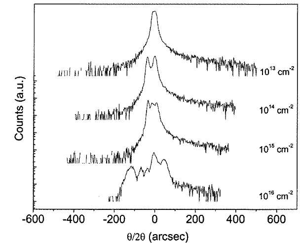
3.1. DCXRD of 1 MeV P ion implanted SI InP at 200°C as a function of dose
42
3.2. DCXRD for 1016 crri2 implant of 1 Me V P ions at 200°C and model (a); (b) strain
profile corresponding to simulated spectrum in 42
3.3. DCXRD of 3.3 MeV In ion implanted SI InP at 200°C at different doses
corresponding to the damage created by 1014, 1015 and 1016 cm·3 1 Me VP ion implants
3.4. X-ray rocking CUIVes from InP implanted with various ions at 200°C to a dose of 1016
cm"2.1 Me VP (a), 2MeV As (b), 2.1 Me V Ga (c) and 3.3 Me V In (d) .. ... 45 3.5. DCXRD spectra for (a) 2 Me V As and (b) 3.3 Me V In ion implanted InP at 200°C to a
dose of 1016 cm·' as a function of etch depth... 47
3.6. Cross sectional TIM images of As ion as-implanted (a) and annealed (b), Ga ion
as-implanted (c) and annealed (d), and In ion as-as-implanted (e) and annealed (t)
semi-insulating InP .... . 48
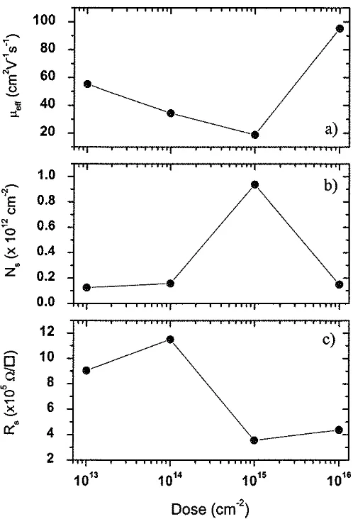
3.7. Effective mobility µ,ff (a), sheet carrier concentration
G
(b) and sheet resistance R, (c)as determined by Hall measurements and as a function of 1 Me V P ion dose for P ion
and 3 .3 Me V In ion implants at 200°C into SI InP. In ion doses calculated to give
equivalent levels of damage causes by P ion implants are also shown ... 51
3.8. Mobility (a), sheet carrier concentration (b) and sheet resistance (c) as a function of
annealing temperature, for P, As, Ga and In ion implanted SI InP 55
3.9. Ga ion implanted InP annealed at 600'C: (a) Representative SCM (dC/dV mode)
imageand (b) Representative SSRM image . 57
3.10. SSRM and SCM line scans obtained for the P ion implanted InP samples annealed at
400'\'.::, 500'(; and 600"C. (a) SSRM resistance profiles. (b) SCM profiles (de/ dV
mode)... 59
3.11. SSRM and SCM line scans obtained for the Ga ion implanted InP samples annealed at
400'\'.::, 500'(; and 600"C. (a) SSRM resistance profiles. (b) SCM profiles (de/ dV
mode)... 59
3.12. SSRM and SCM line scans obtained for the As ion implanted InP samples annealed at
400'\'.::, 500'(; and 600'C. (a) SSRM resistance profiles. (b) SCM profiles (de/ dV
3.13. SSRM and SCM line scans obtained for the In implanted InP samples annealed at
400"C, 500'C and 600'C. (a) SSRM resistance profiles. (b) SCM profiles (dC/ dV
mode) 60
3.14. Plot of time resolved photoluminescence decay times for p -InP ( - 3.4 x 1017 cm3)
implanted with different doses of 1 Me V P ions at 200°C ... 65
3.15. TRPL decay times measured at 300 K and simulated peak atomic displacements
(TRIM) produced for P, As, Ga and In ion implanted SI InP 67
3.16. dR/R signals of P ion implanted (a), and As ion implanted (b) samples annealed at
700°C ... 67
4.1. (a) Dose dependence of sheet resistance of p-InGaAs samples, irradiated with 2 MeV
C, 2 MeV 0, 0.7 MeV Li and 0.6 MeV Hions. (b) The estimated vacancies/ion/cm
calculated using TRIM vs critical dose obtained from data in (a), with a linear best
fu
n
4.2. {a) Dose dependence of sheet resistance of
p
-InGaAs samples with different initialfree electron carrier concentrations, irradiated with 2 Me V 0 ions. (b) Original free
carrier concentration of the samples vs critical dose obtained from data in (a), as well as
for similar implants done with 2 MeV C, 2 MeV 0 0.7 MeV Li and 0.6 MeV Hions
(including linear fits).... 79
4.3. Isochronal annealing stability of sheet resistance for
p
-InGaAs(p -
8 x 1017cm3 )
epilayers implanted at a range of doses above and below D0 for (a) 2 Me V 0, (b) 2
MeV C, (c) 0.7 MeVLi, and (d) 0.6 MeVHion implantation... 82
4.4. (a) Dose dependence of sheet resistance of n-InGaAs samples, irradiated with 2 MeV
calculated using TRIM vs critical dose obtained from data in (a), with a linear best
fu 85
4 .5. (a) Dose dependence of sheet resistance of n -InGaAs samples with different initial
free electron carrier concentrations, irradiated with 2 MeV C ions. (b) Original free
carrier concentration of the samples vs threshold dose obtained from data in (a) 86
4.6. Isochronal annealing stability of sheet resistance for n -InGaAs (n - 2.7 x 10¹⁷ cni3)
epilayers implanted at a range of doses above and below D0 for (a) 2 Me V 0, (b) 2
MeV C, (c) 0.7 MeVLi, and (d) 0.6 MeV Hionimplantation.... 87
5.1. Effective mobility, µclf> sheet carrier concentration, N, and sheet resistance R, as a
function of dose for 2 Me V Fe ion implantation into SI InP at 200°C, as determined by
Hall effect measurements 96
5.2. X-ray rocking curves as a function of dose for 2 Me V Fe ion implantation . 97
5.3. XIEM of Fe ion implanted InP to doses of 1014 and 1016 cni2 at 200°C 98
5.4. Dependence of effective mobility (a), sheet carrier concentration (b) and sheet
resistance (c) on annealing temperature for SI InP samples implanted with 2 Me V Fe
99
5.5. Photoluminescence transients for Fe ion implanted InP (dose: 1014 cm·~ annealed at
different temperatures. . 100
5.6. Arrhenius plot of the inverse PL decay time For Fe ion implanted and annealed InP
layers (circles). The squares show the data for the Pion implanted samples suggesting a
5.7. Mobility (a), sheet carrier concentration (b) and sheet resistance (c) as a function of P
ion implant dose, for p-type InP with hole concentrations -3.4 x 10¹⁷ and -1.3 x 10¹⁸
106
5.8. Effective mobility (a), sheet carrier concentration (b) and sheet resistance (c) as a
function of implantation dose for p -type InP implanted with 1 Me V P ions and
annealed at 500 and 600 °C, respectively ... 107
5. 9. PL decay times for P ion implanted InP samples annealed at 500 and 600°C as a
function of implantation dose 108
6.1. Effective mobility, µ,m sheet carrier concentration, N,, and sheet resistance, R,, for
both room temperature and 200°C 2 Me V Fe ion implantation as a function of
dose ... . 117
6.2. DCXRD of an unimplanted 1.5 µm InGaAs epilayer grown on a SI InP
substrate. 119
6.3. Evolution of X-ray rocking curves as a function of dose for room temperature
implantation of InGaAs epilayers with 2 Me V Fe ions . 119
6.4. XIEM scans for InGaAs epilayers on InP, implanted with 2 MeV Fe ions at room
1016
-temperature to cm .... 121
6.5. DCXRD of InGaAs implanted to 1016 cni2 at room temperature with 2 MeV Fe ions
and annealed at temperatures between 500°C and 900°C 122
6.6. XIEM image for InGaAs epilayers on InP implanted with 2 Me V Fe ions at room
1016 -2
temperature to cm ... . 122
6.7. Evolution of DCXRD spectra as a function of dose for 200°C implantation with 2
6.8. XTEM images for InGaAs epilayers on InP, (a) and (b) implanted with 2 MeV Fe ions
200°C to 1015 cm-2, and (c) and (d) to 1016 cm2 .... 124
6.9. DCXRD of InGaAs implanted to 1016 cm' at 200°C with 2 Me V Fe ions and annealed
at temperatures between 500°C and 900°C.... 126
6.10. XTEM images for InGaAs epilayers on InP, implanted with 2 Me V Fe ion 200°C to
1016 cm', and annealed at 800°C for 30 seconds 126
6.11. Effective mobility, µ,m and sheet resistance R, for room temperature 2 Me V Fe ion
implantation as a function of annealing temperature for 1015 and 1016
cm-2 . 128
6.12. (a) Measured and simulated TRPL traces from annealed InGaAs samples implanted at
room temperature with a dose of 1015cm-2
• (b) Differential reflectivity measurements of
the same samples excited with band gap energy photons 131
6.13. Effective mobility, µo11, sheet carrier concentration, N, and sheet resistance R, for p
-InGaAs implanted at room temperature with 1 Me V P ions as a function of dose and
for annealing at 500°C and 600°C for 60 seconds 135
6.14. X-ray rocking curves of room temperature 1 Me VP ionimplantedp-InGaAs to a dose
of 1016 cm-2 as a function of annealing temperature.. 136
6.15. Evolution of X-ray rocking curves for room temperature 1 MeV Pion implanted
p-InGaAs as a function of dose for (a) 500°C and (b) 600°C annealing for 60
seconds 136
7.1. Schematic of quantum well interdiffusion ....
7.2. Schematic of quantum well epitaxial structures used in the study ...
143
146
7.3. Vacancies produced by implanting into InGaAs epilayers on InP as a function of
7.4. Schematic of quantum well interdiffusion induced by ion implantation (low and high
energy cases depicted)... 14 7
7.5. 77K photoluminescence peak energy of InP/InGaAs quantum wells (with InP or
InGaAs cap) and InGaAs/ AlGalnAs quantum wells (with InP or InGaAs cap) as a
function of annealing temperature... 149
7.6. Low temperature (77K) photoluminescence spectra from InP/InGaAs quantum well
structure implanted at room temperature with 20 ke V P ions to various doses and rapid
thermally annealed at 700°C for 60 seconds ... . . 151
7.7. Energy shift of InP capped InP/InGaAs quantum wells as a function of dose for 20
ke V P ion cap implants at both room temperature and 200°C .... . 152
7.8. Energy shift of InGaAs capped InP/InGaAs quantum wells as a function of dose for
20 ke VP ion cap implants at both room temperature and 200°C ... . 152
7.9. Glancing angle RBS-C spectra for the InP capped sample, implanted with 20 ke V P
ions to a dose of 1014cm·2 at room temperature and 200°C. 153
7.10. Glancing
angle
RBS-C spectra for the InGaAs capped sample, implanted with 20 keVP ions to a dose of 1013 and 1014crri2 at room temperature and 200°C. 153
7.11. Energy shift of InP capped InGaAs/ AlGalnAs quantum wells as a function of dose
for 20 keV Pion cap implants at both room temperature and 200°G.. 157
7.12. Energy shift of InGaAs capped InGaAs/ AlGalnAs quantum wells as a function of
dose for 20 ke VP ion cap implants at both room temperature and 200°C... 157
7.13. Energy shifts of InGaAs/ AlinGaAs quantum wells as a function of dose for 20 ke VP
ion cap implants at room temperature, for different annealing temperatures and cap
7.14. Energy shifts of InGaAs/ AIInGaAs quantum wells as a function of dose for 20 keV P
ion cap implants at 200°C, for different annealing temperatures and cap layers 159
7.15. Energy shift as a function of dose for all quantum well samples after implants with 1
Me V P ions at 200°C and annealing at 700°C for two 60 second intervals .. 162
8.1. Schematic of interdiffusion induced byimputityfree vacancy disordering... . 169
8.2. Ground state (electron-heavy hole) transition energy variation with interdiffusion, for
various values of k = group
VI
group III diffusion rates ... 1718.3. Schematic illustrating concepts for 'single layer' and 'bilayer' impurity free vacancy
disordering . 172
8.4. 77K photoluminescence spectra of InGaAs capped InP/InGaAs quantum wells for
PECVD of 60 nm Si02 ... 175
8.5. Photoluminescence shifts as a result of SiO,!SiN, bilayer dielectric treatment of the
InGaAs capped InP/InGaAs quantum wells, with the Si02 thickness varying between
50 and 700
A
and an overlayer thickness of - 200nm, after annealing at 800°C for 60s.a) Photoluminescence spectra at 77K, b) Energy shifts as a function of Si02
thickness ... . 183
8.6. Photoluminescence shifts as a result of Si0,/Ti02 bilayer treatment of InGaAs capped
InP/InGaAs quantum wells, with the Si02 thickness varying between 5 and 70 nm and
an overlayer thickness of 200 nm, after annealing at 800°C for 60s. a)
Photoluminescence spectra at 77K, b) Energy shifts as a function of Si02
thickness 185
8.7. Photoluminescence shifts of InGaAs capped InP/InGaAs quantum wells coated with
8.8. XPS in-depth profiles of InGaAs capped InP/InGaAs quantum wells treated with an
undoped SOG 189
List of Tables
8.1 Thermal expansion coefficents for InGaAs, InP and GaAs and various
dielectrics ... 179
8.2 Photoluminescence energy shifts (in meV) for 200 nmPECVD deposited Si02, SiNx
Table of Acronyms
DCXRD k MOCVD PECVDPL
QW
RBS-CR.
RTA SCM SSRM SOGTRDR
TRPL
XPS
XTEMDouble crystal x- ray diffractomeny
ratio of gp V to gp III diffusion lengths
Metalorganic chemical vapor deposition
Effective mobility
Sheet carrier concentration
Plasma enhanced chemical vapor deposition
Photoluminescence
Quantum well
Rutherford backscattering-channeling spectrometry
Sheet resistance
Rapid thermal annealing
Scanning capacitance microscopy
Scanning spreading resistance microscopy
Spin-on glass
Time resolved differential reflectance
Time resolved photoluminescence
X-ray photoelectron spectroscopy
Publications related to this thesis
Journals
1. A wnparison
<f
irrpurity-fire am mirrplantatimirKiuarl intemixirrg<f
InGaAs/InP quantumwdls,L. V. Dao, M Gal, C Carmody, H H Tan, and C Jagadish, J. Appl. Phys. 88, 5252 (2000)
2. Ultrafast trappirrg tim5 in ion irrplanudlnP, C Carmody, H Boudinov, H H Tan, C Jagadish,
MJ. Lederer, V. Kolev, B. Luther-Davies, L. V. Dao, and M Gal,J. Appl. Phys. 92, 2420
(2002)
3. 7berrrdunin!scm::e inmirrplanud GaAs, M Gal, L.V. Dao, E. Kraft, MB.Johnston, C
Carmody, HH Tan and C Jagadish, J. Luminescence, 96, 287-293 (2002).
4. Irf/,ue=
<f
cap
lap on irrp/antation irKiuarl inrerdiffasion in InP /JnGaA s quantum wdls, CCarmody, H H Tan, and CJagadish,J. Appl. Phys. 93, 4468 (2003)
5. Ultrafast carrier trappirrg arr1 mmbination in hilf;ly nsistiie ion irrplam«l InP, C Carmody, H H Tan, C Jagadish, A Gaarder and S. Marcinkevicius, J. Appl. Phys, 94 (2003)
6. Ionlrrplam«llno.53Ga04,Asforultrafastoptak:trwicapp!U:ations, C Carmody, H H Tan, C
Jagadish, A Gaarder, and S. Marcinkevicius, Appl. Phys. Lett., 82, 3913 (2003)
7. Structural, Ekxtrical am Optical analysis
<f
ionirrplanudserri i.nsulatinglnP, C Carmody, H HTan, CJagadish, 0. Douheret, K. Maknys and S. Anand,]. Zou,L. Dao andM Gal.,
submitted to J. Appl. Phys. (2003)
8. Ekxtrical isdation
<f
n - amp - Ino,,3Ga0,,As epilaps usirrg ion irradiation, C Carmody, H HConference Proceedings
1. E Umical
am
optical propertifs if Me VA s and P ion inplant«l and anneakl ImiumPhaphide, C Carmody, H Boudinov, H H Tan, C Jagadish, M J. Lederer, V. Kolev and B.Luther-Davies, Proceedings of 2000 IEEE Semiconducting and Insulating Materials Conference,
IEEE Publishing Co., Piscataway,
NJ,
137 (2000)2. Use if Wn-inplantationfor the
creation
if ultrafast phctaleteaorrmterids and tuning if qua:atumwdlirframiphotaietertors, H H Tan, L. Fu, CY. Carmody and CJagadish, Proceedings of SPIE
Conference on Photodetectors: Materials and Devices VI, SPIE, San Jose, 47 (2001)
3. lan-inplant«llnP forultrafastphctaleteaorapplimtions, C Carmody, H Boudinov, H H Tan,
C Jagadish, L.V. Dao and M Gal, Proceedings of 2000 Conference on Optoelectronics
and Microelectronics Materials and Devices, IEEE Publishing Co. 153 (2001)
4. Irf/uem:!if cap fa:p-oninterdiffosioninlnP/IrlJaAs qua:atumwdls, C Carmody, H H Tan, and
C Jagadish, Proceedings of 15th Annual Meeting of the IEEE Lasers and Electro-Optics
Society, 2 , 845 (2002)
5. Euiutionq'JnGaAsllnPQ;amum WdllnternixirrgAs A FurKtinnCfCapLap, C Carmody,
H H Tan, CJagadish, Proceedings of 2002 Conference on Optoelectronics and
Microelectronics Materials and Devices, IEEE Publishing Co. (In press)
6. Stmaural, ElstricalAnd Optical Properties Cf MevAs+ Ionlnplant«llnP, C Carmody, H H
Tan, C Jagadish, J. Zou, L. Dao, M. Gal, Proceedings of 2002 Conference on
Optoelectronics and Microelectronics Materials and Devices, IEEE Publishing Co. (In
press)
7. Ultrafast canier trappirrg inhiffa
=w
ion inplant«l irrliumphaphide, C Carmody, H Boudinov,and Insulating Materials Conference, Bratislava, Slovakia, June 2002, IEEE Publishing Co.
GIAP1ER1
Recent developments in ill/V compound semiconductors have led to a revolution in
fast optical communications systems; new optoelectronic devices such as lasers,
modulators
and
photodetectors based on InP and InGaAs are widely used in both longand short haul communications networks. In these netwerks, of particular importance is
the demand for faster data transmission rates, which are needed for a range of
applications such as broad band internet and video on demand, and which require
devices which can operate at much faster rates. In order to meet this demand, twO main
technologies have been proposed; one is based on optical rime domain multiplexing,
and
the other on wavelength division multiplexing. The former technology achieves
increased data transmission rates by sending and receiving the optical signals at higher
frequencies. The latter produces the same effect by sending data at a slower rate, but
over a range of wavelengths. The studies in this Thesis address both these technologies,
using ion implantation and bandgap tuning techniques.
Although it may defy common sense, adding imperfections to semiconductors
can actually improve their performance in devices used for everything from information
technology to playing music. Creating defects on pmpose
(defect
engineering)- or puttingnaturally occurring defects to good use - can have major implications for the future of
Optoelectronics and materials science.
Of the III/V semiconductors, InP and InGaAs are preferred for long
-wavelength optoelectronic applications. Moreover, it is logical to study these materials in
conjunction, since InGaAs layers are inevitably grown lattice matched to InP substrates.
At, room temperature, and with InGaAs lattice matched to InP (corresponding to a
translates to emission/ detection wavelengths of - 0.9 and 1.6 µm. Apart from the
epitaxial layers, heterostructures can be made from these semiconductors with
emission/ detection wavelengths in the highly desirable 1.3 and 1.55 µm range, which is
the operating wavelength used in long haul optical fibre communications.
The study into defects in InP and InGaAs offered here represents a contribution
to the ongoing efforts into uncovering new ways of controlling, or even exploiring, these
defects for optoelectronic device applications. The defects were created primarily by ion
implantation, while a small section of work deals with defect injection via deposition of
dielectric layers on the surface of samples. There are two main directions this work has
taken. Firstly, the defects created by ion implantation are studied as causes of electrical
and optical characteristics which, in bulk InP and InGaAs, could be very useful in
fabricating devices with very fast optical response times that could be employed in
increased bandwidth optical fibre communications, not to mention ultrafast long
wavelength spectroscopic techniques. When a crystalline semiconductor is ion
implanted, the incoming charged atom undergoes a series of collisions with elements in
the target, causing cascades of 'knock on' collisions which dislodge target atoms from
their usual lattice positions. As such, these 'out of place' atoms are defects which bond
with the surrounding atoms in a variety of ways, existing as simple
point
d(ffi:S such asvacancies, interstitials or antisites, or forming more complex clusters, loops, stacking
faults or voids. Each of these defects have their own optical and electrical characteristics
- they may act as carrier traps or donate excess carriers to the semiconductor - with
energy levels that can exist in the valence or conduction band or within the band gap.
also, they induce strain into the matrix due to deviations from the usual Janice
configuration. In large enough concentrations, they can v:uythese characteristics enough
to modify the properties of an entire sample and be observable in optical and electrical
experiments and also experiments which reveal the structural integrity of the material
Secondly, the defects in these materials are used to drive a process called
interdiffasm
in InP and InGaAs based quantum wells, which means an exchange ofelements at InP/InGaAs interfaces. This is a method which has been used to 'tune'
emission/ detection wavelengths in lasers and photodetectors made out of quantum
semiconductor structures, and has been investigated for monolithic integration of
optoelectronic devices. Point defects mentioned above are
ideal
for interdiffusion, sincethey are highly mobile in the semiconductor at elevated temperatures, and can diffuse
large distances within a sample. In this way, they promote an exchange of elements
across interfaces between two semiconductors. In the case of quantum wells, this results
in a smoothing of the semiconductor composition across what was initially an abrupt
interface, which also causes a smooth variation in bandgap where previously there was a
shaip step between the adjacent materials. Thus, the shaip square potential of a
quantum well can be modified, which leads to changes in the energy levels
within
thequantum well, and ultimately its emission/ detection wavelength.
Oiapter 2 discusses the various methods which vvere used to fabricate and
modify samples, as well as the experimental techniques employed to assess the changes
to the electrical, optical and structural properties of the material. Oiapter 3 presents
detailed investigations into the properties of ion implanted semi-insulating InP, and raises
4 discusses similar studies into the electrical properties of ion implanted InGaAs
epilayers grown on InP substrates, and focuses in particular on methods of achieving
electrical isolation in this material using the damage caused by the implantations. In
these two chapters, the similarities as well as the differences of defective InP and InGaAs
become apparent. Efforts to modify the properties of these materials are then described
in the following Chapters. Chapter 5 looks at methods of obtaining implanted InP
suitable for ultrafast optoelectronic applications, and Chapter 6 details similar studies
using epitaxial InGaAs. In Chapter 7 and 8, the defects are put to a different use in
promoting interdiffusion studies in InP/InGaAs and InGaAs/ AlGainAs quantum well
structures. In the former Chapter, interdiffusion is driven by defects resulting from ion
implantation, and in the latter, dielectric layer deposition is investigated as an equally
powerful means for achieving tuning of emission/ detection wavelengths of quantum
structures made from InP and InGaAs. Finally, Chapter 9 details the main conclusions,
GIAP1ER2
2.1 Introduction
The experimental techniques used for both fabrication and analysis of samples studied in this
Thesis will be presented here. Descriptions are restricted to providing a basic understanding
of the methods and equipment employed, since a more comprehensive picture is best sought
in the references provided at the end of this Chapter. Issues relating to each technique that are
of particular interest to this Thesis will be covered in more detail in the appropriate sections.
The main techniques have been categorized as follows
• Epita:xial growth (sample fabrication)
• Ion implantation and sample processing (sample modification)
• Material characterization (structural, electrical and optical analysis of samples)
2.2 Epitaxial Growth
The InP and InGaAs epilayers as well as quantum well structures used in this work were all
grovm by metalorganic chemical vapour deposition (.MCXND). MCXND is a thin film
deposition process using a vapour phase reaction between metalorganic compounds of the
group III elements and hydrides of the group V elements; a detailed description of the
processes involved can be found in several good books and reviews1
•4• All samples were
grown at the Australian National University using an AIXTRON AIX 200/ 4 horizontal flow
(with rotation) reactor. The growth temperature was 650°C, pressure was 180 mb, and the
Technology. P-type as well as n ·type InP and InGaAs epilayers were grown by doping with
Zn and Si, respectively. InGaAs was always grown with a nominal In composition of 53%
and Ga composition of 47% such that the epilayers were lattice matched to the InP substrates.
AIInGaAs used in quantum well structures in Oiapter 7 used an Al composition of 20%, Ga
composition of 27% and In composition of 53% for the same reason.
A summary of the structures used in this work is as follows:
Oiapter3:
Oiapter4:
Oiapter5:
Oiapter6:
Oiapter7:
Oiapter8:
InP semi-insulating (SI) substrates; undoped InP epilayers on n+InP
substrates;
p ·
InP epilayers on SI substrates.n · and p · type InGaAs epilayers
InP SI and p • type epilayers
undoped and
p ·
type InGaAs epilayersInP /InGaAs quantum wells with InP or InGaAs capping layers;
AIGainAs/InGaAs quantum wells ·with the same capping layers
InP/InGaAs quantum \veils with InGaAs capping layers
More detailed descriptions of the samples are provided in the experimental section of
each Oiapter.
2.3 Sample Processing
2.3.1
Ion Implantation
Ion implantations-7 involves the irradiation of samples with ioniz.ed atoms (i.e. ions) which can
be accelerated to energies from a few ke V to several Me V. Soch energetic ions, upon impact,
lose their energy via a series of collisions with target noclei and electrons. These collisions can
result in displacements of atoms in the target, leaving lattice defects in cry:;ralline solids. Such
defects constitute the main focus of thi~ work
Ion ranges and atomic displacements produced by ion implantation can be calculated
using
Trans
port of Ions in Matter (TRIM) monte carlo simulations8• Implantation produces
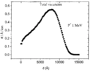
Gaussian-like (unimodal) damage (atomic displacement) profiles, as shown in Figure 2.1. The
thickness of
the
layer altered bythe
implantation as \vell as the number of atomicdisplacements generated depends on ion mass and energy. Generally speaking, the greater the
ion mass, the more damage is created. The TRIM code takes into account only ballistic
processes and ignores effects such as dynarric anmding (defect migration and interaction
processes). Moreover, this code does not have any scope for predicting
the
damage profilesTotal vacancies
5000
d (A)
•
"
\ P+ I MeV\
•
•
\__
[image:35.595.142.459.474.728.2]when implants are done at temperatures other than room temperature. Thus,
actual
damagecaused in the sample by implantation must be verified experimentally. However, we have
found that the depth of the maxim= damage predicted by
TRIM
corresponds v.11ill to thevalues measured for implants into InP and InGaAs at elevated temperatures.
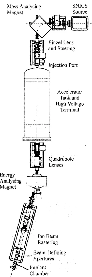
Experimental Details
In this work, ion implantation was performed on both the low and high energy ion implanters.
Figure 2.2 shows a schematic of the ANO 1.7 MV tandem accelerator
(NEC,
SSDH-4) usedfor high energy implants. Samples were mounted on the target holder in the implant chamber
using metal clips. The ion soun:e is a SNI
a; -
type, (Source of Negative Ions by Cesi1.UllSputtering) where a stream of Cs vapour
is
ionised into Cs- which are then attracted to anegatively biased cathode (~ 10 kV). The ions to be implanted are nonually obtained from a powder source which is pressed into a Ch cathode. The
list
below shows (in order ofincreasing atomic mass) the source materials for the various ion species used.
Ions Atomic Mass (a.m.u/ Source Material
H 1.00 TiH2powder
Li 6.94 LiOH pov.tder
c
12.01 Carbon pov.'<ier0 16.00 Al103 powder
p 30.97 Gushed InP wafer
Fe 55.85 Solid machined steel cathode
Ga 69.72 Ga203 powder
As 74.92 Gushed GaAs wafer
Mass Analysing SNlCS Source
Magnet i
Energy
Analysing Magnet
B
and Steering
I
----'~~~~~~
---1---1
I
i
I
---1---_____ T ---1---_____ .
I
Accelerator
Tank and High Voltage
Terminal
Quadrupole
Lenses
Ion Beam Rastering
Beam-Defining
Apertures
Implant Chamber
[image:37.595.214.395.106.649.2]The positively-biased extractor (s 15 kV) then attracts the sputtered negative ions, accelerating
them further by a bias (580 kV) into a 90" magnet, with a path radius R, for mass-filtering. By
setting the magnetic field such that the magnetic force acting on the accelerating ions is equal
to the centripetal force of the ions as they are deflected through a radius (R), the required ions
with mass (m) and charge (n) will be singled out by being deflected tow:utls the high voltage
tenninal, i.e.
B = l!R-{ 2mV; I qn [2.11
where B is the magnetic field, V, is the potential of the ions and q is the electronic charge.
The high voltage terminal resides in the middle of a tank containing pressurised SF 6 gas
for insulation purposes. Positive charge (up to 1.7 MV) is supplied to the terminal by two
pelletron chains. The voltage applied to the high voltage terminal is sustained through a series
of equi·potential rings separated by resistors, as the beam path at the two ends of the tank are
kept at ground potential The voltage stability of the terminal is ensured using a set of corona
points which form a closed loop feedback system. The mass-filtered negative ions coming
from the 90" magnet are electrostatically steered into the tank and accelerated tow:utls the
positive high voltage terminal At
this
terminal, they are partially stripped of electrons in anitrogen charge-exchange cell to become positive ions and as a result are further accelerated
tow:utls the other end of the tank (at ground potential). Thus, the final energy, Vr, of the ions
1S
where V, is the voltage at the terminal,
v,
is the injected potential of the ions and n is thecharge state of the ions. Typically, the final ion energy is in the range 0.2 - 10 MeV. If lower
energies are required
($;
150 keV), the low energy ion implanter is used, which operates on asimilar principle to the source end of the high energy implanter.
2.3.2
Rapid Thermal Annealing (RTA)
Rapid thermal annealing10 is a crucial step in preparing samples for all aspects of this v:10rk. By
annealing at different temperatures and times one can learn a great deal about the
thermal
stability and mobility of defects in semiconductots. Besides, high temperature process steps
are part and parcel of the device fabrication techniques, and so were used routinely in this
v.'Drk. Annealing steps were also used to promote interdiffusion and damage removal All the
RTA processes were performed in an Ar ambient with temperature ramping at 100°CI s, were
done in the proximity geometry, where samples were covered with sacrificial material to
minimize material decomposition. For example, P has a strong tendency to evaporate from
InP at annealing temperatures above 400°C, thus it is necessary to use sacrificial pieces of InP
to maintain the P vapour pressure at the surface. Where InGaAs surfaces were concerned,
sacrificial GaAs was used to prevent excess loss of As.
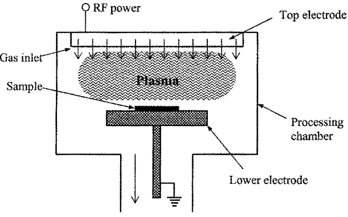
2.3.3
Plasma Enhanced Chemical Vapor Deposition (PECVD)
It was necessary to deposit dielectric layers of Si02 and/ or SiN, for the intermixing studies
RF power
Gas inle
1
Top electrode
Processing chamber
[image:40.595.130.469.104.316.2]Lower electrode
Figure 2.3 Configuration of the PECVD system. Courtesy of Dr. L. Fu.
PECVD uses the principle of nonequilibrium glow discharge11
, which is defined as a
partially ionized gas containing equal volume concentrations of positively and negatively
charged particles (mostly ions and electrons, respectivel0 existing in different concentrations
of ground-state and excited states"'. Nonequilibrium glow discharges are generated by
subjecting the gas to a radio frequency (RF)
electric
field. The small concentration of freeelectrons initially present in the gas are accelerated by
this
electric field. Ar. sufficiently highenergies, the electron collisions with atoms in the gas excite and ionize them, in the latter case
creating additional electrons which are also accelerated by the electric field. In
this
way anavalanche of accelerated electrons creates a steady state glow discharge. Ar. steady state, a
fraction of the ground-state parent atoms in the gas phase undergoes electron impact
dissociation and excitation such that
highly
reactive species are created, which in turn diffusemigration, and eventually form a solid film. Since the reactive species produced in the plasma
have lower energy barriers to physical and chemical reactions than the parent species, they can
react at lower temperatures, which is the major advantage of PECVD compared with other
thin film deposition techniques.
The plasma is generated between two parallel, circular electrodes, with the sample
being placed on the lower, electrically grounded electrode. The upper electrode is con.nected
to a 13.56 MHZ RF generator and the reactantS ( Sili., NH3 and N20 gases) are fed in from
the gas inlet through the top electrode, entering the plasma region. The gases used were 5%
silane (in Ni) and nitrous oxide for Si02 deposition and 5% silane (in Ni) and ammonia for
Si.N,. deposition.
2.3.4
Electron Beam Evaporation
Another method of forming films on the surface of samples is by electron beam evaporation.
In this case, the heating of the material to be deposited is done using a focused beam of electrons, which has the advantage of being able to heat to very high temperatures a small
region of the source material to such high temperatures that it evaporates. The material then
recondenses on all the surfaces of the evaporation chamber, including on exposed
samples.Tio,, a dielectric used for interdiffusion studies in Chapter 8, was evaporated onto
samples via this technique using a Temescal CV-8 electron beam evaporator.
2.3.5
Spin-on Glasses (SOGs)
Spin on glasses are another form of silica which can be deposited on the surface of samples.
sample using standard spin deposition techniques. Then the sample is baked for a reasonable
time (such as 15 minutes) so that the solvent evaporates, leaving behind the amorphous silica.
Different baking temperatures result in a different quality (e.g. porositJ? of the silica. In this
work, spin on glasses were used in addition to the other dielectric deposition techniques to
promote interdiffusion in the quantum well samples. Undoped as well as P , Ga and Ti
-doped spin on glasses were used.
2.4 Material Characterisation
2.4.1
Double Crystal X-ray Diffractometcy (DCXRD)
DCXRD is a non-destructive technique widely used for measurements of compositions, layer
thickness and strain in epitaxial structures13
'14• In this work its use has primarily been to gauge
the strain profile introduced into epilayers as a result of ion implantation. A Bede QC2a
diffractometer was used, where a beam of Cu Ka X-rays is collimated to a reference crystal of
the same material and orientation as the specimen which also acts as a monochromator.
When the planes of the specimens are parallel to those of the reference crystal, Bragg
conditions are satisfied, i.e.
nA.=2dsin0a [2.3]
where d is the spacing of the Bragg planes, A. is the X-ray wavelength, 8B is the Bragg angle
(31.668° for (004) InP) and n is the order of diffraction (n=l, 2,. .. ). A slit is positioned in
slits
x-ray source
reference crystal (004)
Tocking' axis
detector
slits
specimen (004)
Figure 2.4 Schematic of a double-crystal X-ray diffractometer (DCXRD).
Courtesy Dr. H. H. Tan.
rotation of the specimen with respect to the reference crystal
will
result in a loss of intensityfrom the substrate. For one of the implanted samples, Dr. Manuela Buda at the Department of
Electronic Engineering,
Mu,
kindly performed modeling using the Takagi-Taupin Theory15 •2.4.2
Cross· sectional Transmission Electron Microscopy (XfEM)
Cross-sectional transmission electron microscopy (XTEM) is a well established technique to
study defects and microstructure of materials. It is rourinelyused to image and analyse damage
and defects in ion implanted materials. An XTEM sample may be investigated in several
modes, most commonly the diffraction
mode
(such as selected area diffraction and convergentbeam diffraction) and imaging mode (such as bright-field, dark-field and -weak beam imaging).
These methods allow a vast array of crystalline defects to be imaged and analysed. Details of
may be found in several good publications1"'18• XTEM analyses were canied out by Dr. Zou
Jin at the Electron Microscope Unit at the University of Sydney. Samples were prepared by
mechanical grinding followed by ion-beam thinning and then examined in a Philips CM 12
operating at 120 kV.
2.4.3
Ruthenord Backscattering-Channeling Spectrometry (RBS-C)
Rntherford backscattering spectrometty (RBS) is a quantitative ion beam analysis technique,
commonly used to analyse structural damage and composition of target samples. With this
technique, a beam of monoenergetic light ions (such as H or He) is bombarded onto the
specimen to be analysed. The backscattered ions are then collected and analysed for their
energy distribution which will yield information about the atomic constituents and also a depth
profile of the target. If the incident ions are aligned along a low index crystallographic
direction of a crystalline target (axial channeling), then most of the ions are steered into the
'channels' of the crystal, causing a significantly reduced backscattered ion yield. On the other hand, if the target is randomly oriented with respect to the incident ions, then fewer ions are
channeled along the crystallographic axes and more direct scattering will occur. The aligned
technique is generally referred to as ion channeling or RBS-channeling (RBS-Q. If defects are
present in the sample, such as displaced atoms in the channeling paths, then
the
yield of thebackscattered ions will increase. In this way, the channeling spectrum can give a depth and
concentration profile of defects present in the material, and is ideal for analysis of crystalline
x •···
···~-->-GaAs : crystal
incident ions
detector
Figure 2.5 Schematic representation of the backscattering process for a specific geometry.
The RBS-C measurements done in this Thesis were conducted on an ANU 1.7 MV
tandem accelerator (National Electrostatics Cotporation, U.S.A, model SSDH), which has a
similar design to the 1.7 MV implanter depicted in Figure 2.2. In this case, a rubidium ion
source is used (not a SNI CS) and a high voltage tank with only one nylon chain.
The geomeuy of the RBS detection Sj"Stem is important in the quantitative analysis of
the results, such as the depth profile. The energy loss of an incident ion with energy E0 in
traversing a distance x from the surface and backscattered by a P atom is related to the
following expression, as illustrated in Figure 2.5
s
=.!i.t_
dEI
+__!___
dEI
[]P cos (}dx"' (}dxout1 cos 2
[2.5]
where Kp is the kinematic factor of P, E1,P is the energy of the ion backscattered off a P atom
at x, [SJ,, is the energy loss factor of P and dE/ dx
I;.
and dE/ dxI
out are the rate of energy lossevaluated at the inward and outward paths, respectively. For regions near the surface, the
depth x is small and hence, the relative change of the ion energy along an incident path is also
small. Thus, it is sufficient to use a surface energy approximation which reduces the latter
expression to
Kp dEI 1
dEI
[S]p=--- + .
-cos(} dx E. COS(} dx K.oE.
1 2
[2.6]
Similar expressions are true for an ion scattering off an In atom. Further treatment of RBS
and ion channeling can be fOUlld in references 19 and 20.
2.4.4
X-ray Photoelectron Spectroscopy
X-ray photoelectron spectroscopy (XPS)21~2
operates on the principle irradiation of a sample
under vacuum with rnonoenergetic soft X-rays (t)pically Mg Ka (1253.6 eV) or Al Ka (1486.6
e V) produced by electron bombardment of Mg or Al targets), which interact v;,1th the surface
atoms such that electrons are emitted by
the
photoelectric effect. An electron spectrometercollects the photoelectrons and analyses their energy. The kinetic energy of an emitted
Figure 2.6 Schematic of the basic appararus used in X-ray photoelectron spectroscopy. X-rays are produced at
the
Al anode by bombardmem of electrons created at the filament. The X-rays impinge on a sample producing photoelectrons which are detected after analysis in the electron energy analyzer.21electron in the target atom. Because each element has a unique set of binding energies, XPS
can
be
used to identify and determine the concentration of elements in the surface. Variationsin the elemental binding energies (chemical shifts) are caused by differences in the chemical
potential and polarizability of
the
compounds inthe
sample,and
allow identification ofthe
chemical state of the elements in
the
sample. .Measurements were carried out by Dr. Bill BinGong at
the
University of New South Wales, on a ESCALAB220i-XL (VG Scientific, UK)X-ray photoelectron spectrometer. Standard conditions used a vacuum better than 2 x 10·9
mbar.
The
source used a monochromated Al Ku beam, with source power 10 kV x 12 mA = 120 W.The spot size was -0.5 mm across and
the
pass energy was 100 eV for wide scans and 40 eVfor narrow scans (resulting in depth profiles). The Ar ion beam used for sputtering into
samples (thus providing depth profiles) had an energy of 5 keV. Samples were analysed as
2.4.5
Sheet
Resistance
Sheet resistance (RJ is the resistance between the opposite edges of a square of arbitrary
dimensions. Sheet resistance is independent of the size of the square and is determined by
material resistivity and sample thickness. Thus, R, is a property of the sheet. For R,
measurements, rectangular samples were cut from InP and InGaAs-on-InP wafers. On two
opposite sides of each sample, ohmic contacts were fabricated. In the case of both InP and
InGaAs, it is relatively easy to
make
ohmic contacts: indium wire is pressed onto the surfaceand then the sample heated at 200°C until the metal is observed to have melted
and
oxidized(indicating a reai.1:ion with the semiconductor surface). Sheet resistance measurements of ion
implanted InGaAs were done
in
situ (without breaking vacuum in the target chamber of theimplanter) \Vith a specially designed sample holder. Measurements "l'V-ere performed several
minutes after each ion dose had been delivered.
2.4.6
Hall Effect
Htll
effect'', as a characterization tool, has been used throughout the history ofsemiconductors to provide a direct measure of free carrier type and density, and, 'lvhen
combined with a resistivity measurement on the same sample, carrier mobility. A standard
explanation of the physics of the
Htll
effect uses a uniform bar sample, as shown in Figure 2.6,where positive carriers flow under the influence of an electric field ~z along the bar. A uniform magnetic field B, is applied normal to the top surface, resulting in a force FB = eBxv,, which
Figure 2.6 Schematic diagram to illustrate the Hill effeet on a semiconductor
sample in the form of a "Hill bar". In (a) the coordinate system is defined and the forces aeting on positive holes which flow from left to right under the influence of
an applied electric field I;, are shown. The magnetic field B, is applied normal to the
sample surface and to the direction of current flow. In (b) we show the plan view of a practical sample with side arms A and B which are used to measure the applied
field I;, and C and D which allow measurement of the Hill field S,. Taken from Blood et aL 23
Since the Hall field!;, is proportional to both Bx and the current density Jz:
which can be rewritten as
RH=
=-v_,
=-IB,J, J, ne [2.9]
using equations [2.7] and [2.8] as well as the relation Jz =env,. The proportionality constant
RH is known as the
Hill
coefficient. TheHill
mobility µH can be expressed as[2.10]
where the resistivity is l/cr, land hare the length and width of the bar as sho¥.n in Figure
2.6, and V, is the voltage measured at contact x =A, B, C, or D.
In practice, averages of the voltage differences are obtained for both current directions
(when measuring RH) and magnetic field, in order to minimize errors. Although the bar
sample ensures a uniform current distribution and a well-defined electric field, the majority of
Hill
effect measurements are made in the van der Pauw24 geometry. :Measurements using thisconfiguration require far less geometrical accuracy than in the bar sample. The van der Pauw
configuration used in this work, consisting of four ohmic contacts placed in the comers of a
- 5 x 5 mm2 sample is illustrated in Figure 2.7. Van der Pauw published a theorem in 1958
which applies to the measurement of resistivity in a sample of uniform thickness and doping
level but otherwise of arbitrary shape, where four contacts A, B, C and D are placed along its
o.
.. c
•
..
A B
Figure 2.7 Schematic diagram to illustrate the van der Pauw configuration with ohmic contacts A, B, C and D.
[2.11]
where V fill is the voltage measured between contacts A and B when a current Im is passed
between C and D. Van der Pauw also showed that the Hall coefficient is given by:
[2.12]
where !iRBD.<c is the change in RBDAc produced by applied magnetic field Bx ( RBDAC is
measured using diagonal pairs of contacts rather than adjacent pairs). It is standard practice to
reverse the current and magnetic field and interchange current and voltage contacts, obtaining
2.4.7
Scanning Spreading Resistance Microscopy (SSRM)
Scanning Probe Microscopy based electrical characterisation methods have emerged as
promising techniques for two-dimensional mapping of electrical properties at the nanometer
scale". Application of Scanning Capacitance :Microscopy (SCM) and Scanning Spreading
Resistance :Microscopy for characterisation of both Si and III-V based materials
and
devices,has already been reported2
"30• The obtainable lateral resolution (20-SOnm) is cypical of probe
tips diameter used in Atomic Force :Microscopy (AFM). SCM and SSRM are complementary
techniques and very well suited to characterisation of electrical properties of ion implanted
InP. Patticularly, investigation of sample cross-sections provides such information at different
locations.
In scanning spreading resistance microscop:f3~1,
an electrical resistance is measured
between a conductive probe tip and a large current-collecting back contact while the probe is
scanned in the contact mode across the cross section of the sample. \X?hen the applied force
exceeds a certain threshold force, the measured resistance is dominated by
the
spreadingresistance. This resistance R,, associated with a single probe of contact radius a, results from
current crowding close to the contact region in the semiconductor; R, is therefore determined
by
the
resistivity p of a small volume of material within a hemisphere of radius - 2a. For a plane, uniform contactmaking
perfect ohmic contact at the surface of a semi-infinitesemiconductor,
In practice, real contacts form a potential barrier Rt, at the probe-semiconductor
interface, thus
Re = (R, + Rt,) =kp/4a, [2.14]
where the factor k is a slowly varying function of p which must be calibrated for each
individual probe. The spreading resistance depends inverse proportionally on the local cartier
concentration underneath the probe-sample contact. The SSRM measurements presented in
this
work
were performed with a Digital Instruments Nanoscope Dim 3100 microscopeequipped -with a SSRM module by Kestas Mastutis at
the
Department of Microelectronics andInformation Technology, Roy.tl Institute of Technology, Sweden. Oimmercial Boron-doped
diamond coated tips (NanoSensors GmBH) were used. Sample cross-sections were obtained
by manual cleaving. The current was measured using a logarithmic amplifier -with the de bias
applied to
the
sample. In this case, the samples consisted of epitaxial InP, about 1.5 µ.rn thick,gro'l>n on n+ InP substrates, which w-ere subsequently implanted -with the different ion-species.
2.4.8
Scanning Capacitance Microscopy(SCM)
In a scanning capacitance microscope31
, a tip (such as is used in atomic force microscopy} is
covered with a
thin
dielectric layer such that the tip-sample contact forms ametal-insulator-semiconductor (MIS) capacitor, whose capacitance voltage behaviour is determined by the