1Li–Fi R&D Centre, the University of Edinburgh, Institute for Digital Communications,
King’s Buildings, Mayfield Road, Edinburgh, EH9 3JL, UK
2Institute of Photonics, Department of Physics, University of Strathclyde, Glasgow G1 1RD, UK
3School of Engineering, University of Glasgow, Glasgow G12 8LT, UK
4Centre for Advanced Photonics and Electronics,
Electrical Engineering Division, Department of Engineering, University of Cambridge, Cambridge CB3 0FA, UK
compiled: February 21, 2017
Visible light communication (VLC) is a promising solution to the increasing demands for wireless connectivity. Micro-sized Gallium Nitride (GaN) light emitting diodes (mirco-LEDs) are strong candidates for VLC due to their high bandwidths. Segmented violet mirco-LEDs are reported in this work with electrical-to-optical bandwidths up to 655 MHz. An orthogonal frequency division multiplexing (OFDM) based VLC system with adaptive bit and energy loading is demonstrated and a data transmission rate of 11.95 Gb/s is achieved with a violet mirco-LED, when the nonlinear distortion of the mirco-LED is the dominant noise source of the VLC system. A record 7.91 Gb/s data transmission rate is reported below the forward error correction threshold using a single pixel of the segmented array when all the noise sources of the VLC system are present.
OCIS codes: (060.4510) Optical communications; (060.2605) Free-space optical communication; (230.3670) Light-emitting diodes; (230.3990) Micro-optical devices.
http://dx.doi.org/10.1364/XX.99.099999
1. Introduction
The increasing demands of communication services are challenging radio frequency (RF) wireless communica-tions technologies. The overall number of networked de-vices is expected to reach 26.3 billion in 2020 [1]. Visible light communication (VLC) is a promising solution to the limited availability of the RF spectrum as the vis-ible light spectrum offers abundant bandwidth that is unlicensed and free to use. VLC improves the spectral efficiency per unit area, which enhances the quality of service in crowded environments and allows for secure and localized services to be provided.
General lighting is under a rapid transformation to be-come semiconductor based due to huge energy savings. This transformation has already enabled applications such as active energy consumption control and color tun-ing. Solid state lighting devices such as Gallium Nitride
∗Contributed equally to this work. Corresponding author: [email protected]
(GaN)-based inorganic light emitting diodes (LEDs) are ubiquitous power-efficient devices to enable illumina-tion and communicaillumina-tions. Commercially available LEDs have a limited frequency response due to the yellow phosphor coating on top of the blue LEDs chips. How-ever, the slow response of the yellow phosphor can be filtered out using a blue filter in front of the receiver. Re-cent results for VLC using a phosphoresRe-cent white LED with adaptive bit and energy loading were reported at 2.32 Gb/s aided by a two-staged linear software equal-izer [2].
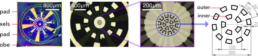
Fig. 1. Plan view micrographs of the segmented micro-LED arrays. The magnified micrographs on the right show the array configuration and individual pixel design. A diagram is also included noting inner and outer pixels (dimensions in micron).
3 Gb/s [6], and more recently a single pixel of a new seg-mented array has demonstrated 5 Gb/s [7]. The novel micro-LEDs emitting at 400 nm featured in the current work offer a number of advantages over the 450 nm de-vices previously reported [7]. From typical trends con-cerning the internal quantum efficiency (IQE) of indium gallium nitride-based active regions, comparable IQEs are expected at 400 nm and 450 nm, whereas IQE de-creases steeply at shorter emission wavelengths [8]. For generation of white light for illumination, use of violet-emitting LEDs exciting tricolour (red, green, blue) phos-phors also offers advantages over the widely used method of combining blue direct LED emission with a yellow-emitting phosphor. These include much superior colour rendering indices [9, 10], and the absence of a direct blue component, which has proven to be disruptive to the human circadian rhythm [11]. The micro-LED die shapes employed in this work are also expected to be ad-vantageous for efficient light extraction, by analogy with previous designs employing non-circular emitting areas [12].
VLC is enabled by incoherent illumination from the light sources. Therefore, only real and positive modu-lating waveforms can be realized. Single carrier mod-ulation schemes such as on-off keying (OOK), pulse amplitude modulation (PAM), and pulse width modu-lation (PWM) are straightforward to be implemented. However, the performance of these modulation schemes degrades as the transmission speed increases due to the increased inter-symbol interference (ISI). Equalization techniques can be used to improve the system perfor-mance at significant computation cost [13]. Multi-carrier modulation techniques such as orthogonal frequency di-vision multiplexing (OFDM) are promising candidates for VLC. Computationally efficient single-tap equaliz-ers are straightforward to be realized in OFDM. Adap-tive bit and energy loading in OFDM allows the channel utilization to approach the information capacity limit. In addition, multiple access can be easily supported in OFDM by assigning groups of sub-carriers to multiple users, which is known as orthogonal frequency division multiple access (OFDMA).
Previously, a 40µm diameter micro-LED at 405 nm
achieved a data rate of 3.32 Gb/s at an optical power of 2.5 mW with electrical–optical bandwidth up to
307 MHz [14]. In this paper, we present a high band-width VLC link at 400 nm. The emitter consists of a single pixel of the segmented micro-LED array design introduced in [7]. This device achieves 2.3 mW of opti-cal output power while maintaining an E-O bandwidth of 655 MHz. A VLC system is realized with a mod-ulation bandwidth of 1.81 GHz, evaluated beyond the 3 dB bandwidth of the system. Transmission rate of 11.95 Gb/s is presented, when the nonlinear distortion noise of the micro-LED is the major source of noise in the system. A record transmission rate at 7.91 Gb/s is presented when all the noise sources of the VLC system are considered.
2. Violet Micro–LED 2.A. Design and Fabrication
The design of standard GaN LEDs is based on a large-area chip assembled on a package that maximises heat extraction through an n-pad at the bottom for a flip-chip configuration. This creates two limitations: a large capacitance due to the package contact area and an up-per limit on the current density due to the rapid self heating of a large-area chip. The design and fabrication process of the micro-LED array used in this work are as reported in our previous work [7]. It consists of two circular micro-LED arrays, an inner and outer, contain-ing 5 and 10 pixels, respectively. Originally designed to match the geometry of plastic optical fibre, the inner and outer pixels have active areas of 435µm2 and 465µm2,
respectively. This compares with 1256µm2 active area
for the 405 nm device in [14]. Fig. 1 shows optical im-ages of this micro-LED array, together with a schematic of the pixel layout.
The wafer used in this work is for commercially avail-able GaN-based LEDs emitting at 400 nm. In order to fabricate these arrays, micro-LEDs emitters are etched by inductively coupled plasma to expose n-type GaN. An annealedPdlayer is used as metal contact to p-type GaN. Each emitter is isolated by a layer of SiO2. The
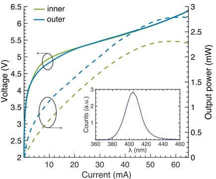
re-Fig. 2. Combined current-voltage (I-V), left, and luminescence-current (L-I), right, characteristics of both in-ner and outer pixels. The inset shows the emission spectrum of an inner pixel at 50 mA.
duction in performance due to mutual heating between pixels. The low optical power per pixel in micro-LEDs is a challenge when combined illumination and commu-nication is considered. This problem can be addressed by using large arrays of pixels, where a system capable of handing the communication link over multiple pixels can be designed to reduce duty cycle, reduce junction temperature on individual pixels and maintain high effi-ciency. These investigations are subject to future work.
2.B. Performance Measurements
The electrical performance of the micro-LED arrays was measured by a semiconductor analyser (HP 4155). The optical power of the arrays under direct current (DC) conditions was measured using a Si detector placed in close proximity to the polished sapphire substrate. A spectrometer and charge coupled device detection sys-tem was used for the collection of electroluminescence spectra. The small signal frequency response was mea-sured by a network analyser with a 20 mV AC frequency sweep signal combined in a bias-tee with a DC-bias cur-rent ranging from 5 mA to 50 mA. The optical response was collected by a lens system and focused onto a fast photodiode and fed to the network analyser. All the mea-surements were performed at room temperature with the device directly probed on chip with a high-speed probe to guarantee minimal parasitic effects.
2.B.1. I–VandL–I Characteristics
Devices with linear luminescence-voltage (L-V) charac-teristics and high optical power allow for a large dynamic range that can accommodate large swings of modulat-ing signals and this subsequently improves the signal-to-noise ratio (SNR) of the VLC system. The current-voltage (I–V) and luminescence-current (L–I)
character-Frequ
[image:3.595.334.549.49.232.2]ency respo
Fig. 3. Small signal frequency response for the inner pixel at 5 mA and 50 mA. The inset shows 6 dB electrical-optical (E-O) bandwidth at different values for the current density
J, corresponding to DC bias values of 5-50 mA.
istics for the micro-LED are presented in Fig. 2. The pixels present a shunt resistance responsible for a sub-threshold turn-on, this is attributed to damaged regions in the junction and by surface imperfections. Differences between the inner and the outer pixels are minimal inI– Vwith a series resistance of 27 Ω and 26 Ω and threshold turn on voltage of 4.60 V and 4.64 V for the inner and outer pixels, respectively. In terms of optical power, at the roll-over point, the outer pixels achieve a maximum of 2.79 mW, 17% higher than the inner pixel, which is expected given the larger active area. This compares to 2.5 mW from a pixel at 405 nm with a 2.88 times larger active area [14]. The improvement in the optical power is due to the improvedP dp-type contact, resulting in 50% higher optical power compared to [14]. In addition, the commercially supplied wafer for this micro-LED gives better IQE.
2.B.2. Frequency response
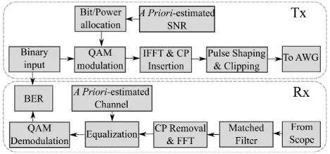
[image:3.595.68.286.51.232.2]Fig. 4. Block diagram for OFDM transmitter and receiver
bandwidth yet shown in the violet wavelength band.
3. VLC System 3.A. Optical OFDM
Multiple variants of OFDM have been proposed for VLC [15]. Conventional OFDM waveforms are both complex and bipolar, however Hermitian symmetry can be imposed on the OFDM subcarriers frame to realize real-valued OFDM waveforms, X[k] = X∗[N
FFT−k],
where NFFT is the OFDM frame size, and k is the
subcarrier index. In addition, subcarriers at X[0] and X[NFFT/2] are set to zero. DC-biased optical OFDM
(DCO-OFDM) uses a DC bias to shift most of the nega-tive real-valued OFDM samples into posinega-tive. The block diagram for OFDM is shown in Fig. 4. The generation of DCO-OFDM in this VLC experiment starts with gener-ating a real-valued OFDM waveform in MATLABR
. A pseudo-random bit sequence (PRBS) is generated and then modulated using quadrature amplitude modula-tion (QAM). Given the a priori estimated SNR, the Mk-QAM constellation size at subcarrierk and its
cor-responding realtive energy,ν2
k, are adaptively allocated
based on the probability of error target,PT
e.
The QAM symbols are loaded into orthogonal sub-carriers with sub-carrier spacing equal to the symbol du-ration. The OFDM frame size is set toNFFT=1024
sub-carriers. Smaller sizes for the OFDM frame result in less statistcal significance, larger sizes result in an increased peak-to-average power ratio (PAPR). The symbols can then be multiplexed into a serial time domain output using an inverse fast Fourier transform (IFFT). Cyclic prefixes (CPs) are inserted at the start of each OFDM frame. Adequate length of the CPs,NCP, allows for ISI
to be eliminated by the computationally-efficient single-tap equalizer. A value ofNCP = 5 is found to be
suffi-cient for the ISI to be removed at less than 0.97% loss in the spectral efficiency. Root-raised cosine (RRC) pulse shaping filter is used to achieve band limited communi-cation since it allows a trade-off control between pulse duration and bandwidth requirements [16]. OFDM time domain waveforms have high PAPR due to the coinci-dence of multiple in-phase QAM symbols in the same OFDM frame. Extreme values for the OFDM modu-lating signal are clipped to minimize the effect of non-linearity at acceptable error margins. The upper and
are used since the upper clipping due to the saturation of the micro-LED is higher than the lower clipping. The received waveform is processed with matched filters, fast Fourier transform (FFT) with CPs removal, single-tap equalizer using the a priori estimated channel, and de-modulator. Bit error rate (BER) is calculated based on the demodulated binary stream.
Before any data tranmission, the channel is first es-timated by pilots composed of multiple OFDM frames. A conventional mean estimator is used with random pi-lots that would take the nonlinearity effects into account. Details about the used estimation method can be found in [17]. An estimation of the SNR is also obtained using the same method. The received OFDM waveform,y(t), can be expressed as follows:
y(t) =h(t)∗z(x(t)) +n(t), (1)
where h(t) is the VLC system channel, n(t) is the ad-ditive white Gaussian noise (AWGN) at the receiver with a variance σ2
n, and z(.) is the nonlinear
transfor-mation of the micro-LED. For Gaussian inputs such as the real-valued OFDM waveform, the Bussgang theorem can be applied and the nonlinear transformation can be expressed as [18]:
z(x(t)) =αx(t) +d(t), (2)
given that the processes x(t) and d(t) are uncorrelated E[x(t)d(t)] = 0, where E[.] is the statistical expectation andd(t) is the distortion noise. The constantαcan be calculated as [18]:
α= E[z(x(t)).x(t)] σ2
x
. (3)
The distortion noised(t) is a non-Gaussian noise. How-ever, its representation in the frequency domain D(f) follows a Gaussian distribution with a DC mean and a varianceσ2
d [18]. Detailed analysis of the nonlinear
dis-tortion noise effect on DCO-OFDM can be found in [19]. The used arbitrary waveform generator (AWG) has 10 bits resolution for the digital-to-analog converter (DAC), and the oscilloscope used has an effective number of bits 5.5 for the analog-to-digital converter (ADC). The non-linearity effect from the amplifier is minimal at the oper-ational frequencies and at the injected power levels. The harvested optical power at the photoreceiver is well be-low the saturation level. Therefore, the micro-LED is as-sumed to be the main source of nonlinearity in the over-all system due to the relatively limited dynamic range, compared to other system components.
(b) Sub-carrier index
0 100 200 300 400 500
ν
2 k
0 0.5 1 1.5
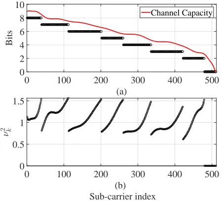
Fig. 5. (a) The bit loading and channel capacity per subcar-rier, both given in bits per subcarrier. (b) Energy loading per subcarrier.
subcarriers which require minimal additional power to be elevated into larger constellation sizes, while preserv-ing the probability of error target,PT
e. Assuming that
NFFT>64, the adaptive bit and energy loading can be
formulated in the following optimization problem:
maximize
η η=
NFFT
2 −1
X
k=1
Mk>0
log2Mk
(NFFT+NCP)(1 +β)
, (4a)
subject to BER
Mk, ν
2
kα2Ebk
No/|H(k)|2+σd2
≤PeT,
(4b)
NFFT
2 −1
X
k=1
Mk>0
ν2
k
NFFT
2 −1
= 1, (4c)
where β is the roll-off factor of the RRC filter, Ebk is
the energy per bit at subcarrierk,Nois the double-sided
power spectral density (PSD) of the noise at the receiver, |H(k)|2 is the channel gain at subcarrierk when a zero
forcing (ZF) equilzer is used,η is the spectral efficiency given in bits/s/Hz, and BER(Mk,γk) is the theoretical
BER equation ofMk-QAM at subcarrierkand SNR per
bitγk, given in non-flat channels as [21]:
BER(Mk, γk)∼=
4 log2(Mk)
1−√1 Mk
×
R X
l=1
NFFT
X
k=1
Q (2l−1)
s
3 log2(Mk)γk
2(Mk−1) !
, (5)
where Q(.) is the complementary cumulative
distribu-10
15
20
25
SNR (dB)
0
0.2
128-QAM 32-QAM
8-QAM
64-QAM 16-QAM
[image:5.595.327.557.52.234.2] [image:5.595.60.286.53.256.2]4-QAM
Fig. 6. The statistical CDF for different QAM constellation sizes experimentally achieved at a BER=2.3×10⁻³, below
the FEC target.
tion function (CCDF) for the standard normal distribu-tion, andR= min(2,√Md).
The adaptive bit and energy loading on each subcar-rier is shown in Fig. 5 along with the channel capacity limit defined by Shannon as [22]:
C= log2
1 + α
2E
bk
No/|H(k)|2+σ2d
, (6)
[image:5.595.66.297.389.532.2]It is shown that the gap between the exact loading and the capacity limit is already small, however, it can be closed when channel coding is employed. The cumula-tive distribution function (CDF) of the estimated SNR for multiple QAM constellation sizes are presented in Fig. 6. The results show the distribution of the SNR values required to achieve a BER below the forward er-ror correction (FEC) target based on the bit and energy loading algorithm.
3.B. Experimental Set-up
The experimental set-up, shown in Fig. 7, starts with a laptop connected to a Tektronix AWG (AWG70001A) that has a maximum sampling frequency of 50 GS/s with an ADC resolution of 10 bits per sample. Bipolar OFDM waveforms are generated in MATLABR
as detailed in Section 3.A and then transmitted to the AWG. The maximum peak-to-peak voltage (VPP) of the AWG is
0.5 VPP. The output of the AWG is amplified with a
broadband amplifier (SHF 100AP) that has a maximum gain of 20 dB in the bandwidth range (100 kHz–20 GHz). A 3 dB attenuator is used at the output of the amplifier to allow flexible control of the signal modulation depth, VPP. The power budget of the system is adjusted to
allow complete utilization of the micro-LED dynamic range shown in Fig. 2.
Attenuator
(a) Schematic
16 cm
11.5 cm Microscope objective lens
Newport (M-40x)
SI-PIN Photoreceiver FEMTO (HSPR-X-I-1G4-SI)
Violet Micro LED
Bi-Convex lens Thorlabs (LB4879)
Plano-Convex lens Thorlabs (LA1116)
Mirror Thorlabs (CM1-E02)
[image:6.595.60.291.51.383.2](b) Photograph
Fig. 7. The experimental set-up. (a) Schematic set-up of the experiment showing the optical system, AWG, oscilloscope, amplifier, attenuator, and Bias-tee. (b) Photograph of the optical system showing the micro-LED, optical lenses system, and the photoreceiver.
for the DC bias results in high zero-level clipping of the OFDM waveform which degrades the SNR. High values for the DC bias results in optical power satura-tion at the micro-LED which also degrades the SNR. After extensive experiments, the DC bias is set to IDC = 30 mA corresponding to a measured DC
volt-age of VDC = 5.23 V. This value allows the OFDM
bipolar signal to swing in the linear region of the L-V characteristic of the micro-LED. The biased signal is then fed to the micro-LED via a high speed probe. An optical plano-convex lens (Thorlabs LA1116) is used to collimate most of the light into a dielectric mirror (Thorlabs CM1-E02) with higher than 97% reflectance in the desired wavelength region. The reflected light is then focused onto the photoreceiver by a bi-convex lens (Thorlabs LB4879) followed by a microscopic objective lens (NewPort M-40x) with a numerical aperture (NA) of 0.65. A silicon positive-intrinsic-negative (PIN) pho-toreceiver is used (Femto HSPR-X-I-1G4-SI) with a 3 dB bandwidth of 1.4 GHz and a responsivity of 0.135 A/W around 400 nm.
-5 -4 -3 -2
Recieved optical power (dBm)
3 3.5 4 4.5
Data rate (Gb/s)
0 0.5 1 1.5 2 2.5 3
BER
Data rate BER
Theoritcal BER
Fig. 8. Experimentally obtained results and theoretical
bounds of data rate and BER versus different dimming levels at a modulation depth ofVPP= 2.36 V. The values for the received optical power correspond to DC bias values ranging from 10 mA to 40 mA.
4. Results and Discussion
The VLC data transmission experiment was only con-ducted on the inner pixels due to their higher E-O band-width compared to the outer pixels. The sampling fre-quency of the AWG is set to 29 GS/s with an over sam-pling factor of 8 samples per symbol, which results in a single-sided modulation bandwidth of 1.81 GHz. The subcarriers are equally spaced within the Nyquist rate of the modulation signal with a subcarrier spacing of 3.54 MHz. The high-speed equipment used in the mea-surements allowed for the overall system bandwidth to be limited by the bandwidth of the micro-LED. Figure 8 shows the data rates, and the corresponding theoretical lower bounds and experimentally obtained values for the BERs at different dimming levels. The theoretical lower bounds for the BER estimations are calculated based on the experimentally estimated SNR as described in (5) and they are shown to be close to the experimen-tal results. The data rates starts with 3.46 Gb/s at a received optical power, Popt =-4.94 dBm, which
corre-sponds to a DC bias ofVDC=4.16 V and a DC current
of IDC =10 mA. The data rate increases, but starts to
saturate as the DC bias increases until it reaches a maxi-mum of 4.91 Gb/s atPopt=-2.29 dBm corresponding to
VDC=5.21 V andIDC=35 mA. The data rate starts to
decrease as the DC bias increases beyond 35 mA. This re-sult is expected due to the increased clipping distortion caused by the optical power saturation shown in Fig. 2. The achieved BER for all the studied cases in this test is well below the 3.8×10⁻³FEC threshold. The optimized
DC bias was selected for the rest of the measurements as VDC =5.11 V and IDC =30 mA, since the system
performance for a larger swing of the peak-to-peak mod-ulation signal starts to degrade at IDC =35 mA. The
[image:6.595.328.551.53.222.2]3 4 5 6 7
Data rate (Gb/s)
10-6
-3.97 dBm -3.37 dBm -2.29 dBm -2.07 dBm
4.6 4.7 4.8 4.9
2 2.5
Fig. 9. Theoretical bounds on the data rate versus BER for different dimming levels at a modulation depth of VPP=2.36 V. The values for the received optical power cor-responds to DC bias values ranging from 10 mA to 40 mA. Filled markers denote experimental results.
comparison to the experimental results. The deviation between theoretical and experimental validation point at Popt=-4.94 dBm is due to the severe clipping distortion
at DC currentIDC=10 mA.
The system performance as a function of the modula-tion signal depth,VPPis investigated. Large modulation
signal swing is expected to increase the SNR due to the increased signal power, σ2
x. Nevertheless, it incurs
addi-tional nonlinear distortion,σd2, due to the increased
clip-ping. It is shown in Fig. 10 that the SNR improves as the modulation depth increases. The nonlinear distortion is present on the first 250 MHz, however the improvement in the signal power σ2
x is more significant at higher
fre-quencies. This result is justified by the fact that signals at higher frequencies are attenuated due to the lower channel gain at these high frequencies. Therefore, these values become less affected by the nonlinearity of the device. This result shows that tolerating additional non-linearity by employing a larger signal swing can improve the communication system performance.
The experimentally optimized values for the DC bias at 30 mA and the modulation signal swing at 3.88VPP
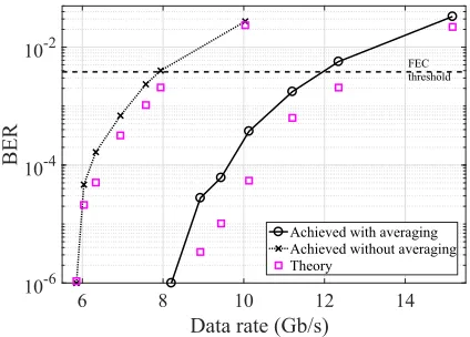
are used to investigate the system data rate performance against BER. The experimentally obtained data rates versus BERs are presented with the theoretical lower bounds for the BER performance in Fig.11. The theo-retical lower bounds are shown to be very close to the experimentally obtained results. As shown in Fig. 11, transmission data rate of 7.91 Gb/s is experimentally achieved at a BER below the FEC threshold, 3.8×10⁻³.
To guarantee reliable communications, the data rate is reduced to 7.36 Gb/s to allow for a 7% FEC overhead to be employed. This compares to 5 Gb/s for a device with similar design emitting at 450 nm [7]. To the best of the authors’ knowledge, this record is the highest for VLCs data transmission speeds using single micro-LED.
Bandwidth (GHz)
0 0.2 0.4 0.6 0.8 1 1.2 1.4 1.6 1.8
0 5
[image:7.595.67.287.49.222.2]0 0.1 0.2 0.3 20
Fig. 10. SNR versus frequency for different modulation
depths at DC bias current IDC =30 mA. The values for
the modulation signal swings corresponds to feeding the micro-LED with varying power levels from 5.85 dBm to 11.78 dBm.
6 8 10 12 14
Data rate (Gb/s)
10-6
10-4
10-2
BER
Achieved with averaging Achieved without averaging Theory
FEC threshold
Fig. 11. Data rates versus BER for the experimentally
obtained and the theoretical bounds at DC bias current
IDC =30 mA corresponding to Popt=-2.6 dBm and
modu-lation depthVPP=3.88 V.
[image:7.595.331.551.50.206.2] [image:7.595.331.543.288.440.2]100 200 300 400 500 D -5 -4.5 -4 -3.5 R 3 3.5 4
T !"#
T$ % ! "#!#
Data rate
1 2 3 4 5 6
& '() *+, -., / 0
-5 -4.5 -4 -3.5 1 2 3 4 2 5 2 7 8 9 : 4 3 ; < 9 3 3.5 4 C ; : ; > ; : 2 ?
O PJ K LM
Data rate
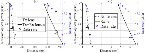
Fig. 12. Distance versus received optical power (left) and data rate (right). (a) for Study I with transmitter and re-ceiver lenses and Study II with transmitter lens only. (b) for Study III with receiver lens only and Study IV without any optics.
5. Range and Alignment Considerations
The VLC system was realized using an optical system to collect, collimate, and focus the light on the photodiode (PD). The used optical system imposes restrictions on the link alignment and transmission range. Introducing optimized optics and deploying more micro-LED pixels from the array can improve both the coverage and the range of the system. The feasibility of demonstrating long transmission distances was demonstrated at a free-space distance of 10 m and a data rate of 1.1 Gb/s in [24]. This was achieved using an avalanche photodiode (APD) with an integrated concentrator, and a micro-LED with an optical power of 4.5 mW, which is 1.96 times higher than the optical power of the micro-LED pixel used in this work.
The obtained data rates and BERs for different re-ceived optical power presented in Fig. 8 enable us to investigate the system performance against the trans-mission range based on the widely accepted line-of-sight (LoS) optical wireless communication (OWC) propaga-tion models [25]. The methodology is to compute the distances which result in the respective received optical power presented in Fig. 8, and the distances are then cross-mapped with the data rates achieved in Fig. 8. Note that the results shown in Fig. 8 are obtained at different dimming levels by varying the DC bias point which limits the operating bandwidth and the experi-mentally obtained data rates. An analysis of the sys-tem range is provided based on four studies: (I) with transmitter and receiver lenses; (II) with transmitter lens only; (III) with receiver lens only; (IV) without any optics. In all cases we assume that all array pixels are used (15 micro-LEDs) in a ganging OFDM mode. This can increase the mutual heat between the pixels and con-sequently degrades the total aggregate data rates, there-fore the results in this section can be considered as upper bounds on the system performance.
The LoS channel gain can be given as [25]:
H(0) =(m+ 1)A 2πd2 cos
m(φ)T(ψ)g(ψ) cos(ψ), (7)
wherem=−1/log2(cos(Φ1/2)) is the Lambertian order
of the optical source and Φ1/2 denotes its semi-angle;
T(ψ) represents the gain of the optical filter used at the receiver; andg(ψ) represents the gain of the optical con-centrator, given as [25]:
g(ψ) =
( n2
sin2(Ψ
fov), 0≤ψ≤Ψfov
0, ψ >Ψfov
, (8)
where n is the refractive index of the optical concen-trator used at the APD. The optical power after the transmitter lens can be given as [26]:
PoptR,lens=
(mLED+ 1)Dlens2
8d′2 TlensP T,LED
opt , (9)
where mLED denotes the Lambertian order of the
micro-LED,Dlensis the lens diameter,Tlensis the
trans-mittance of the lens, and d′ is the distance between the micro-LED and the transmitter lens. The existence of the transmitter lens affect the micro-LED beam diver-gence. The half power semi-angle Φlens
1/2 can be given as
[26]:
Φlens1/2 =
Ds
2d′, (10)
whereDs is the diameter of the micro-LED. The
trans-mitter lens used in this investigation is aspheric con-denser lens (Thorlabs ACL7560U-A) with a diameter of Dlens= 75 mm, and a focal length of lensf = 60 mm.
A commercially available compound parabolic concen-trator (CPC) is assumed to be in front of the APD. The field-of-view (FOV) of the concentrator is 25◦, with a refractive index of n = 1.5. We assume the use of a high speed commercially available APD at the receiver (Thorlabs APD210) instead of the used positive-intrinsic-negative (PIN) receiver (Femto HSPR-X-I-1G4-SI). The APD diameter is 0.5 mm and the modulation bandwidth is 1.6 GHz. The APD improves the sensitivity of the re-ceiver, therefore an APD conversion gain factor is intro-duced to allow a fair comparison between the experimen-tally obtained results using the PIN and the numerical results using the APD photoreceivers:
ΛAPD= G
APD
GPIN, (11)
where GAPD and GPIN are the conversion gains of the
APD and PIN photoreceivers given in V/W, respectively. Using Equations (7) to (11), the received optical power at the APD can be given as:
PoptRx,APD=
(mlens+ 1)A
2πd2 cos
mlens(φ)
×
T(ψ)g(ψ) cos(ψ)ΛAPDPoptR,lens, (12)
wheremlensis the Lambertian order of the lens based on
[image:8.595.54.296.54.143.2]-5.14 -5.14 -5.14 -5.14 -5.12 -5.12 -5.12 -5.12 -5.12 -5.12 -5.1 -5.1 -5.1 -5.1 -5.1 -5.08 -5.08 -5.08 -5.08 -5.06 -5.06
-5 0 5
-5 0 5
V WX Y Z V WX Y[ -5.14 -5.12 -5.1 V WX\Z -6.2 -6.2 -6.2 -6.2 -6 -6 -6 -6 -5.8 -5.8 -5.8 -5.8 -5.8 -5.8 -5.6 -5.6 -5.6 -5.6 -5.6 -5.4 -5.4 -5.4 -5.4 -5.2 -5.2 -5.2
-5 0 5
-5 0 5 V[X W V[ -5.5 -5.07 -5.07 -5.07 -5.07 -5.06 -5.06 -5.06 -5.06 -5.05 -5.05 -5.05 -5.05 -5.05 -5.04 -5.04 -5.04 -5.04 -5.04 -5.03 -5.03 -5.03 -5.03 -5.02 -5.02 -5.02 -5.01 -5.01
-5 0 5
-5 0 5 -5.1 ]^_ `a ]^_ `b -5.04 -5.02 -6 -6 -6 -6 -5.9 -5.9 -5.9 -5.9 -5.8 -5.8 -5.8 -5.8 -5.7 -5.7 -5.7 -5.7 -5.7 -5.6 -5.6 -5.6 -5.6 -5.6 -5.5 -5.5 -5.5 -5.5 -5.4 -5.4 -5.4 -5.3 -5.3 -5.3 -5.2
-5 0 5
-5 0 5 cd ef cd cgeh cged -5.4 -5.2
(d) ) (h)
Fig. 13. Received optical power distribution in dBm as a function of vertical-horizontal displacements. (a) Study I at a distance of 369 cm; (b) Study I at a distance of 525 cm; (c) Study II at a distance of 104 cm; (d) Study II at a distance of 147 cm; (e) Study III at a distance of 4.7 cm;(f) Study III at a distance of 6.6 cm;(g) Study IV at a distance of 1.3 cm; (h) Study IV at a distance of 1.9 cm.
The LoS propagation model is used to compute the transmission ranges that can achieve certain values for the received optical power between -5 dBm and -2 dBm. These values for the received optical power were demon-strated experimentally to achieve data rates between 3.46 Gb/s and 4.91 Gb/s using the experimentally real-ized VLC system. An upper bound on the data rates can be estimated by cross-mapping the computed re-ceived power at each distance, with the experimentally obtained data rates provided in Fig.8. The distance ver-sus received optical power and data rate for Studies I and II and studies III and IV are shown in Fig. 12, re-spectively. The largest distances can be achieved us-ing transmitter and receiver optics. Specifically, it was found that at 3.69 m distance a data rate of 4.91 Gb/s can be achieved, and at 5.25 m distance the data rates reduces to 3.46 Gb/s. As expected, the transmitter lens is shown to boost the range more than the receiver con-centrator lens. At a data rate of 4.91 Gb/s, the maxi-mum distance is 1.04 m and 4.7 cm for studies II and III, respectively. At a data rate of 3.46 Gb/s, the max-imum distance is 1.47 m and 6.6 cm for studies II and III, respectively. The transmission ranges that can be supported at data rates above 3.46 Gb/s are less than 2 cm when optics are not used.
The received optical power distribution is investigated as a function of the receiver’s vertical-horizontal mis-alignments for the four considered studies, as shown in Figure 13. The results are presented for the received op-tical power values that allow a maximum of -2 dBm and a minimum of -5 dBm, corresponding to data rates of 4.91 Gb/s and 3.46 Gb/s, respectively. The transmission range and the system robustness against misalignments are both improved when optics are used for both
front-end components in Study I, which makes this scenario suitable for high-speed point to point applications. The transmitter lens in Study II improves the transmission range but reduces the system robustness against mis-alignments. The receiver lens in Study III is reducing the performance degradation caused by misalignment at the expense of reducing the system range. The transmis-sion range and the system robustness against misalign-ments are both degraded in Study IV. However, Studies III and IV are suitable for board to board communica-tion links, where wired links are not possible because of the rotational requirements between the boards for example.
6. Conclusion
A novel violet micro-LED array with two sets of inner and outer pixels is reported in this paper. The inner pixels allow very high current densities due to the small active area, enabling E-O bandwidth up to 655 MHz at an optical output power of 2.3 mW.
over-The numerical investigation of the range and align-ment highlight the role of optimized optics in increasing the transmission distance and improving system robust-ness.
Acknowledgement
The authors gratefully acknowledge the financial support from EPSRC through the programme grant “UP-VLC” (EP/K00042X/1). M. S. Islim acknowledges the partial
financial support from EPSRC (EP/M506515/1).
References
[1] Cisco Visual Networking Index, “The Zettabyte era: trends and analysis,” White Paper, Cisco (2015),http: //www.cisco.com/c/en/us/solutions/collateral/ service-provider/visual-networking-index-vni/ VNI_Hyperconnectivity_WP.pdf.
[2] Y. Zhou, J. Zhao, M. Zhang, J. Shi and N. Chi, “2.32 Gbit/s phosphorescent white LED visible light com-munication aided by two-staged linear software
equal-izer,” in 10th International Symposium on
Communi-cation Systems, Networks and Digital Signal Processing (CSNDSP), (IEEE, 2016), pp. 1–4.
[3] J. Herrnsdorf, J.J.D. McKendry, E. Xie, M.J. Strain, E. Gu, I.M. Watson, and M.D. Dawson, ”Gallium Ni-tride structured illumination light sources,” in Light, En-ergy and the Environment conference, (Optical Society of America, 2016), paper SSM2C.1.
[4] J.J.D. McKendry, R.P. Green, A.E. Kelly, Z. Gong, B. Guilhabert, D. Massoubre, E. Gu, M.D. Dawson, “High-speed visible light communications using individ-ual pixels in a Micro light-emitting diode array,” IEEE Photon. Technol. Lett.22, 1346–1348 (2010).
[5] P.P. Maaskant, H. Shams, M. Akhter, W. Henry,
M.J. Kappers, D. Zhu, C.J. Humphreys, and
B. Corbett, “High-speed substrate-emitting Micro-light-emitting diodes for applications requiring high radiance,” Appl. Phys. Expr.6, 022102 (2013).
[6] D. Tsonev, H. Chun, S. Rajbhandari, J.J.D. McKendry, S. Videv, E. Gu, M. Haji, S. Watson, A.E. Kelly, G. Faulkner, M.D. Dawson, H. Haas, and D. O’Brien, “A 3-Gb/s single-LED OFDM-based wireless VLC link
using a Gallium NitrideµLED,” IEEE Photon. Technol.
Lett.26, 637–640 (2014).
[7] R. Ferreira, E. Xie, J. McKendry, S. Rajbhandari, H. Chun, G. Faulkner, S. Watson, A.E. Kelly, E. Gu, R. Penty, I. White, D. O’Brien, and M.D. Dawson, “High bandwidth GaN-based micro-LEDs for multi-Gbps visi-ble light communications,” IEEE Photon. Technol. Lett.,
28, 2023–2026, (2016).
[8] C.J. Humphreys, “Solid-state lighting,” MRS bulletin, Cambridge Univ Press33, 459–470 (2008).
[9] A. Zukauskas, R. Vaicekauskas and M.S. Shur, “Colour-rendition properties of solid-state lamps,” J. Appl. Phys. D43, 354006 (2010).
[10] J.M. Phillips, M.E. Coltrin, M.H. Crawford, A.J. Fis-cher, M.R. Krames, R. Mueller-Mach, G.O. Mueller,
(2007).
[11] Q. Dai, Q. Shan, H. Lam, L. Hao, Y. Lin and Z. Cui, “Circadian-effect engineering of solid-state lighting spec-tra for beneficial and tunable lighting,” Opt. Exp. 24,
20049-20058 (2016).
[12] Z. Gong, Y.F. Zhang, P. Kelm, I.M. Watson, E. Gu, and M.D. Dawson, “InGaN micro-pixellated light-emitting diodes with nano-textured surfaces and modified emis-sion profiles,” Appl. Phys. A103, 389-393 (2011).
[13] D.J.F. Barros, S.K. Wilson and J.M. Kahn, “Compar-ison of orthogonal frequency-division multiplexing and pulse-amplitude modulation in indoor optical wireless
links,” IEEE Trans. Commun.60, 153–163 (2012).
[14] J. McKendry, D. Tsonev, R. Ferreira, S. Videv, A. Grif-fiths, S. Watson, E. Gu, A. Kelly, H. Haas, and M. Daw-son, “Gb/s single-LED OFDM-based VLC using violet
and UV Gallium Nitride µLEDs,” in IEEE Summer
Topicals Meeting Series (SUM), (IEEE, 2015), paper TuD4.3.
[15] M.S. Islim, and H. Haas, “Modulation techniques for Li–
Fi,” ZTE COMMUNICATIONS14, 29–40 (2016).
[16] D. Tsonev, S. Sinanovic, and H. Haas, “Complete modelling of nonlinear distortion in OFDM-based opti-cal wireless communication,” J. Lightwave Technol.31,
3064–3076 (2013).
[17] D. Tsonev, S. Videv, and H. Haas, “Unlocking spectral efficiency in intensity modulation and direct detection
systems,” IEEE J. Sel. Areas Commun. 33, 1758–1770
(2015).
[18] P. Banelli and S. Cacopardi, “Theoretical analysis and performance of OFDM signals in nonlinear AWGN
chan-nels,” IEEE Trans. Commun.48, 430–441 (2000).
[19] S. Dimitrov and H. Haas, “Information rate of OFDM-based optical wireless communication systems with non-linear distortion,” J. Lightwave Technol. 31, 918–929
(2013).
[20] H.E. Levin,“A complete and optimal data allocation method for practical discrete multitone systems,” in Pro-ceedings of IEEE Global Telecommunications Conference
(IEEE, 2001), pp. 369–374.
[21] F. Xiong,Digital Modulation Techniques, (Artech House Publishers, 2006), 2nd ed.
[22] CE. Shannon, “A mathematical theory of
communi-cation,” Bell System Technical Journal 27, 379–423
(1948).
[23] L. Peng, S. Haese and M. H`elard, “Optimized discrete multitone communication over polymer optical fiber,”
IEEE J. Opt. Commun. Netw.5, 1313–1327 (2013).
[24] J. Jiang, Y. Huo, F. Jin, P. Zhang, Z. Wang, Z. Xu, H. Haas, and L. Hanzo, “Video streaming in the mul-tiuser indoor visible light downlink,” IEEE Access 3,
2959–2986 (2015).
[25] J. M. Kahn and J. R. Barry, “Wireless Infrared Commu-nications,” Proc. IEEE85, 265–298 (1997).