2017 INTERNATIONAL CONFERENCE ON MICROELECTRONIC TEST STRUCTURES, MARCH 28-30, GRENOBLE, FRANCE
7.3
978-1-4673-XXXX-X/17 $XX.XX © 2017 IEEE
Test structures for optimizing polymer electrolyte
performance in a microfabricated electrochemical
oxygen sensor
J.R.K. Marland1, C. Dunare1, A. Tsiamis1, E. González-Fernández2, E.O. Blair1, S. Smith1, J.G. Terry1, A.F. Murray1, A.J. Walton1
1School of Engineering, University of Edinburgh,Alexander Crum Brown Road, Edinburgh, EH9 3FF, UK 2School of Chemistry, University of Edinburgh, Joseph Black Building, David Brewster Road, Edinburgh, EH9 3FJ, UK
Email: [email protected]
Abstract—Test structures were produced for optimizing the design and fabrication of a patterned solid polymer electrolyte in an electrochemical oxygen sensor. Measurements showed that choice of photoresist developer and the underlying insulator material affected durability of the polymer structures. Test electrodes covered by the polymer were effective at supporting electrochemical oxygen detection.
I. INTRODUCTION
A Clark electrode with a membrane covered cavity containing a liquid electrolyte is a well-established oxygen sensor for biochemical measurement. However, this architecture does not lend itself to miniaturization using standard microsystem technologies. An alternative approach is to use the solid electrolyte Nafion. This is a polymer with ionic properties that contains hydrated channels capable of conducting protons [1]. It has been reported as a suitable electrolyte membrane in electrochemical sensors that detect dissolved oxygen [2]-[4], however little has been reported about microfabrication of Nafion membranes. In order to explore this issue quantitatively, we report the use of test structures to characterize and optimize the design and patterning of Nafion. A set of test electrodes was also fabricated to demonstrate the ability of a microfabricated Nafion membrane to support electrochemical reactions. The results from these test structures will be used to inform the implementation of a future miniaturized oxygen sensor for medical implantation.
II. NAFION ADHESION AND DURABILITY TEST STRUCTURES
A. Design
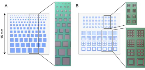
Two layouts containing simple geometric test structures were designed to optimize the fabrication process and investigate the effects of layout parameters and underlying materials on Nafion adhesion and durability under simulated conditions of use. Layout A is comprised of Nafion squares with widths ranging from 200µm to 1600µm (Fig. 1A). These were designed to test the effect of varying the area of the Nafion structure on its performance. Layout B is comprised of two series of structures in which the total area of Nafion in each was held constant, at either 1.0 mm2 or 0.2 mm2, and split into sequentially finer grids with smaller dimensions (Fig. 1B).
The reduction in dimensions was achieved using smaller line widths and decreasing spacing between divisions. The aim of the Layout B structures was to distinguish between effects of area and linear dimension on any differences in Nafion performance that might be shown by the squares in Layout A. Both Layouts were designed within 15 mm square blocks, and a total of 24 blocks (12 of each Layout) were distributed in an alternating pattern across the surface of a 4” (100 mm) silicon wafer.
B. Fabrication
[image:1.595.311.550.258.374.2]To fabricate the test structures, materials that would potentially be used for either the sensor electrodes (platinum), or the top dielectric layer, were deposited on silicon wafers. The top dielectric was plasma enhanced chemical vapor deposited (PECVD) with low-frequency/high-frequency silicon nitride, referred to here as LFSIN/HFSIN, or silicon dioxide, denoted as LFSIO/HFSIO. The wafers were treated with a silane based adhesion promoter then spin coated with a Nafion solution that was dried in air and thermally annealed to improve solvent resistance. Wafers were then coated in SPR350 photoresist, and the test structure patterns transferred into photoresist by photolithography (Karl Suss MA8). The photoresist was developed using either MF-26A or AZ726 photoresist developer in order to compare their effects on test structure performance. Nafion was patterned by reactive ion etching (RIE) in an O2/CF4 plasma. Photoresist was stripped
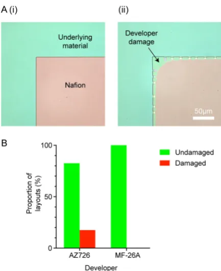
off the wafer using an acetone wet stripping process prior to testing. Profilometry measurements of Nafion features gave a mean thickness of 0.50 ± 0.02 µm across the fabricated wafers. Optical inspection of the test structures on wafers processed using AZ726 photoresist developer indicated that some displayed damage to their edges suggesting delamination, while wafers processed using MF-26A developer were all intact and undamaged (Fig. 2). MF-26A and AZ726 developers are both based on an alkaline aqueous solution of tetramethylammonium hydroxide (TMAH). However, as they have an identical TMAH concentration of 0.26N, it is likely that different proprietary additives such as surfactants present in the developers may be responsible for their differing compatibility profiles.
III. ADHESION MEASUREMENTS
Nafion adhesion strength on the different materials was measured using a scratch tester (Keysight Nanoindenter G220). This tool draws a sharp tip across the surface of the layer under test with a ramping increase in downward force. The tip force when the layer fails is defined as the critical load, and its magnitude scales with adhesion strength between the layer under test and the underlying material [5]. Two selected locations on each wafer were measured, and for each test location an array of 10 scratches was performed.
Optical inspection of the scratches made in Nafion showed that it underwent initial plastic deformation, followed by buckling and failure of the layer as it became detached from the
wafer (Fig. 3A(i)). Profilometry was used to inspect the scratch location before and after testing in order to identify the exact failure point, and showed a similar pattern (Fig. 3A(ii)). Comparison of the scratch test results showed no significant differences in Nafion mean critical load between any conditions (Fig. 3B). This suggests that there were no differences between Nafion adhesion on any of the tested insulation layers, or on the conductive platinum layer.
IV. DURABILITY MEASUREMENTS
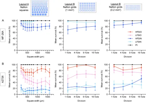
To investigate whether any of the tested design parameters affected Nafion durability, wafers carrying test structures were immersed in an aqueous phosphate buffered saline (PBS) solution, formulated to mimic the ionic composition of the body. Wafers were left in the solution for 6 weeks to simulate typical duration of use for the future oxygen sensor. As a measure of durability, survival of the test structures was evaluated by comparison of optical microscope images before and after immersion. A total of 12 instances of each test structure Layout were tested for each combination of developer and underlying material. Structures were classified as having survived if they were undamaged at the end of the test, or failed if they were damaged or absent (Fig. 4).
[image:2.595.55.272.52.318.2]There was a clear effect of the developer used during processing, with wafers processed using MF-26A showing higher overall survival (Fig. 5A), compared to those processed using AZ726 (Fig. 5B). The difference in failure rate
Fig. 2. Photoresist developer damage to Nafion test structures. A: Example images showing corners of patterned Nafion test structures that were visibly either (i) undamaged, or (ii) damaged by photoresist developer during processing. B: Proportion of layouts damaged by different developers; n = 120 layouts from 5 wafers for each developer.
[image:2.595.319.531.55.338.2]corresponds with the finding that damage to the Nafion edges (shown in Fig. 2) was limited to wafers processed in AZ726. This suggests that the two effects may be linked, with damage during processing causing partial edge delamination that ultimately leads to failure of the structure during testing. Together, these results indicate that MF-26A is optimal for Nafion processing in this application.
The underlying material also had a marked effect on structure survival. The poorest survival was observed on wafers with PECVD silicon nitride surfaces. In contrast, structures fabricated on PECVD silicon dioxide surfaces showed
intermediate survival on the wafers processed with AZ726, and near complete survival on wafers processed with MF-26A. This greater survival of structures on silicon dioxide may be attributable to the silane based adhesion promoter used during fabrication. It relies on a condensation reaction between an alkoxysilyl group in the adhesion promoter, and a hydroxyl (-OH) group found on the wafer surface of hydrated silicon dioxide. Since few hydroxyl groups will be present on the silicon nitride, the adhesion promoter would be expected to perform less efficiently on this surface. The optimal PECVD deposition frequency appeared to be material specific, with better survival obtained for silicon nitride using low frequency deposition, and for silicon dioxide using high frequency deposition. Together these results show that use of PECVD high frequency silicon dioxide as an upper insulating layer is optimal for Nafion membrane durability in a sensor. Interestingly, across all the materials tested, the best survival was obtained on platinum. This indicates that durability of the membrane will not be impaired by the presence of underlying platinum electrodes.
[image:3.595.90.236.60.130.2]It is notable that these survival results do not correlate with the adhesion measurements from scratch testing (Fig. 3). This suggests that the scratch test critical load of Nafion is not usable as an indicator of its durability in PBS.
Fig. 4. Example images showing survival and failure of Nafion test structures following immersion in PBS. Outlines of the structures remaining after failure are visible due to over-etching of the wafer material outside the Nafion structure during fabrication.
[image:3.595.62.531.349.681.2]Nafion is known to swell in aqueous environments [1], which is likely to generate compressive stress within the layer that could lead to its failure. Such an effect is predicted to be strongest in larger structures with a greater area over which stress could build up. In keeping with this possibility, inspection of the structure survival data from Layout A (Nafion squares) shows a trend towards increased survival of smaller sizes, with the best survival typically obtained at the smallest 200µm square width. This suggests that minimizing Nafion membrane size may improve durability. In the Layout B (Nafion grids) data there were no clear trends in survival when the structure internal dimensions were decreased, in either the large (1mm2) or small (0.2mm2) designs. It is possible that these structures were too large for the size effect detected in Layout A to be evident. Either finer division (to reduce dimensions) or further reduction in total area may be necessary to allow the effects of layout parameters to be effectively explored using these structures.
V. TEST ELECTRODES
A. Design
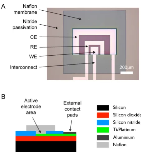
To function as an oxygen sensor electrolyte, the fabricated Nafion membrane must be both oxygen permeable and effectively support the electrochemical reduction of oxygen to water. To investigate these aspects of Nafion performance, a device containing test electrodes at which oxygen reduction could occur was designed and fabricated (Fig. 6A). The device was designed as a three-electrode electrochemical cell, with a 125µm wide square platinum working electrode (WE) at which the reaction of interest occurs. This is surrounded by an ~8x larger area platinum counter electrode (CE) to supply the
necessary current to support the WE reaction. An additional electrode area for future use as an internal reference electrode (RE) was included on the device between the CE and WE, but not used in this study and left disconnected. Instead, an external commercial Ag/AgCl RE was used for all electrochemical measurements.
B. Fabrication
[image:4.595.352.507.59.437.2]The test electrodes were fabricated on thermally oxidized silicon wafers. Metal electrode surfaces and interconnect were formed from a 50 nm layer of platinum (with an underlying 10 nm titanium adhesion layer) deposited by e-bean evaporation, and patterned by lift-off processing. Aluminum was sputtered onto the wafer and patterned to form contact pads. Above the metal layer, PECVD silicon nitride was deposited to insulate the interconnect, and patterned using RIE to produce windows permitting external access to the electrodes and contact pads. The electrodes were then either
Fig. 7. Chronoamperometry of test electrodes in aqueous solutions saturated with air or purged with nitrogen. A: Typical chronoamperograms from a Nafion coated device. B: Steady state currents from bare or Nafion covered electrodes in solutions saturated with air of purged of oxygen with N2.
Currents were averaged over 15-20 sec after the potential step to -0.7V, n = 3 devices each condition, error bars represent standard error of the mean.
[image:4.595.50.277.64.314.2]
left bare, or covered in a 1000µm wide square of Nafion deposited and patterned as before, using MF-26A to develop the photoresist (Fig. 6B). Finally, the wafer was diced to enable each die to be tested separately.
C. Electrochemical testing
Nafion covered electrodes were tested in PBS, with the Nafion itself acting as the electrolyte, while the bare electrodes were bathed in 0.1M KCl as a supporting electrolyte. The solutions were either saturated with air, or purged of oxygen using N2, and the membrane and electrodes were tested by chronoamperometry over 20 sec using a WE potential step (vs. Ag/AgCl) from +0.2 V (no oxygen reaction) to –0.7 V (oxygen reduction). This gave the expected profile of an initial transient current, followed by an approach to steady state (Fig. 7A). To calculate a figure for comparison between conditions, the steady state WE current was averaged over 5 sec, starting from 15 sec after the potential step.
Chronoamperometry recordings in air saturated solutions showed that presence of the Nafion membrane lowered the steady-state currents recorded at the WE by 23%, but did not eliminate them (Fig. 7B). This indicates that the annealed and patterned Nafion membrane covering the test electrodes is both permeable to oxygen, and capable of effectively supporting its electrochemical reduction. Interestingly, it has been shown by others that deposition of Nafion onto a platinum electrode causes 15-20% of the surface area to be blocked for electrochemical reactions [6], likely because only sections in contact with the hydrated Nafion nanochannels will be active. This effect may explain the decreased current we observed.
In order to confirm that the test electrodes were selectively detecting oxygen, and explore the utility of the Nafion/test electrode system as a sensor, the same measurements were repeated in solutions purged of oxygen by bubbling with N2. Significantly lower currents were recorded from both the bare and Nafion covered test electrodes in N2 purged solutions (Fig. 7B). This indicates that the system is selectively reporting the electrochemical reactions of oxygen at the electrodes surfaces, and that Nafion shows promise as a solid electrolyte layer for an oxygen sensor.
VI. CONCLUSIONS
Test structures for assessing the performance of a Nafion solid electrolyte membrane were designed and fabricated. These structures provided quantitative information to support optimization of the Nafion design and patterning process, as well as evaluation of its performance parameters.
Specifically, we found that use of AZ726 photoresist developer during processing led to damage of the Nafion structures, which correlated with impaired durability under simulated conditions of use. In contrast, MF-26A developer did not cause damage and was associated with higher durability, so
is therefore optimal for Nafion processing. The surface that allowed greatest Nafion durability was PECVD silicon dioxide, indicating that this material should be used as a top passivation layer in a sensor. In addition, the excellent durability obtained on Pt suggests Nafion will not be adversely affected by the presence of underlying electrodes. The functional differences in durability with underlying material were not matched by changes in scratch test critical load. This suggests that scratch tests cannot be used as an indication of lifetime in PBS. Finally, the test structures also suggested that minimizing the size of a Nafion membrane may improve its durability, and further investigation with smaller test structures than those described here would allow this result to be confirmed.
Using a set of test electrodes covered with a patterned Nafion membrane, the Nafion was shown to be oxygen permeable and support the electrochemical reduction of oxygen at an electrode surface. This indicates that Nafion can act as an effective electrolyte, and provides proof-of-concept that it would be suitable for use in a miniaturized solid-state implantable oxygen sensor in biomedical applications.
ACKNOWLEDGMENTS
This work was funded by the UK Engineering and Physical Sciences Research Council, through the IMPACT programme grant (EP/K034510/1), with additional studentship support from Scottish Funding Council and the Centre for Sensor and Imaging Systems.
All data presented in this paper can be accessed at: http://hdl.handle.net/10283/2339
REFERENCES
[1] K. A. Mauritz and R. B. Moore, “State of Understanding of Nafion,” Chem. Rev., vol. 104, no. 10, pp. 4535–4586, Oct. 2004. [2] G. W. McLaughlin, K. Braden, and B. Franc, “Microfabricated
solid-state dissolved oxygen sensor,” Sensors and Actuators B: Chemical, vol. 83, no. 1, pp. 138–148, 2002.
[3] P. Wang, Y. Liu, H. D. Abruña, J. A. Spector, and W. L. Olbricht, “Micromachined dissolved oxygen sensor based on solid polymer electrolyte,” Sensors and Actuators B: Chemical, vol. 153, no. 1, pp. 145–151, 2011.
[4] W. P. Chan, M. Narducci, Y. Gao, M.-Y. Cheng, J. H. Cheong, A. K. George, D. D. Cheam, S. C. Leong, M. R. B. Damalerio, R. Lim, M.-L. Tsai, A. R. A. Rahman, M. K. Park, Z. H. Kong, R. J. Prashanth, and M. Je, “A Monolithically Integrated Pressure/Oxygen/Temperature Sensing SoC for Multimodality Intracranial Neuromonitoring,” IEEE J. Solid-State Circuits, vol. 49, no. 11, pp. 2449–2461, Nov. 2014.
[5] J. Tomastik and R. Ctvrtlik, “Nanoscratch test — A tool for evaluation of cohesive and adhesive properties of thin films and coatings,” EPJ Web of Conferences, vol. 48, p. 00027, May 2013. [6] S. K. Zecevic, “Kinetics of O2 Reduction on a Pt Electrode Covered