Rochester Institute of Technology
RIT Scholar Works
Theses
Thesis/Dissertation Collections
10-22-2001
Study of Tantalum nitride diffusion barrier films for
coppper interconnect technology
Deepa Gazula
Follow this and additional works at:
http://scholarworks.rit.edu/theses
This Thesis is brought to you for free and open access by the Thesis/Dissertation Collections at RIT Scholar Works. It has been accepted for inclusion
in Theses by an authorized administrator of RIT Scholar Works. For more information, please contact
Recommended Citation
Study
of
Tantalum Nitride Diffusion Barrier Films for
Copper Interconnect
Technology
By
Study of Tantalum Nitride Diffusion Barrier Films for Copper
Interconnect Technology
by
Deepa Gazula
I, Deepa Gazula, hereby grant perrmsslOn to the Wallace Memorial Library of the
Rochester Institute of Technology to reproduce this document in whole or in part
provided that any reproduction will not be for commercial use or profit.
Study of Tantalum Nitride Diffusion Barrier Films for Copper
Interconnect Technology
by
Deepa Gazula
A thesis submitted in partial fulfillment of the requirements for the degree of
Master of Science
in Material Science and Engineering at the Rochester Institute of Technology
Approved by
Dr.Thomas Blanton
Scientist,
Eastman Kodak Laboratories,
Rochester, NY
Dr. Andreas Langner
Department of Chemistry
&
Materials
Science and Engineering
Rochester Institute of Technology,
Rochester, NY
Dr. Santosh K.Kurinec, Advisor
Department of Microelectronics Engineering
&
Materials Science and Engineering
Rochester Institute of Technology,
Rochester, NY
Dr. Vern Lindberg
Department of Physics
&
Materials Science
and Engineering
Rochester Institute of Technology,
Rochester, NY
TABLE
OF
CONTENTS
I. LIST OF FIGURES jj
II. LIST OFTABLES ...viii
III. ACKNOWLEDGEMENTS ... ... ...ix
IV. ABSTRACT
ZZZZZZZZZZZZZZZZZZZ.
x1.1 INTRODUCTION 1
1.2 ISSUES IN METALLIZATION
ZZZZZZZZZZZZZZZZZZ..
21.2.1 Electromigration 2
1.2.2 RC
Delay
41.3 NEED FOR A NEWMETALLIZATION 5
1.4 COPPERMETALLIZATION 8
1.4.1 DisadvantagesofCopper 9
1.4.2
Patterning
ofCopper 1 11.4.2.1 Wet etching 11
1.4.2.2 Plasma etching 11
1.4.3 Changes in Process
Technology
with copper metallization 121.5 DIFFUSION BARRIERS 13
1.6 BARRIER MATERIALS 15
1.6.1 Tantalum 15
1.6.2 Tantalum Nitrides 16
1.6.3 Tantalum-Silicon-Nitride 17
1.6.4 Tungsten Nitrides 17
1.7 DAMASCENE PROCESSING 18
1.8 CHEMICAL MECHANICAL PLANARIZATION
(CMP)
191.8.1 CMPofCopper 20
1.9 DEPOSITION OF COPPER 20
1.9.1 PVDofCopper 21
1.9.2 CVDofCopper 21
1.9.3 Electroless
Plating
ofCopper 231.9.4 Electrolytic
Plating
241.10 ANALYSIS TECHNIQUES TO TEST BARRIER STABILITY 25
1.11 CONCLUSION 25
2.1 FUNDAMENTALS OF SPUTTERING 26
2.1.1 D.C. Magnetron
Sputtering
272.1.2 R.F. Magnetron
Sputtering
272.2 HYSTERESISBEHAVIORDURING SPUTTERING 28
2.3 DEPOSITION OFTANTALUMNITRIDE FILMS 29
2.4 IONTECH CYCLONE CYLINDRICALMAGNETRONSYSTEM 29
2.4.1 Experimental details 31
2.5 X-RAYDIFFRACTION TECHNIQUE 32
2.6 RESULTS 33
2.7 DISCUSSION 36
2.7.1 Hysteresis Behavior 36
2.7.2 Effectof
N2
content onresistivityandcrystalstructure 362.8 FRACTIONALFACTORIAL DESIGN: 41
2.8.1 Theanalysis ofvariance
(ANOVA)
technique 412.8.2 RESULTS ANDDISCUSSION 47
2.9 PULSED DCSPUTTERINGOFTANTALUMNITRIDE FILMS 48
3.1 BACKGROUND 51
3.2 EXPERIMENTAL PROCEDURE 51
3.3 RUTHERFORDBACKSCATTERINGANALYSIS
(RBS)
523.4 SCANNING ELECTRONMICROSCOPY
(SEM)
533.5 TRANSMISSION ELECTRONMICROSCOPY
(TEM)
543.5.1 Focused Ion Beamsystem
(FIB)
553.5.2 Procedureforpreparation of sampleforTEM 56
3.6 RESULTS ANDDISCUSSION 56
3.6.1 Optimizationofdepositionparameters 56
3.6.2
X-Ray
Diffraction Analysis 583.6.3 TEMandSEM Analysis: 64
3.6.4 Effectofannealingonresistivityand crystal phases 67
3.7 STRESSES IN FILMS 70
3.7.1 Stress Measurement 72
3.8 RBS ANALYSIS 75
4.1 BACKGROUND 83
4.2 EXPERIMENTAL PROCEDURE 86
4.2.1 DepositionofTantalumandCopper 88
4.3 RESULTS AND DISCUSSION 89
4.4 CONCLUSION 96
5 CONCLUSIONS 97
LIST OF FIGURES
Figure 1.1: Simplifiedschematic ofelectromigrationeffect on metal interconnectsegment 2
Figure 1.2:
Delay
timevs.Feature Size 4Figure 1.3: CMOS 7S
-ASIC showingsixlevelsof copper 8
Figure 1.4: PlotofNo.of metallayersvs.Feature Size 12
Figure 1.5: DualDamascene
Processing
18Figure 1.6: Schematicof aCMPsetup 19
Figure 2.1: Schematicof asputteringprocess 26
Figure 2.2:Hysteresis Behavior in Reactive
Sputtering
^^_28Figure 2.3: Iontechsputteringtool 30
Figure2.4: Hysteresis BehaviorofTantalumnitrides 34
Figure 2.5: Dependenceofthicknesson
N2
flow 35Figure 2.6: Dependenceofresistivityon
N2
flow 35Figure 2.7: XRD Patternwith5 %
N2
37Figure 2.8:XRD Spectraof as-depositedTaN
(N2
12 seem) film 38Figure 2.9: XRDSpectraofTaN
(
N2- 12sccm)annealed at700C 39Figure 2. 10: XRD Patternwith20seem of
N2
flow 39Figure2. 1 1:
Binary
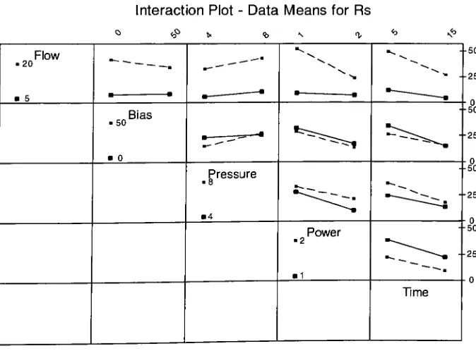
Phase diagramofTantalumandNitrogen 40Figure 2. 12: Dependenceoffactorson sheet resistance 44
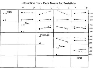
Figure 2. 13: Dependenceoffactorsonresistivity 44
Figure 2.14: Dependenceoffactorsonthickness __45
Figure 2.15: Effectofinteractions betweenfactorson sheet resistance 45 Figure2.16: Effectofinteractions betweenfactorsonthickness 46
Figure 2.17: Effectofinteractions between factorsonresistivity 46
Figure 3.1: Crosssection of samplefor TEM 56
Figure 3.2: Optical Micrographsofannealedfilmsat40Xmagnification 57
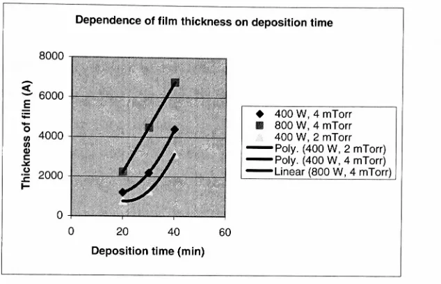
Figure3.3: Dependenceoffilmthicknessondepositiontime 58
Figure 3.4: Bl- TaN (12% N2flow)/CuonSi02/Sifilmannealedat 100
deg
C 60Figure 3.5: B2- TaN(12%
N2
flow)/CuonSi02/Sifilmannealed at200deg
C 60 Figure3.6: B3 - TaN (12%N2
flow)/CuonSi02/Sifilmannealedat300deg
C 6 1 Figure 3.7: B4- TaN(12%N2
flow)/CuonSiOVSifilmannealed at400deg
C 61 Figure 3.8:B5- TaN (12%N2
flow)/CuonSi02/Sifilmannealed at500deg
C 62 Figure 3.9: B6- TaN(30%N2
)/CuonSiOVSiasdeposited 62Figure 3. 10: B7- TaN(30% N2)/Cu onSiOVSiannealed at500C 63 Figure 3.11: Cross-sectionshowingtheinterfaceofthe
Cu/Ta2N/Si02
64Figure 3.12: SEMpicture of surface ofCuas- deposited
at20,000Xmag 65
Figure 3.13: SEMpicture ofCuannealedat450Cinsidea void 65 Figure 3.14 :SEMpictureofSurfaceofCuat450Cat80X mag 66 Figure 3.15: SEMpictureofmicrostructureofCuat500Cat20,000 mag 66 Figure 3.16: Effectoftemperatureandambientonthesheetresistance 67
Figure 3.17:
Binary
phasediagramofCuandO 68Figure 3.18: Oxidationrate of copper atvarioustemperatures 69
Figure3.19: Crystalstructureofcopperoxides(a)cubicCu20(b)monoclinicCuO 70
Figure 3.20: Schematicofdependenceofmicrostructureofsputteredfilmsonpressure, temperature 71
Figure 3.21: Stressonas-depositedfilm IN 2A 73
Figure 3.22: Stress inannealedfilm IN 1A 74
Figure3.23:
Buckling
patternonthesurfaceof copperfilms 75 Figure 3.24: Sample AlTaN (12%N2
flow)/CuonSi02/Sifilmannealed at100degC 76Figure 3.25: Sample A2 TaN (12%
N2
flow)/CuonSi02/Sifilmannealedat200degC 76Figure 3.26: Sample A3 TaN (12%
N2
flow)/CuonSi02/Sifilmannealed at300degC 77 Figure 3.27: Sample A4 TaN (12%N2flow)/CuonSi02/Sifilmannealed at400 degC 77Figure 3.28: Sample A5 TaN (12%
N2
flow)/CuonSiOVSifilmannealedat500degC 78Figure3.32: Isothermalsection of
ternary
phasediagramof(a)
Cu-Ta-Nand(b)
Ta-N-Sisystemsdrawnat900 K 80
Figure4.1:Dualdamascene architecture,PVD-depositedtantalum-baseddiffusion barriersandcopperseed
layers,
and electroplated copperfill. 83Figure 4.2: Schematicprojection view of atoms
(a)
ina unit cell oftetragonalP-Taand(b)
monoatomic layersofCuonTaattheinterfacetoillustrateatomicmatching 85Figure 4.3:
Electroplating
toolsetup 86Figure4.4:
De-plating
ofcopper seedlayer 89Figure 4.5: 5urnlinesobservedintheoptical microscope 90 Figure 4.6: SEM imageofCopperseedlayerat20,000X 91 Figure 4.7: Surfaceof electroplated copper at40,000Xmagnification 91 Figure4.8:Cross sectionshowing Electroplated
Cu,
Cuseed,Ta, Si02
andSi 92 Figure 4.9: Sheetresistance contour plot of auniformlyplated wafer __93 Figure 4. 10: Sheetresistance contour plotshowingnon-uniformplating 93 Figure4.11: Plotof sheet resistanceVstheoreticalweightdeposited 94
Figure 4.12: XRDpatternof copper seedlayer 95
Figure 4.13: XRDpattern of electroplated copper 96
LIST
OF
TABLES
Table 1.1: Comparisonof material properties 7
Table 1.2: Comparisonofrefractorynitrides andsilicides 14
Table 1.3: Comparisonof properties of variousbarriermaterials 16
Table 1.4: Comparisonof variousdepositiontechniquesforCu 2 1
Table 1.5: PropertiesofCu
"(hfac)2
andCu'(hfac)(tmvs)
22Table 2.1: FivemostintensiveXRDpeaks ofTaN 33
Table 2.2: Fivemostintensivepeaks ofTa2N 33
Table 2.3: Sputterparametersfor deposition 34
Table 2.4: PhasesofTaN
^___ 40
Table 2.5: DOErunsalongwiththeresponses measuredforeach run 43
Table 2.6:
Sputtering
parametersfor TaNfilms 49Table3.1: IDsof samples analyzed
by
XRD 58Table3.2: Physical Appearanceof sample at variousannealingtemps 68 Table 3.3:
(a)
Stackoffilmsmeasured(b)
Stressdata 73Table3.4: IDsof samples analyzed
by
RBS 75Table 4.1: Recipe for depositionof1 0,000
A
of oxide 87ACKNOWLEDMENTS
I
expressmy
deep
sense ofgratitude toDr.Santosh Kurinec for her
continuous guidanceand motivation and
for patiently answering
all my questionsduring
the course ofthisproject.
I
am grateful toDr.Dave Glocker
andDr. Vern
Lindberg
for
helping
with theIontech
Sputtering
tooldepositions.
I
acknowledgeDr.Tom Blanton
andDr.Vinnie Gupta
for
generousdonation
ofXRD
analysis and expertise.My
sincere thanks to theRichard
Battaglia,
Dave
Yackoff,
Bruce Tolleson
andDr.Illingsworth for
thefacilities
support.I
appreciate
Dr.Gabriel Braunstein for
theRBS
work andhis discussions. I
also appreciatethe
help
ofJose Medina for
theSEM
pictures,Keith Udut for
electroplating,Dilip
kumar
for
the stress measurements andFred Mathews
for TEM
analysis.I
also acknowledgeCVC-Veeco,
Inc
for allowing
sheet resistance measurements.I
am thankful toDr.
Andreas
Langner for
his
guidancethroughoutmy
masters program.ABSTRACT
As
technology
progressed toultra-large
scaleintegration
leading
to smaller and smallerdevices,
there are continuous challengesin
thefields
ofmaterials, processes and circuitdesigns. Copper is
theinterconnect
materialofchoicebecause
ofits
low
electricalresistivity
andhigh
electromigration resistance.However,
copperis
quite mobilein
silicon at elevatedtemperatures.Therefore,
topreventthediffusion
of copperinto
silicon,a
diffusion
barrier
layer
thathas fewer
grainboundaries,
good adhesiontoSi
andSi02,
high
thermal and electricalstability
with respect toCu is
necessary.Tantalum
nitridecompounds
have been investigated
as potentialbarrier
materials.TaN
has
avery high
melting
point of2950C. It is
thermodynamically
stable with respecttoCu
andhas
good adhesion to the substrate.It
has
adense
microstructure and shows good resistance toheavy
mobility
ofCu in Si
andhas
electricalstability
attemperaturesupto750
C.
The
diffusion barrier
properties ofTa
andits
nitridesfor
copper metallization atRIT
have been investigated. The
TaNx
films
were reactively sputterdeposited
onSi02
substrates at various N2/AJ- ratios.
The
influence
of nitrogen partial pressure on theelectrical and structural properties ofthe
films is
studied.It
has been
observed thatas-deposited
pureTa
is
tetragonal,
whichbecomes bcc-Ta
with smallincrease in
N2
flow
to5%
ofthesputtering
gas mixture.When
the nitrogenflow is increased from 12 up
to20%,
amorphous and amixture of amorphous and crystallineTa2N
phaseis
formed.
The
amorphous phase crystallizes when annealedtohigher
temperatures.An
fee-TaN
phaseis
formed
atN2
flow
of30%. At higher
concentrations ofN2;
nitrogen rich compoundslike
Ta5N6, Ta3N5
areformed.
During
backend
semiconductorprocessing,both Cu
andTaN
films
are subjected to variousannealing
treatmentsin
N2,
02,
andAr
at relativelyhigh
temperatures.Since
these treatments
influence
the stability ofthe metallizationit
wasimportant
to establish the effect ofthe ambients on theintegrity
ofthe copperinterconnect. The
Cu/TaN/Si02
which
is
attributedto theformation
of copper oxides with ahigh
density
ofvoids.This
was observed
by
XRD
analyis andSEM.
RBS
spectra showeddiffusion
oftantaluminto
the surface ofcopper at temperatures ~
500
to
600
C.
Therefore
we can conclude thatcubic
TaN films
act as stablebarrier films
upto500
C
in
aninert
ambient.1.
COPPER
METALLIZATION
-AN OVERVIEW
1.1
INTRODUCTION
An
integrated
circuit(IC)
or achip is
agroup
ofdiscrete
electrical devices such astransistors,
diodes,
resistors, capacitors orinductors
manufacturedsimultaneously
on a single substrate material and electrically connected to one another.The
processofconnecting
thesedevices
toeach other andtothesubstrateby
using
conducting
materialsis known
as metallization. Thehighly
conductive material calledtheinterconnect
carrieselectrical signals todifferentparts ofthesubstrate. Theperformance of an
integrated
circuitdepends
on the interconnect performance as much as theindividual
components. This requires efficient signal transmission with minimum propagationdelays
and powerdissipation
andlow loss transitionsbetweenthe
interconnection
andintrinsic devices.
Technology
has progressed to ultra large-scale integration(ULSI)
with morethanone million circuit elements on a single chip. This increase in complexityofICs
has
calledfordevelopment
intheinterconnect
technology. Whilematerials otherthanmetals have been used as
interconnects,
the term 'metallization'is generic in nature and is derived from origins of
interconnect
technology
where metals were the firstconductors used.
Currently,
several layers of materials stacked ontop
ofone another are used toform
the conducting connection betweendevices.
This processis
called multi- layeredmetallization.
For many years, aluminum and its alloys have been the industry's choice for
metallizationbecauseofits lowresistivity. Howeveras
devices
continue toshrink andinterconnect cross-sections get smaller, ahigh performance
interconnection
networkis
necessarytomatchtheperformance ofthedevicesthey
interconnect.
Suchdemand
is
reflected notonlyin
the fundamental characteristics ofthe materials usedbut
also1.2
ISSUES IN
METALLIZATION
The miniaturizationof
interconnect feature
size severelypenalizes theoverallperformance of the
interconnect,
such asincreasing
interconnect resistance and currentdensities,
whichlead
toreliabilityconcernsduetoelectromigration.With highinterconnect
resistance, the RC timedelay
will alsoincrease.Therefore,
metals with low resistivityare preferred.1.2.1
ELECTROMIGRATION
Electromigration
is
the current inducedtransportofconducting material. Thedecrease
inthickness andwidthoftheinterconnects increasescurrentdensity
throughthelines. Inthepresence ofhighcurrentstresses,electron momentumistransferred to
atoms inthe conductingmaterial,
increasing
theirmobility andyielding a net atomic flux. This net flux causes conducting material to be depleted~up
wind"and
accumulated"Mownwind"
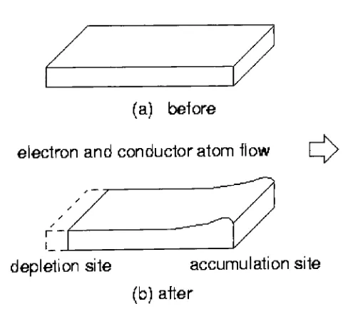
as seenin figure 1.1.
(a)
before
electron and conductor atom
flow
IZ|/
depletion
site accumulation site(b)
alterFigure
1.1: Simplifiedschematicofelectromigrationeffect on metalinterconnect
segment
[1]
Regions where the interconnect material
has
been depleted willform
a void,leading
to interconnect failure due to the formation of an open-circuit.Likewise,
[image:14.522.140.391.325.547.2]neighboring
interconnect
segments,potentially
leading
to circuitfailure due
to theformation
of a short circuit.Either
outcome can contribute to the gradual"wearing
out"
of
current-stressed
interconnects
over time. Electromigration canlead
to thebreaking
ofinterconnections
andcollapseofintegrated
circuits atlarge.The
atomicflux due
to electromigrationJatomSj
in
a single crystal orlarge-grained crystal, where the
grain-boundary
contribution to atomic diffusion can beneglected,
is
given asJatoms
=NDZ'qj
/ (rkT)
(1)
where
N,
D,
Z*,
q,j,
r,k,
and T are atomicdensity,
atomicdiffusivity,
effectivecharge on the moving
ions,
electron charge, currentdensity,
electrical conductivity,Boltzmanns
constant,andtemperaturein degree Krespectively.[2]
The
diffusion
of metal atoms in polycrystalline materials predominantlyoccurs along grain
boundaries
that usually have higher diffusivities than the grainlattice. This current induced
diffusion
can lead to void and hillockformation.
Voidformation
canlead toan opencircuit, whileahillock,
which extendstomake contactwith another
interconnect
line,
can lead toa short circuit. Eitherofthesewill lead to circuitfailure.
Thefailure
rateis
often modeled empirically, with thefollowing
equationfor
theMedian Time To Failure (MTTF):MTTF= A
J"n
exp
( EA/kT)
(2)
where J
is
the currentdensity,
n istypically
close to2,
and A is a constant, whichdepends
onfilm
structure(
grainsize, etc.)and processing.EA
istheactivationenergyfor
electromigration and is often associated with grainboundary
diffusion
(theactivationenergy oflattice diffusion in bulkaluminum films isabout 1.4eV while
it
is 2.19
eV forcopper). Theparametersforthisequationareusuallydetermined
underaccelerated
testing
conditions that employ higher than normal current andtemperature. Accelerated
testing
isalso usedto predict when shorts or opens occurin
theinterconnect
lines
orwhenthelineresistancereachesa critical value.Electromigration can be reduced
by increasing
the grain size of thediffusion
across the grainboundary
by
addition of solute atoms, orby
choosing analternative metallization scheme
-withthereplacementof aluminum withcopper.
1.2.2
RC DELAY
As the
feature
sizedecreases,
thereis
an increasein
chip size. This causes anincrease in length
of theinterconnects,
leading
to higher resistance. Thereis
adecrease in
thedistance between
adjacentinterconnects
leading
to an increase incapacitance
between
them although there is a decrease in capacitance between theinterconnect
and ground substrate, resulting in an increase in the total interconnectcapacitance atthe submicron range.
Since
both line resistance, R andcapacitance, Cassociated with the
dielectric
contribute to interconnectdelay,
the total interconnectdelay
increases
rapidly. As devices become smaller, RCdelay
will increase thecarrier transient time, which will be a major obstacle to
increasing
the speed ofthechips.
The RC
delay
isgivenby
RC= pL slLD/tu tiLD(3)
wherep,Land
tM
arethe resistivity, lengthandthicknessoftheinterconnect,
andsh,dand
t^D,
the permittivity and thickness of the interconnect dielectric(ILD)
respectively.
[2]
It is estimated that in the sub-micron range the total interconnectdelay
increases rapidlywithdecrease in feature sizeasshownin figure 1.2.IntrinsicGate
Delay
-0.0 0.5 1.0 1.5 2.0 2.5 3.0 3.5
Feature Size
(urn)
There
are two solutions to overcome this problem.One
approachis
to lower thecapacitance
by
using low
permittivity
materials(also
called as 'lowk
dielectrics')
asinterlevel
dielectrics.
The
otheris
touseinterconnect
materialswith
lower
resistivity.1.3
NEED FOR A
NEW
METALLIZATION
Aluminum has been commonly
used asmetallizationmaterial asit
meets most ofthemetallization requirementsfor
LSIdevice:
it has
arelatively
lowelectrical resistivity.it has halide
compounds with arelatively
high pressure, which are suitablefor
reactiveion etching (RIE).
it
canform
a thin protective oxidefilm
that withstands various thermal process andhas
a goodadhesiontooxide.it
has
a goodstepcoverage.it
is
aninexpensive
material.For sub0.5 pm
technologies,
aluminumdepositedorreflowed at temperaturesexceeding
450C
is a means to achieve planarization.Usually,
a layer ofdiffusionbarrier
is needed to prevent diffusion ofAl into Si. The high temperaturesinvolved
during
deposition
place a stringentdemand ontheintegrity
ofthe barrierto preventjunction
spikingcausedby
Al/Siinterdiffusion [21]. TiN is presentlyconsideredtobethe
barrier
material of choicefor
sub-0.5 pmmetallization. Formetallization ofVLSIcircuits, Al suffers
from
majorlimitationsthat areduetoboth properties ofthemetal and deposition techniques. One of the mostimportant
reliability problemsis
electromigration discussed in section 1.2.1. For thedevelopment
of ultra-large scaleintegration
(ULSI),
theelectrical resistivitiesofAl andits
alloys are notlow enough.As the minimum geometry
is
scaled down to one-quarter micron, Al andits
alloysAn interconnect
material shouldmeetthefollowing
requirements:Low resistivity
Void free deposition
onhigh
aspectratiotrenchesand viasHigh deposition
rate andeasycontrol of microstructuresEase
ofpatterning
and planarizationGood
adhesiontointerlayer dielectrics
and other materials on achipLow reactivitywithenvironment,and
Low stress andhighresistancetoelectromigration and stressinduced voiding
Cu
Al
Au
Ag
Resistivity
(pQ
cm)1.67
2.66
2.351.59
AR/ATat0-100C(10-3/K)
4.3
4.5
4.0
4.1Melting
Point
( K)
1083.4
660.1
1063 960.8At. Wt
(amu)
63.54
26.982 196.967 107.868Youngs Modulus
(GPa)
129.8
70.6 78.5 82.7Yield
Strength( MPa)
216 55 130 172Hardness
(HV)
51 1.5 20-30 25Do
(cm2/s)
at 100C
0.78 1.71 0.67 1.89Activation
Energy
(eV)
for
diffusion
2.19
1.48 1.96 2.01D
Diffusivity
(cm2/s)
at 100C
2.1 x 10"30 2.1 x 10"20 2.2x 10"27 1.1 x 10"26Delay
(psmm"1) 2.2 3.7 3.2 2.2Thermal
Conductivity
(W/cm)
3.98 2.38 3.15 4.25
Depositionand
Etching
Sputtering
Yes Yes Yes YesEvaporation Yes Yes Yes Yes
CVD
Yes Yes(?)
? ?Plating
Yes ? Yes YesWet Etch Yes Yes Yes Yes
Dry
Etch?
Yes ? ?Electromigrationresistance High Low High
Very
lowCorrosionresistanceinair Low High
Very
high Low1.4
COPPER
METALLIZATION
Resistivity
ofCu
is
about40%
less
than that of Al. Ithas
high electromigration resistance.The
selfdiffusion
of copperis
also the smallest among thefour
elements,resulting in improved
reliability. Although alot
ofresearchhas
been done
on copper inthelast
several years, only recentlyhas
theindustry
begunto consider it as afeasible
production technology. The IBM CMOS 7Stechnology
illustrated
infigure
1.3 was thefirst
process tointegrate
Cu in aCMOS technology.[4]
Figure
1.3:
CMOS7S
- ASIC showingsixlevels
ofcopperCu
metallizationhas
thefollowing
advantages:Reduced
RC
timedelay
Cu has
a lower resistance that that of Al.Therefore,
RC timedelay
is
reducedenablingthesignalstomovefaster.
Since Cu is
abetter
conductorofelectricity
comparedtoAl,
Cu interconnections
canbe
made narrowerto0.1
micronsinstead
of0.25
microns.Hence,
thepackingdensity
will
be increased. It is
possible tohave 150
200
million oftransistors on a singlechip.
Subsequently,
therewillbe
anincrease in computing
power as well.Reduced
power consumptionCu lines
canbe
made thinner to execute the samefunction
as Al. As thefilms
getthinner,
the capacitance onthe chip, whichisprimarily
sidewall capacitance betweenthe adjacent
lines
of Cuis
less.
This
helps to reduce the amount of powerconsumptionifthin
Cu lines
arecombinedwith amoderately low-k dielectric.Superior
resistancetoelectromigrationAs wiring
linewidths
decrease,
currentdensity
carriedby
thoselines,
whichis
thedriving
force for
electromigration,increases.
However,
Cu hasa superior resistancetoelectromigrationwhen comparedtoAl. It isreportedthat theelectromigration
lifetime
for
Alis
inorders of magnitudehigherthan that ofCu. This is important for ICsusedinnon-temperature-regulatedenvironments.
Prevent
circuitsfrom
overheatingCu
is
also a better conductor of heat. It can prevent damage to the circuits fromoverheating.This has alsomadeitpossibletohaveclosepackingoftransistors.
1.4.1
DISADVANTAGESOF
COPPERCopper
is
afast
diffuser in silicon. It can form three acceptorlevels
in themiddle of silicon band gapat
0.24eV,
0.37eV and0.52eV with respectto thevalence edge. Thesedeep
energy levels provide a mechanism for excess minority carriersrecombining with majority carriers [5].
Consequently,
Cu willinduce
generation-recombination leakage current in p-n junctions andjeopardize the performance ofbipolar
transistors,leading
to a reduction in current gain. Copperinduced leakage
current can alsolimittheperformance oflight detectorthatconverts a photo
flux
toacharge packet or electric current. A high concentration of Cu near the Si
-Si02
Copper forms
silicides,Cu3Si, by
reacting
with the substrate at temperatureless
than200C. After
theformation
oftheCu3Si
phase, theunderlyingsiliconin
theCu3Si/Si
structureis readily
oxidized even at roomtemperature,
resulting in rapidgrowth of a
layer
ofSi02
uptoafew
micrometersinthickness.[6]
Unlike
thecaseofaluminum whichforms
apassivatingoxidelayer,
copperis
readily
oxidizedtoform
aCu20
andCuO
phases attemperaturesabove 100C
and noself protectiveoxide
layer forms
topreventCu from further
oxidation. Theoxidationrate
depends
on the orientation of copper surface. The mostlikely
orientation planesare
(100), (111)
and(110),
with the(100)
planehaving
the highest oxidation rate.The
lack ofself-passivation makes a copper thinfilm
susceptibletooxidationduring
processing. Ifcopper
is
oxidized, theresistance ofCuinterconnects increases
rapidly.Therefore,
Cu should notbeexposedtoair athightemperaturesatanystage.Copper reacts at low temperature with most metals, such as
Al,
Au andPd,
which are commonly used in microelectronic
devices.
CuAl2
can be formed in aCu/Al bilayer structure. At 150
C,
Cu reacts with Au to formCuAu,
Cu3Au andreactswithPdto
form
Cu3Pdcompound at200
C.
Copperalso reacts readilywithmostsilicides,such as
CoSi2,
CrSi2,
andTiSi2,
at temperature below 450
C.
Cu can diffuse throughCoSi2
toform
Cu3Si at theCoSi2/Si interfacewhile the
integrity
ofCoSi2
layeris
maintained. IntheCu/CrSi2/Si
system, Cu3Si forms on
top
ofCrSi2,
dueto siliconmigration, toreactwithoverlyingCu. Cu can induce partial decomposition of
TiSi2
to form Cu3Ti and Cu3Si in theCu/TiSi2/Sistructure.
Copper layers exhibit poor adhesion on both silicon dioxide and polymer
substrate. In general, interfacial adhesion is strongly related to the
bonding,
surfacemorphology, and stress relaxation attheCu/substrate interface.
Annealing
a Cu filmon a
Si02
substrate causes thefilmtopeelundertensilestress. Whencopper contactsapolymer, such as polyimide, copper
forms
a weak chemicalbond
with polyimideand diffuses into
it
to form agglomerates at low temperature.However,
it has been
reportedthatsputteredcopper
films,
depositedon clean and moisturefree
surfacesin
equipment pumped down to a very high vacuum of
10"6
-10"7
Pa show reasonable
adhesiontoboth
Si02
andpolymerfilms. Mostofthempass theScotchtapepeel testin
the as-deposited condition,but
onannealing
athigher temperatures,
peelingis
observed.
The
latter
effectis
related to thedifference
in
thermal expansioncoefficientsof
Si02
andCu.
To
avoid aforementioned problems,diffusion
barrier,
passivationlayer,
andadhesion promoter are needed.
The
ultimate objectiveis
to find a diffusion barrier materialbetween
copper and theinterlayer dielectrics
that will also perform as anadhesion promoter.
Fortunately,
there are manydiffusion
barriers thatare also good adhesionpromoters.1.4.2
PATTERNING OF COPPER
Copper is difficult
toetch. The maindifficulty
ofusing conventional plasmaetching
to patternCu
is thelack
of Cu compounds that are volatile at lowtemperatures. Wet etchingandlift-off
techniques,
usedinaresearchenvironment, areinadequate for
submicron geometries.1.4.2.1 Wet etching
Coppercanbeattacked
by
variouschemicalsthatcanbeusedforetching.Oneexampleis an aqueous solution of ammonium persulfate and ammoniumchloride. A mixture of 500 cc deionized water, 45 gm ammonium persulfate and 3 gm ammonium chloride etches copperattherate of about 1000nm/min. Sincewet etch
is
anisotropic
process, thereis large undercutting makingprecisecontrol oflinewidthimpossible.
Therefore,
wet etchis
not suitableforsubmicron coppermetallization.1.4.2.2 Plasma etching
Plasma etching isthemostwidelyused methodfor patterning Al-alloys. It has
several advantages over wet etch. It gives anisotropic etching, which minimizes undercut, andthere
is
agood controloftheetchingrateandtime.It
is
difficulttodo
plasmaetchingofcopperbecausethecopperhalides
are not1.4.3
CHANGES
IN
PROCESS
TECHNOLOGY
WITH
COPPERMETALLIZATION
Copper has
a superior resistance to electromigration, whichis
a commonreliability
problem in aluminumlines
at thedeep
submicron level. This means thatcopper can
handle higher
powertransistors,
whichbroadens its
applicationtoawholenew range of
analog devices.
Themainchallenges ofCu
interconnects
aredifficultiesin line
patterning andpotential
device
contamination. Theseproblems are overcomeby
use ofbarrier layersbetween
Cu and the substrate and a new strategy called the damascene or'inlaid'
patterning to
form
theinterconnect
lines. The damascene approach requires 20-30%fewer
steps than traditional subtractivepatterning(by
etching). This also reducesthecost of manufacturing.
The second way copper can reduce costs is thatbecause smaller lines can be
used to carry the same amount ofcurrent, atighterpacking
density
can be achievedper level. This means that fewer levels of metals are needed, which leads to a
significantdecrease in manufacturingcosts.
16
14
12
r 10
E 8
0)
B
04-Reduced
Complexity
Cu,low k
* AluminumSi02
0.1 0.2 0.3
Technologygeneration(um)
0.4
Figure
1.4: Plot
ofNo.ofmetallayers
vs. FeatureSize
1.5
DIFFUSION BARRIERS
Diffusion barriers
are thinfilm layers
used to prevent two materials fromcoming into direct
contactin
orderto avoid reactions betweenthen.Ideally,
abarrierlayer X
sandwichedbetween
AandB shouldpossessthefollowing
attributes.[7]
Itshould constitute a
kinetic barrier
to themovement ofAandBacrossit.
i.e.,
thediffusivity
ofAandBin
XshouldbesmallIt should
be
thermodynamically
stable with respect to A and B at the highesttemperatureof use.
Further,
thesolubility ofX in AandB shouldbesmall.Itshould adhere welltoandhave lowcontact resistance withAandBand possess
highelectrical andthermal conductivity.Practical considerations alsorequirelow
stress,ease ofdepositionandcompatibilitywith otherprocessing
A
large
number ofmaterials have been investigated for use as barrier layersbetween
silicon and copper. Aconsiderationforthechoiceofdiffusionbarrier isthatit be
metallurgically stable with respect to the metal that carries current. This is aneasy condition to meetfor copper, since many refractory metals do not form copper
compounds.
However,
coppermaypenetratethrough ametal withoutreactingwithit.Selection of such a material starts with an investigation of mutual
diffusivity
andinteractions. Since
diffusivity
isdirectly
related tomelting point ofthe material, thebest diffusion barriers have the highest melting point.
Also,
the high activationenergies associated with diffusion through refractory metals is the dominant factor.
Refractory
metals like titanium, tantalum and tungsten and their nitrides, carbides,silicides andboridesact asgoodbarrier layers.
We see from table 1.2
[18]
that the melting temperature and theheat
offormation ofnitrides
is
higherthan that ofsilicides, whereasthe electricalresistivityand schottky barrier are comparable. It
is
due to their superior thermal stability thatProperty
TiN
TiSi2
TaN
TaSi2
Crystalstructure
fee
orthorhombic Hex. Hex.Tm
-Melting
temp
(C)
2950
1500 2950 2200A
H29g
.Enthalpy
offormation
(kcal/mol)
-80.4 -32.1 -60.3 -28.5
p-Resistivity
(
pQcm)
20-70 15-25 135-250 10-50Bn
Barrierheight
0.49
0.6 0.59Table
1.2:
ComparisonofrefractorynitridesandsilicidesSingle transition metal films are usually polycrystalline.
They
are stable as barrier between CuandSi totemperaturesofaround500C
(forPd,
CrandTi)
to650
C
(for Ta). Cu reacts with near noble metals such asCr, Co, Ni,
Pd and Pt in thetemperature range of 250
C
to 450C
but is non-reactive and immiscible withrefractory metals such as
Mo,
TaandW. The near-noble metalsalso react withSito form silicides atlowtemperaturesbetween 100- 450
C,
while therefractorymetalsdo not react up to 525 -
650 C.
The failure mechanism is usually due to the highreactivitiesofbarriermetal- CuorSi- barrier
metal,followed
by
Cu-Sireactionforthe metals in the first group and diffusion of Cu through grain
boundary
of thepolycrystallinebarrier films atrelativelylowtemperatureforthemetalsinthesecond group.
So,
transitionmetalsarenot stablediffusion barriers between CuandSi.[8]
Theeffectiveness of silicidesortransitionmetal
-siliconsystems asdiffusion
barriers followsatrendsimilartothatoftheircorrespondingtransitionmetaldiffusion
barriers,
butthesilicidesarebetterby
100to200C.
The diffusion barriers formedby
refractorymetal
(
Ta andW)
- Si are most stable upto 450 to700C
than thoseby
near noble metal (Cr andCo)
- Si barrier which are stable only to about 300C.
Adding
silicon to refractory metals to form an amorphous refractory metal - Sidiffusion barrieralso improvesbarrierperformance. The barriers fail
by
the reactionof Cu with the silicide barriers to form Cu
-silicide,
by
Cu diffusion throughpolycrystallinetransitionmetal silicides, or
by
Cu
-induced
premature crystallization
oftheamorphous metal silicon
barrier films.
The
metal-nitrogen systems of Ti
-N,
Ta- N and W N show ahigh
stability
asdiffusion
barriers.
This is due
to thenon-reactivity
ofCu withN,
TaandW. Barrier failure is
causedby
thediffusion
ofCu along
the grainboundaries
orthrough
defects
generated at elevated temperaturein
thebarrier
films,
which arerelatively
intact,
orby
reactionbetween barrier films
and Si toform
metal -rich
silicides.[8]
1.6
BARRIER
MATERIALS
The
following
are thecommonly
used barrier materials between copper andsilicon.
1.6.1
TANTALUM
Tantalum
is
a greyish silver,heavy,
and very hard metal. It has a meltingpoint exceeded only
by
tungsten and rhenium. The bulk properties of tantalum arelisted in
table 1.3and compared with otherrefractorymaterials.Ta
is
stable as abarrier up to600
deg
C.Among
six transition metals ofCr,
Ti, Nb,
Mo,
TaandW,
only TaandWretaintheirinterface
withCuafterannealingat600
C
for
1hour.
At higher temperatures,a complex reaction occursthatinvolves
themotion of all three elements. Cupermeated the Ta
film
toform
Cu3Siprecipitates attheTa-Si
interface,
andtheTareactedwith the Si substrate toforma planarlayer
ofhexagonal
-TaSi2.
Thestable state ofbulk Ta hasabccstructurewitha
lattice
parameter of3.298A.
However,
athin sputteredTa filmtypically
hasa metastablep
- Tastructurethat
has
atetragonalcrystal structure. Heteroepitaxial growth ofCu in-situdeposited
onp
Ta has
beenreported [27]. The[220]
direction ofCu (1 11)
planeis
observedtoline
up with the
[330]
direction ofp
Ta(002)
plane with a misfit strain of7.6%. As
aresult, Ta
has
better adhesionwith Cuand results in a strongerCu texture thanTiN.
Although Ta
is
typically
depositedby
sputtering, plasma assisted chemical vapor1.6.2
TANTALUM NITRIDES
The barrier
properties of Ta canbe further improved
by
the addition ofimpurities
to thefilm.
Ifthesolubility limit is
exceeded, solute atoms in a Tagrainwould
be
expected to segregate to the grainboundaries,
obstructing thesefast
pathways
for
copperdiffusion.
Property
Ti
TiN
Ta
TaN
Melting
point(deg
C)
16682930
3014 3087Thermal
coefficient ofExpansion
(deg
C)
8.6
x 10"6 9.4x 10"66.5
x 10"6 5.6x 10"6Electrical
Resistivity
(p-ohm cm)
40 1100-1800 (depends
on
%N)
14.7 160 (for 20%
N)
Thermal conductivity (cal/sec-cm-degC)
0.22 0.544 0.046
Stresses
inCu/x/Si02
x-Diffusion barrier
Tensile Compressive Compressive Compressive
Barrier
Stability Temp
0fCu/Si/Si02(degC)
450 550
600
650-750
Methods of deposition
Sputtering
yes yes yes yes
PhysicalVapor
Deposition
(PVD)
Yes for Al
No
for
CuYesfor Al
No for Cu
Yes for Al
No for Cu
Yes
for
AlNo for Cu
Chemical Vapor Deposition
(CVD)
Sameas PVD Sameas PVD Sameas PVD Sameas PVD Activation energy(eV)
Al-Ti: 1.8 Cu-Ti: 3.2 Al-TiN: 1.2 Cu-TiN:2.5 Al-Ta:2.3
Cu-Ta: 1.5Cu-TaN:
4.4Phases
hep
bcc-polycrystalline,
columnar
bcc-P
Ta
columnar-Crystalline
fee,
amorphous
Table 1.3:
Comparisonofpropertiesof variousbarrier
materialsFor
a nitrogen concentrationbetween 10-20
%,
Ta2Nis
present along withbcc-
Ta
phase. Anamorphous component appears at around 15 %. The structure of
tantalum nitrides can
be described
as close-packed arrangements ofTaatoms withN
atoms
inserted in interstitial
sites.The
space group ofTa2Nis
P63/mmc,
with equalnumberof sites
for
TaandN
atoms,whilethenitrogen atoms occupy halfofthe sitesrandomly.
However,
deviations from
thisoccupancy
ratio can occur, which explainsthe
finite
range ofexistenceofTa2N.
It
has been
reported that tantalum nitrideshave better
barrier properties thanTa or TiN. TaN
is
stable with Cu up to 750C.
In PVDTaN,
the phases ofTaNx
changes
from
p
Ta tobcc-Ta,
then amorphousTa2N,
and non-crystalline TaN tocubic TaN withthe
increase
ofN2
flow.
Thesuperior barrierproperties ofTaNoverTa are due to the stable TaN compounds. CVD TaN
has
better step coverage thanPVD
TaN,
butthedeposition
temperatureofCVD TaN is 450-650C
thatis too highfor
back-endprocesses.1.6.3
TANTALUM-SILICON-NITRIDE
Ta-Si-Nhasan amorphous structure. SinceCu diffusion
is
fasterthroughgrainboundaries
than through crystal bulk lattice in barrierlayer,
an amorphous layer hassuperiordiffusion barrier property overapolycrystallinelayer. Ta-Si-N is stable as a
barrier upto 900
C.
The crystallization temperatureis
higher than 1000C,
butthebarrier failsat around900
C
by
premature crystallization whenTa-Si-Nis
incontactwith Cu. Under identical sputtering conditions, Ta-Si-N films have superior step
coverageoverTiN.
However,
compositional variation isaconcernfor Ta-Si-N filmsin
trenchesand vias.1.6.4
TUNGSTEN NITRIDESAlthough Ta-based materials have good barrier properties on
Cu,
Chemical
Mechanical Penalization
(CMP)
ofTawithoutdamaging
Cuis
verydifficult.
During
the
Ta
CMP,
dishing
andoveretchingofCuareverysignificant. Comparedto theTa-based barrier
layer, WNX
is
more appropriatefor CMP.WNX
CMPcanbe
performednicely
evenwiththesame chemicals usedin Cu CMP.Furthermore,
plasma enhancedCVD
is
availablefor
WNX,
which gives excellent coverage. W2Nis
stable as abarrier
cm.
However,
amajor concernofWNX
inCu
metallizationis
thepoor adhesion ofCuon
WNX
films.
1.7
DAMASCENE
PROCESSING
The
practice ofcreating
patternsby
metalinlays
wasfirst developed
by
theancient artisans of
Damascus.
A similar process called Damascene processingis
being
adoptedby
the semiconductorindustry
to createinterconnect
linesby
first
etching
atrench or canalin
a planardielectric
layer,
andthenfilling
that trench withametal. In
dual damascene
processing(figure
1.5),
a secondlevel is involvedwhereaseries of
holes
(i.e.,
contacts or vias) are etched andfilled
in addition to the trench.After
filling,
themetal anddielectric
are planarizedby
chemical mechanicalpolishing(CMP).
The main advantage of
damascene
processing is thatit eliminatesthe needfor metaletch. This
is
very usefulbecausecopperis
difficulttoetch.Asecond advantageisthatit
eliminatestheneedfordielectric
gap fill.[10]
Ban tet
deposition
<o&2. Iritemiinnaet
lithography
aSttrtraeliwmaineteii
1, Pifetartrfe(jug!(feijnaiiscfjg
itrifcrtsflnMsl
IO
EZZ
i-&i^Tatarts tfGu
candutifirtiir/gf 3,iteripatiCmfill
Barrier
4, Rfefrtwe
WtJipfig
Cujbarrier
by
NB>(taflfawSil'*ik-ilW!if*i !
1.8
CHEMICAL
MECHANICAL
PLANARIZATION
(CMP)
As
the semiconductordimensions
continue to shrink, modemphotolithography
equipment approachesits depth
offield
limits. Slight irregularitieson thewafer surfaceor on
deposited films
candistort
semiconductor patterns asthey
are transferred
by
alithographic
process to the wafer surface. Chemical MechanicalPlanarization has
evolvedasthepreferredmethodfor preventing distortion.This
involves planarizing
the wafer surface to aflat,
uniform finishby
use ofan abrasive suspendedina chemicalslurryand a circular
(sanding)
actionas showninfigure
1.6.Conventional
systemsapplytheslurrywithrotating disksabove andbelowthe wafer. When the wafer
is
uniformly planar, photolithographic patterns can betransferred with minimal distortion. In complex semiconductors with multiple
interconnect
layers,
CMP systems are used after each conductive or dielectric layerhas
beendeposited
toprepareit
forthenextphotolithographic step.Chemical Mechanical Flanariz
erSide View
Top
View
SlimyFeed
^^^
1.8.1
CMP OF
COPPER
Planarizing
copperis
aschallenging
as the process ofdepositing
copperfor
damascene
interconnect
structures.Copper CMP for damascene
structureinvolves
developing
apolish process thatminimizesthepatterndensity
andfeature
size effectsassociated with typical
CMP
processes.Development is
complicatedby
new barriermaterials,
lack
ofcommercial slurriesandthematerial properties of copperitself.
Copper is
a material thatis difficult
to polish. Itis
soft and subject toscratching
and embedded particlesduring
polishing. Alsobecause
copper ishighly
electrochemically
active anddoes
notform
a natural protective oxide, it corrodeseasily.
Therefore,
protecting
the copper surfaceduring
polish, clean and subsequentprocessing
isessential.Copper CMP is
also more complexbecause
ofthe needtoremovethebarrierlayer
and copper uniformly withoutoverpolishing
anyfeatures.
This isdifficult
because
current copperdeposition
processes are not as uniform as the oxidedeposition
processes.1.9
DEPOSITION OF COPPER
As the
damascene
process is adopted, voidfree
trench and via - fillbecome
the most critical requirement for deposition of copper. In table 1.4 four deposition
methods are compared with thiscriterioninmind.
Properties
CVD
PVD
Electrolytic
plating
Electroless
plating
Impurities CO Ar
Seed
LayerDeposition Rate
(nm/min)
100 100 200 -100
Process
Temperature
(C)
250 Room Room
50-60
Step
Coverage Good Fair GoodGood
Via-Filling
Capacity
Good Poor Fair Fair
Waste
Good
Good
Poor
PoorCost
High
High
Low
LowTable 1.4:
Comparison
of variousdeposition
techniquesfor Cu
1.9.1
PVD OF COPPER
Sputtering
is
an easyPVD
method ofdepositing
copper. The sputteryield ofcopper
is among
thehighest
of all the metals. At600
V argon ion energy, thesputtering
yield(atoms
of copperdeposited
perion
ofargon)of copperis reported tobe
2.8,
compared with 1.2 for Al and0.6 forW.[3]
Forviafilling,
and planarizationusing biased
sputtering,suchhighsputtering
yields couldbeadvantageous.Conventional
PVD techniques are not adequate for Cu deposition into highaspect ratio trenches because
keyholes
would from inside the trenches. The largeangular distribution of sputtered atomicflux will pinch offCu film at the
top
ofthetrenches
during
deposition. Toovercomethis problem,eitherhightemperaturereflowafter sputtering or directional sputtering techniques such as ionized sputtering or
magneticfieldenhancedsputteringmay beemployed.
Although sputtering
is
not a suitable process for Cuinterconnection,
a thinsputtered Cu filmcanbeused as a 'seed layer"
forotherCu depositionprocesses.The
seed layer provides an atomically smooth and cohesive copper interface that
encourages correct graingrowth
during
thesubsequentbulkcopperfill step.1.9.2
CVD OF
COPPERChemical vapor deposition
(CVD)
has been extensively used in the ULSItechnology
duetoits
superiorstep coveragetophysical vapordeposition. CVD
is theformation
ofa single compoundon a substrateby
thermalreaction ordecomposition
of gaseous compounds, which contain the required constituents. For
Cu
CVD,
metalorganic precursors are commonly used,
i.e.,
MOCVD (MetalorganicChemical
Vapor Deposition),
becauseit
allows deposition at relatively low temperatures.Several
metalorganic precursors have been exploredfor Cu deposition. Cu
u(hfac)2
represents
hexafluoroacetylacetonate,
and the tmvs represents trimethylvinylsilane.Properties
oftheseCu
precursorsarelisted in Table
1.5.Cu
u(hfac)2
Cu
I(hfac)(tmvs)
State
Solid
LiquidDecomposition
temp
>200
C
>40CVapor Pressure
- 10 Torrat 100
C
-0.3
Torrat40
C
Reaction
Reducing
agent required DisproportionationreactionConversion
tocopper Inefficient EfficientDepositionrate - 10-20
nm/min -200nm/min
Depositiontemperature -250-400
C
-150-180C
Table 1.5: Propertiesof
Cu
n(hfac)2
andCu'(hfac)(tmvs)
Cu
n(hfac)2
is asolid at room temperature. Itexhibits good thermal stability,but
its
vaporpressure is not adequate atlow temperatures(
< 100C).
Temperatureshigher than 200 - 300
C
are required to get a reasonable deposition rate. The decompositionofCu
n(hfac)2
topureCurequires reductionby
hydrogen. Thereactionis
shown as follows:-(4)
Cun(hfac)2(g)
+H2(g)
-*Cu
+2Hhfac
(g)
The enthalpy forsublimation
is
13.2 kcal/moleCu
'(hfac)(tmvs)
is
a pale yellow liquid at roomtemperature. The depositionefficieny of
Cu'(hfac)(tmvs)
is
muchhigher than that ofCu"(hfac)2,
which allows deposition ofCu at lowertemperatures and higherrates. At temperatureslower
than150
C,
the deposition rateis
very low. Since film resistivity increases exponentiallywith temperatureabove 150
C,
150 - 170C
is
the the optimum temperaturerangefor
Cu deposition.[13]
The depositionreactionsteps ontheheatedwafer surfaceare as
follows:
2CuI(hfac)(tmvs)
(g)
-*2Cu'(hfac)(tmvs)
(s)
2CuI(hfac)(tmvs)
(s)
-}2Cu'(hfac)
(s)
+2(tmvs)
(g)
2Cu'(hfac)
(s)
-*Cu(hfac)
(s)
+Cun(hfac)
(s)
Cu(hfac)
(s)
+Cun(hfac)
(s)
->Cu
(s)
+Cun(hfac)2 (s)
-(5)Physical
vapordepositions
aredifferent from
chemical vapordepositions
inthe
deposition
mechanism. Thedeposition
ratefor
CVD will be proportional to thedeposition
temperature.However,
thedeposition
ratefor
PVDwillgenerally decreasewith
increasing
deposition
temperature.1.9.3
ELECTROLESS PLATING
During
the early stages of Cu processdevelopment,
electroless plating ofcopperdrew attention
because
itoffers a simple andcheapprocess andthepossibilityof selective
deposition
whichmayeaseline definition.Inelectroless
deposition,
Cuatoms are suppliedto thefilmsurfaceby
catalyticreduction of aqueous
ions.
Sinceelectrons for Cureductionare providedby
oxidationofthereducing agent in the deposition
bath,
and this oxidation is catalyzed only atconductive surfaces, electroless Cu deposition is
inherently
selective on conductivesurfaces.Atypical Cuelectroless processis
Cu+2+2HCHO+40H -* Cu +
H2
+2HCOO +2H20(6)
where copper
ions
aresuppliedfromthecoppersulphate(CuS04.5H20)
solution.The growth of electroless Cu
is
highly
dependent on the seedlayer. Cu
nucleation
is
very poor on Ti. The adhesionis
poor on W. OnTiN,
eitherisland
deposition or rough surface
is
formed. Pd2Siis
an excellentseed layerfor
electrolessCu deposition. A thin sputtered orCVD Cu layer
is
perhaps thebest
seedlayer for
electrolessplating.
1.9.4
ELECTROLYTIC PLATINGWith the capability of Cu
CMP,
voidfree
trenchfilling
becomes
a moreelectroplating
is
better
than that of electrolessplating because
the depositionparameters can
be easily
controlledin electroplating
while deposition progressesspontaneously
according
to thechemistry
of theplating bath.
By
modulating thecurrent
flow direction in electroplating, both deposition
andetchingare possible.
Cu electroplating is
ascheap
andsimple as electroless plating. The depositionrate
is
also veryfast, typically
faster
than3500
A/min.
It also has a excellentcompatibility
withlow
- Kmaterials
because
thedeposition
temperatureis
low, i.e.,
roomtemperature.
Electrodeposition
of metalis
theprocess ofdeposition
of metalby immersing
aconductive surface
in
asolutioncontaining ions
ofthe metal tobe deposited. Thesurface
is electrically
connected to an external power supply and current is passedthrough the surface
into
the solution. This causes reaction of the metalions
(Mz+)
with electrons
(e~)
toformmetal(M)
Mz+
+ ze ->M
(7)
In the case of electrodeposition of copper onto a silicon wafer, the wafer is
typically
coated with a thin conductive layer of copper seed andimmersed
in asolution containing cupric ions. Electrical contact is made to the seed
layer,
andcurrent
is
passed suchthat thereactionCu2+
+2e"^ Cu
(8)
occurs atthe wafer surface. The wafer, electrically connected so thatmetal
ions
arereduced to metal atoms, is referred to as the cathode. Another electrically active
surface, the anode, is present in the conductive solution to complete the electrical
circuit. Atthe anode, an oxidation reactionoccursthatbalancesthecurrentflowatthe
cathode, thus maintaining electrical neutrality in the solution. In the case of copper
plating, all cupric ions removed from solution at the wafer cathode are replaced
by
dissolution
from
a solidcopper anode.Electroplating
canbe
carriedoutusinga constantcurrent, constantvoltage, orvariablewaveformsofcurrentofvoltage.
Using
a constantcurrent,accurate control ofmass ofthedepositedmetal
is
mosteasily obtained.Plating
at a constant voltageandusing
variable waveforms requires more complex equipment and controlbut
canbe
useful
in
tailoring
specificthicknessdistributions
andfilm
properties.[11]
1.10
ANALYSIS
TECHNIQUES
TO TEST BARRIER STABILITY
The
properties ofthebarrier film like
the electrical resistivity,density,
grainstructure,
defect
distribution
and stress vary significantlydepending
on theirdeposition
techniques andprocessing
conditions.So,
this causes a change in theirmaximum temperature of
stability
of barrier (Ts). Another reasonleading
to thevariability
ofTs
is
theapplicationofdifferent
analysis techniques.Many
conventionalcharacterization
techniques,
including
Rutherford
Backscattering
(RBS),
Secondary
Ion Mass
Spectroscopy
(SIMS),
X-ray
PhotoelectronSpectroscopy
(XPS)
andAugerElectron
Spectroscopy
(AES),
have
been used in almost all barrier performancestudies and actto measure themetallurgical stability. Withthese
techniques,
it isnotnecessary
topattern silicon.Therefore,
they
arevery convenient.However, they
lackgreatsensitivityas well asdirect applicabilitytoelectrical performance.
Electrical characterization such as bias thermal stressing, or study of I-V
characteristicsprovides greater sensitivity for quantifying the barrierresponse. Thus
electrical characterization will indicate the onset ofan
instability
before otherless
sensitive techniques.
Usually,
the realTs
is
50 to 100C
below theTs
obtainedby
conventional analysistechniques.
[8]
1.11
CONCLUSIONCopper will replace aluminum as the main interconnect metal in the next
decade.
Various transition andrefractorymetals, their alloys, silicides, nitride, oxideand
ternary
barrier are studied as potential diffusion barriers. Itis
veryimportant
toevaluate
thoroughly
the various barriers and optimize theproperties and depositiontechniques.
Also,
it is
necessary to understandthechangeinprocesstechnology
with2.
REACTIVE
SPUTTERING
OF TANTALUM NITRIDE FILMS
2.1
FUNDAMENTALS
OF
SPUTTERING
Sputtering
is
a vacuum process whereions in
a plasmabombard
atargetundertheinfluence
of an electricfield.
The
electricfield
canbe
generatedby
ad.c.
potential(typically
500
to5000
V),
or ahigh
frequency
a.c. voltage source.The
plasmais
anelectrically
neutral glowdischarge
of electrons and positiveions. Noble
gases workbest
asbombarding
speciesbecause
they
areleast
likely
toform
reactants on the target surface.Argon is
commonly
usedbecause
theatoms are comparablein
sizetomosttarget atoms andthis resultsin
optimum sputter yield.When
argonions
collide withthetarget,
target atoms are ejected
by
momentum exchange with energiesin
the range of10
-40
eV.
These
collisions also produce a small number ofsecondary
electrons.These
secondary
electrons enter the plasma andionize
neutralAr
atoms and thus sustain the plasma.Target
atomsthatareabletopassthrough theplasmagetdeposited
onasubstrate and surfacessurrounding
thesubstrate.Substrate is any
materialintentionally
positionedtocollectthe sputtered material.
The
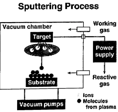
schematicdiagram
of asputtering
systemis
shownin Figure 2.1.
Sputtering
Process
Vacuumpumps
Reactive
gas
ions Molecules
[image:38.522.165.361.428.613.2]fromplasma
Figure 2.1:
Schematicof asputteringprocess2.1.1
D.C.
MAGNETRON
SPUTTERING
In
d.c.
magnetronsputtering,
electricfield is
theresult of ad.c.
voltage, wherethe target
is
cathode and the substrateholder
is
made anode.The
target and substrate areseparated
by
5
to10
cmbut
most of the volumebetween
the target and substrateis
occupiedby
theelectrically
neutral plasma.Visually
the plasma appears as a glowdischarge
with adark
space overthecathode.The
applied potentialis
concentratedin
thedark
spacegiving
risetoalarge
electricfield.
Current flow is
theresultofAr
+ions from
plasma to the target and electrons
from
plasma to the substrate.Electrons
cause thesubstrate to
heat up
whenthey
impact it. To
preventthis,
amagneticfield is
appliedin
such away
as toconfine the electrons to thevicinity
ofthe target.This
variation tothestandard
sputtering
arrangementis
called magnetron sputtering.A
second gasmay be
intentionally
mixed with the argon so that thedeposited
materialis
a compound ofthe targetmaterial andthesecond gas.This
is
called reactive sputtering.2.1.2
R.F. MAGNETRON SPUTTERING
When
anelectrically
insulating
materialis
used as a targetfor sputtering in
a standardd.c.
arrangement, positive charge accumulates onits
surface and the sputteryield
decreases
to zero.This
canbe
overcomeby
applying
an a.c. potential to the targetinstead
of ad.c.
potential.A
magneticfield is
also applied asin
the case ofd.c.
sputtering.
As
the potential alternates, the electrodes reverse their cathode-anode rolesevery half
cycle and thereis
adark
space over each electrode.The
frequency
of theoscillations must
be high
enoughtopreventany
charge accumulationduring
thatpart of a cycletheelectrode serves as thecathode.The
Federal CommunicationsCommission has
allocated ther.f.
frequency
range of10
to20 MHz for
industrial,
scientific, and medical applications andmost r.f. sputteringtoolsoperate at13.6 MHz. RF sputtering is
preferredto
d.c. sputtering because
ofits
versatilityin
depositing
conducting, semiconducting
aswell as
insulating
materials.2.2
HYSTERESIS BEHAVIOR DURING SPUTTERING
During
reactivesputtering,
a reactivegas,
usually
N2
or02
is
added to the usualAr
sputtering
plasmatodep