Rochester Institute of Technology
RIT Scholar Works
Theses
Thesis/Dissertation Collections
9-1-2005
A Piecewise Linear Approximation D/A Converter
for Small Format LCD Applications
Mark Reisiger
Follow this and additional works at:
http://scholarworks.rit.edu/theses
This Thesis is brought to you for free and open access by the Thesis/Dissertation Collections at RIT Scholar Works. It has been accepted for inclusion
in Theses by an authorized administrator of RIT Scholar Works. For more information, please contact
Recommended Citation
Thesis Release Permission Form
Rochester Institute of Technology
Kate Gleason College of Engineering
A Piecewise Linear Approximation D/A Converter for Small
Format LCD Applications
I, Mark Reisiger hereby grant the permission of the Wallace Library of the
Rochester Institute of Technology to reproduce my thesis in whole or in part. Any
~eproduction
will not be for commercial use or profit.
Author: _ _ _ _ _ _ _ _ _
_
Mark Reisiger
5---Table
of
Contents
Table
ofContents
2
List
ofFigures
3
1.0
Introduction
4
2.0
System Design Considerations
4
2.1
Liquid Crystal Behavior
5
2.2
LCD
panelarchitecture8
2.3
Low-Temperature
Polysilicon
10
2.4
Continuous Grain Silicon
12
2.5
Timing
andDrive Requirements
14
3.0
D/A
Architecture Selection
17
3.1
Piecewise
Linear Approximation
Method
18
3.2
Piecewise
Linear
System Implementation
22
4.0
Architecture
Implementation
Analysis
24
4.1
D/A
core24
4.2
Sample
andHold
28
4.3
Output
Driver
31
5.0
Proof
ofConcept Design
33
5.1
Differential Amplifier
33
5.2
Output Amplifier
51
5.3
Amplifier Simulation
Results
53
5.4
System
Design
59
5.4
Linear
D/A
Comparison
63
5.5
Physical Implementation
66
6.0
Design
Test
68
7.0
Conclusion
70
8.0
Future
Work
71
9.0
Acknowledgments
71
10.0
Appendices
72
List
of
Figures
Figure 1
-Twisted Nematic LCD Panel
6
Figure 2
-LCD
Transmissivity
vs.Applied Voltage
7
Figure 3
-TFT
LCD Pixel Structure
9
Figure 4
-LTPS Panel Architecture
1
1
Figure
5
-CGS Panel Architecture
13
Figure 6
-Gamma Correction System
14
Figure
7
-LCD Transfer Function
15
Figure 8
-Piecewise Linear
Approximation
19
Figure 9
-(a)
Sample Curve
(b)
Approximation
21
Figure 10
-Sample Curve
Approximation Error
21
Figure
1 1
-System
Block Diagram
24
Figure
12
-D/A
Architecture
28
Figure
13
-Vref
Sample
andHold Architecture
30
Figure
14
-Output Amplifier Block Diagram
32
Figure 15
-PseudoDifferential Amplifier
37
Figure
16
-Pseudo-Differntial Pair
with
Reduced
VT
Sensitivity
39
Figure
17
-CMFB Schematic
43
Figure
18
-FunctionalDiagram
ofthe
Proposed
Amplifier
45
Figure
19
-Input
Balancing
Stage
46
Figure 20
-Dynamically
Biased Amplifier
48
Figure
21
-Output
Amplifier
52
Figure
22
-FD Amplifier
Frequency
Response
54
Figure 23
-SE Amplifier
Frequency
Response
55
Figure
24
-FD& SE
Amplifier
Step
Response
57
Figure
25
-Dynamic
Current
Efficiency
58
Figure 26
-Performance Comparison
Table
58
Figure
27
-Full
Scale Sample & Hold Operation
60
Figure
28
-D/A
Core
withSample &
Hold
Operation
61
Figure
29
-D/A
Core
with
Output
Amplifier
Hold Operation
62
Figure
30
-Ouput Amplifer
Hold
and
Drive
Operation
63
Figure 31
-9-bit
D/A Core Operation
65
Figure 32
-Test
Chip
Layout
67
Figure
33
-Clock Generator
Schematic
72
Figure
34
-Non-Overlapping
Clock Schematic
73
Figure
35
-6-bit
D/A
Top
Schematic
74
Figure
36
-6-bit D/A Core
Schematic
75
Figure 37
-9-bit
D/A
Top
Schematic
76
Figure
38
-VREf
Sample
andHold Schematic
77
Figure
39
-Output Driver Schematic
78
Figure
40
-PTAT
Bias
Generator
Schematic
79
Figure 41
-FD
Amplifier
(Left
Side)
Schematic
80
Figure
42
-FD
Amplifier
(Right
Side)
Schematic
81
Figure 43
-SE
Amplifier
Schematic
1.0
Introduction
Low
power operationis
adriving
requirementfor
the
advancement of portableconsumer electronics.
As
products get smaller andhave
morefunctionality
the
device
integration
requirements gettighter.
This
is
certainly
true
of smallformat LCD
applications
like PDAs
and cell phones.Recent
advancesin
LCD
technology
have
allowed
for
advancedcircuitry
to
be built
onthe
glass.This
allowsfor
the
uniqueopportunity
to
integrate
the
LCD
columndriver
with othercircuitry
ratherthan
the
traditional
flip
chip mounting
onthe
glass.The
integration
ofthese
D/A
converters withdigital circuitry
presents a new set ofdesign
considerations.These
considerations allowfor
the
exploration of non-traditional architectures and algorithms.This
work willexplore
these
design
considerationsin detail
and present a novel algorithmfor
conversionas well as a system
implementation
ofthis
algorithm.The
systemimplementation is
compared
to
a standardlinear
converterto
weighthe
relative advantages of each.A
high
performance
dynamically
biased
amplifieris
developed for
usein
the
D/A
converter.This
amplifierhas
ahigh
slew rate whileconsuming
a small amount of quiescent power.2.0
System Design Considerations
In
orderto
appreciate all ofthe
design
considerationsthat
apply
to
the
D/A
converters, the
operation ofLCD
panels mustfirst be
analyzed.While
several newtechnologies
such asLow Temperature
Polysilicon
(LTPS)
andContinuous Grain Silicon
2.1
Liquid Crystal Behavior
Liquid
crystals are molecules with some unique physical properties.These
materials
have
properties which are somewherebetween
those
of solids andliquids.
Liquid
crystals cantake
on severaldifferent
types
ofphases;
the
nematicphaseis
usefulfor
display
technologies.
In
the
nematic phase all ofthe
crystalshave
atendency
to
orient
themselves
in
the
samedirection
asthe
molecules nextto them.
Liquid
crystalsalso possess
the
property
ofbirefringence.
Birefringence
meansthat
a materialhas
two
different indices
of refraction.The way
in
whichlight is
refracteddepends
onits
orientation as
it
passesthrough the
material.Liquid
crystals are also adielectric
andthey
are polar molecules so
that
their
orientation canbe
controlled with an electricfield.
All
ofthese
properties canbe
manipulatedto
produce anelectrically
controlledoptical
filter,
whichis
the
basis
of anLCD.
The
twisted
nematic architectureis
the
mostcommon
way
to
manufacture aLCD
panel.Since
the
moleculesin
the
nematic phasetend to
alignthemselves to their surroundings, their
orientation canbe
controlled.Figure
1
showsthis
structure.Liquid
crystals are sandwichedbetween
two
layers
ofglass.Each
layer
of glassis
coatedin
atransparent
conductive material such asIndium
Tin
Oxide.
The
inside
ofthe
glassis
coated with a polymerthat
has
been brushed in
onedirection.
The
nematicliquid
crystalstend to
alignthemselves
withthis
polymer.The
twisted
nematic structure gets
its
namebecause
the
polymers ofthe
top
andbottom
panels arebrushed
orthogonally
to
each other.The liquid
crystalsnaturally follow
this
90 degree
This
structure produced someinteresting
optical properties.The
gradualtwist
in
the
liquid
crystals causesany light
passedthrough the
panelto
be
refractedresulting in
a90 degree
shiftin
polarization.In
orderto
completethe
panel,
external polarizers areplaced on
the
outsidesofthe
panel.These
polarizersare orientedin
the
samedirection
asthe
brushed
polymer ontheir
respective panels.At
steady
state,
this
allowslight
to
passthough the
panel sincethe
liquid
crystals performthe
necessary
refractionto
allowlight
to
passthrough
orthogonalpolarizers.Figure 1
-Twisted
Nematic LCD Panel
This
behavior
canbe
alteredby
applying
an electricfield between
the
glass platesas show
in
the
righthalf
ofFigure
1
.The
electricfield
acts uponthe
polar moleculescausing
them
to
orientthemselves
in
the
direction
ofthe
field. This force is balanced
by
the
nematicbehavior
ofthe
liquid
crystals.For
low field
strengths,
the
crystalsstay
moreoriented
in
the twisted
nematic structure.At
high
fields,
the
molecular polarizationdominates
the
behavior.
At
these
high
fields,
the
liquid
crystalsdo
not refractthe
incoming
light in
apredicable manner.In
this condition, the
orthogonalpolarizing filters
block any light from passing
though the
panel.At
intermediate field
strengths,
some ofpanel.
These
electricfield
strengths arethe
mostimportant for displays
sincethey
allowfor
the
adjustmentofthe
opticaltransmission
efficiency
ortransmissivity
ofthe
panel.The
transfer
function between
the
electricfield
andthe
transmissivity
ofthe
panelis
animportant
characteristic.Applied
voltage willbe
considered ratherthan
electricfield
sincethe
dielectric
width ofthe
panelis fixed.
Figure 2
showsthe typical
transmissivity
transfer
function
of a panel.At
low drive
voltagesthe
field does
not exertmuch control over
the
liquid
crystals.This
manifestsitself
as adead band
in
the transfer
function
ofapproximately
200
mV.Similarly,
high
voltagesforce
all ofthe
moleculesto
become
aligned, completely
blocking
alllight from
passing.This
canbe
seen asthe
saturation when
the
panelbecomes
overdriven.Another
important
characteristicto
noteis
that
the
transmissivity
does
notdepend
onthe
polarity
ofthe
applied voltage.Practically,
all panels aredriven
withalternating
voltagesto
preventthe
electroplating
ofion impurities
ontothe
glassdue
to
DC bias.
This
is
a major cause of stuckimages.
Figure 2
-LCD
2.2
LCD
panel
architecture
The ability
ofthe
twisted
nematicarchitectureto
modulatethe
light
intensity
mustbe
exploitedto
createdisplays
capable ofproducing images.
Like
otherdisplay
technologies
that
exist,
LCD
panels arebroken down into logical image
cells calledpixels.
These
pixels are composed ofindividual
red,
green,
andblue
cells.By
modulating
the
relative amounts ofthese
colors which areemitted,
the
whole spectrumof coloris
approximated asthe
light is
mixedtogether
in
the
human
eye.Since liquid
crystal panels canonly
modulatelight,
colorfiltering
is
neededto
produce
the
individual
sub-pixels.A
back light
providesthe
complete optical spectrum atthe
rear ofthe
panel.The
liquid
crystals modulatethe
amount oflight
that
passesthrough
the
panel andindividual
colorfilters
are masked onthe
top
ofthe
panelto
select which portions ofthe
spectrum passthrough.
Since
the
individual
colors ofevery
pixel needsto
have independent
control ofthe
transmissivity,
individual
electrodes are needed.A
system
is
neededto
controleach ofthese
sub-pixelsindividually.
The Active Matrix
(AM)
architectureis
usedfor high-resolution displays
which arethe
focus in
this
work.In
this
scheme,
the
individual
sub pixels arebroken down into
a matrix of rows and columns.A
distinguishing
feature
ofthe
active matrixdisplay
is
that
each pixelis
only
driven for
a smallfraction
ofthe total
display
time.
Capacitance
present
in
the
sub pixelholds
the
control voltageuntilit
is
updatedduring
the
nextframe.
Switches
are needed onthe
panelin
orderto
controlthe
addressing
ofthe
sub-pixels.In
the
TFT-LCD,
athin
layer
ofsiliconis deposited
directly
onthe
glass.This
siliconis
used
to
createMOSFETs
which are arrangedin
the
configuration shownin
Figure
3.
Column
mColumn
m+1Column
m+2Rown
Rown+1-R
-r
R
~r
G
_JT_
O
o
o
>;
B
O O O
-Ttl
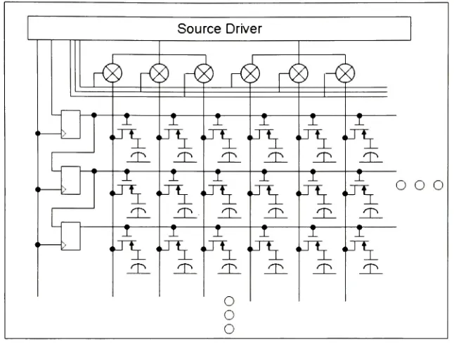
[image:11.520.124.409.142.385.2]I
i
Figure 3
-TFT LCD Pixel Structure
The
sub pixelsin
Figure
3
are addressedin
the
following
manner.A
gatedrive
signal
is
appliedto the
current row.This
turns
onthe
FET
which connectsthe
upperpixel electrode
to
its
column.The
appropriate voltageis
appliedto the
columnlines
by
the
sourcedriver. This
voltage createsthe
field
acrossthe
liquid
crystalsin
that
sub pixelregion.
The bottom
electrode ofthe
panelis
commonto
all ofthe
pixels.The
traditional
TFT-LCD
just described is
typically
an amorphous silicondisplay.
The
siliconthat
is deposited
onthe
glassis
endsup
in
an amorphous state.The
siliconcannot
be
annealedusing
traditional
electronicsprocessing
methodsbecause
the
annealamorphoussilicon suffer
from low
carrier mobility.These
devices
arelarge
andthe
gatedrivers generally
needto
swing between
+10
V
to turn the
device
on and-5V
to turn the
device
off.The devices built in
amorphous silicon areonly
useful as pixel switches.The
poordevice
characteristicsin
amorphous silicon panelsforce
complicatedpackaging
anddrive
solutions.All
ofthe
interconnect
mustbe brought
off ofthe
glasspanel
to the
row and columndrivers.
Typically,
these
drivers
are mounted as aflip-chip
package
due
to the
large
number of connections.The
voltages requiredto
drive
the
gatesare much
higher
than
modern standardCMOS
processes use.This
meansthat the
gatedriver
chips mustbe independent from
the
otherdrivers
andthey
will need an externalDC-DC
converterfor
the
supplies.In
smallformat
displays,
all ofthis
complexity
is
extremely
costly
and prohibitsthe
efficient manufacture ofhigh
resolutiondisplays.
For
example,
a quarterVGA
(320x240)
panel would require960
connections(3
RGB
*320)
to the
sourcedriver
and240
connectionsto the
gatedriver.
2.3
Low-Temperature Polysilicon
Enhancements
in
the
processing
ofLCD
panels reduce some ofthe
complexsystems
integration
problems with standard amorphous silicon.Low-Temperature
Polysilicon
(LTPS)
is
a processthat
has been developed
by
Phillips
to
producetransistors
with
better
performance attributes on glass.A
LPTS
panel starts outlike
an amorphoussilicon panel.
After
the
layer
of siliconis deposited
the
glass panel an excimerlaser is
used
to
annealthe
silicon.The
surface anneal creates polycrystalline silicon whileremaining
below
the
450
C
glasslimit.
Transistors
madefrom
this
polysilicon canBasic
electronics canbe
createddirectly
onthe
LTPS
glass.Typical
panel architecturesare shown
in Figure 4.
The
capacitorsin
this
figure
representthe
capacitance ofthe
individual
pixelelements.Source Driver
[^
^
ft ft
ft
ft
rjb
1-^) |-(g)H&
ft
ft
ft
^EL
<JTL
Ft
JO.
ft
O
o
o
ft
jo.
|J\
ft
J3^ft
^EL
ft
<JTL
ft
o
o
o
[image:13.520.94.417.139.387.2]ft
Figure 4
-LTPS Panel Architecture
In
aLTPS
panel, the
gatedriver has
been
eliminated.A
series of shift registersare connected
to the
gates ofthe
individual
pixels.These
shift registers are clocked atthe
line
rate ofthe
panel.A
starttoken
is driven into
the
first line
register atthe
beginning
ofthe
frame.
This
token
gets clockeddown
the
panel, automatically
selecting
the
properrow.
In
additionto
the
elimination ofthe
gatedriver,
the
interconnect
requirements ofthe
sourcedriver have been
reduced.It
is
possibleto
createlow
ratio(3:1)
multiplexersin
the
source columns.The
amount of external connectionsthat
are neededhave been
reduced
by
afactor
ofthree.
Since LPTS
panelstake
extraprocessing
stepsto
make,
they
the
elimination ofthe
rowdrivers
and other support circuitry.LTPS
panels offer realfinancial
benefits for
smallformat displays.
2.4
Continuous Grain Silicon
Further improvements have been
made withContinuous Grain Silicon
(CGS)
LCD
panels.This
proprietary
process whichhas been
pioneeredby
Sharp,
claimsto
offer carrier
mobility
of300
cm2/Vs.
This
figure is 600
times
faster
than
amorphoussilicon and
three times
faster
than
LTPS.
The
improvements in
transistors
allowfor
evengreater
multiplexing
ratios of80: 1
.These
multiplexers can nowbe
controlledby
on-glass
addressing
electronics; this
meansthat
a similartoken
passing
structureis
usedfor
the
sourcedrivers
asis
usedfor
the
gatedrivers.
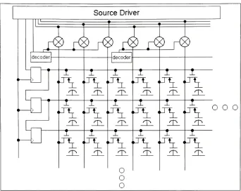
Figure 5
shows atypical
CGS
panelSource Driver
> > decoderlp
c=;
"T:
_^d_Ft
.j^
^n.
pi
PL
ft
Si.
Ft
decoderFt
Ft
Ft
O
O
o
r
r<$>Ft
Ft
j3^
Ti
ft
Jt
Ft
-5r~ft
^P
~5r~ft
_ELTl
JIL
[image:15.520.98.440.57.329.2]o
o o
Figure 5
-CGS
Panel Architecture
The
benefits
ofCGS
displays
canbe
readily
seenfrom
a systemdesign
perspective.
The 80:1
multiplexer ratios allow aQVGA
display
to
be
driven
withfour
RGB
(12
total)
sourcedrivers.
The
panel also needsjust
afew
control signals.This
means
that
a simpleflex
tape
couldbe
usedto
routeinterconnect
and noflip-chip
packaging
is
required.Since
the
sourcedrivers
are nolonger
requiredto
be
isolated,
interesting
packaging
possibilities exist.A
system on achip
approach encouragesintegrating
all ofthe
sourcedriver D/A
converters andoutputbuffers in
a singlechip
with2.5
Timing
and
Drive
Requirements
The
practicaldrive
requirements placed uponthe
sourcedrivers
mustbe
taken
into
account.The first
requirementis
the
effective resolutionthat
LCD
panels support.Generally
a panel can support64 levels
oftransmissivity.
The
D/A
converter needs morethan
6-bits
of precisiondue
to the
nonlinearity
ofthe transfer
characteristic.The
intrinsic
nonlinearity
ofthe
liquid
crystals wasdiscussed in Section 2.1.
However,
this
is
notthe
only nonlinearity in
the
system.Like
all other videosystems,
gamma correctionis
needed
in LCD
panels.This
curvature correctionis
neededto
linearize
the
response ofboth
the
human
eye andthe
videoencoding
method.Figure 6
shows a systemlevel
diagram
withthe
gamma coefficients at each stage.A
+Video Source
LCD Panel
Human Eye
(X)0.45
A0.45
(x)25
A1.125
? (X)088 ?A
Figure
6
-Gamma Correction
System
The
sourcedependency
ofthe
gamma correction showsthe
needfor
anadaptablesystem.
The
LCD drivers
shouldbe
ableto
generateany
possible curvefor
the
requiredsystem.
In
orderto
do
this the
worstcasedrive
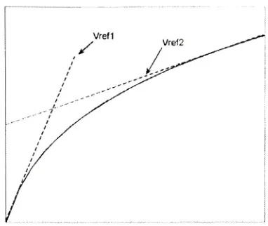
voltage mustbe found. Figure 7
shows aLCD
transfer
curvein
which gamma correctionhas
been
applied.The
panelbetween
single steps oftransmissivity
is 18
mV.This step
represents0.36%
ofthe
5 V
full
scale.Rounding
up
to the
nearestbit
implies
that
a9-bit
effective resolutionlinear
converter
is
needed.50
o
I
3010
-1 0 1
Vapplied
Figure
7
-LCD
Transfer
Function
The
dynamic
requirements ofthe
LCD
paneldrive
must alsobe
considered.The
first
specificationis
the
maximum conversiontime
for
each pixel.This
is
adifficult
requirement
to
determine
sinceit is
panel-specific.The
horizontal
and verticalblanking
periods change
slightly
between
manufactures.Worst
case quantities are consideredto
determine
anapproximatepixeltime.
The
line
rateis
calculated asfollows:
line
rate=1
1
frale(Active
_lines
+
Blanking
_
lines)
60(240
+7)
=
61.5/js
The
assumptions madein
(1)
are asfollows:
The QVGA
display
is
refreshedusing 60 Hz
video andthe
display
requires7
lines
of videoduring
the
vertical refreshperiod.
The
pixeltime
may
nowbe determined from
the
line
rate.Again
assumptionsabout
the
horizontal
blanking
period are made.A
worstcaseblanking
interval
of3
usis
used.
The
systemis
also assumedto
have four
D/A
converters per color.. ,
(line
rate-Blanktime)
(67.
5
us-3us)
n_, ... PIXSI-^
=
fColumns/
"=
320/
=
85
(2)
/UDACs
/4
Each D/A
mustbe
ableto
settleto
9-bit
precisionin 805
ns orhave
a conversion rate of1.3MS/S.
The
LCD
panel presents aload
that
looks
primarily
capacitiveto the
sourcedriver.
Each
individual
pixelhas
some small amount ofcapacitance,
plus all ofthe
metallization on
the
glass andin
the
flex
cable presents additional parasitic capacitance.The
multiplexer and pixel switches will present some on-resistance andthe
interconnect
will
have
some small sheetresistance.These
parasiticsaredifficult
to
model andthe
load
that
they
present will changebased
uponthe
physical pixel whichis
addressed.A
load
of3.0
D/A
Architecture
Selection
The D/A
architecture oftraditional
columndrivers
is
fairly
straightforward.
These 9-bit
converters areimplemented
with aresistorstring
architecture.This
structureoffersseveral advantages such as
simplicity in implementation
andguaranteedmonotonicbehavior.
Simple
polysilicon resistors match well enoughto
be
usedto
achievethe
required
9-bit
precision.This
meansthat
a standardCMOS
processmay
be
used.The
major
limitation
ofthe
R-string
D/A
is
the
power-speedtradeoff.
The
majortime
constant of
the
systemis
formed
by
the
currentlimited
charging
ofthe
parasiticcapacitances of
the
amplifier andinterconnect.
Assuming
that
these
parasiticcapacitances are constant
for
any
givensystem, the
only way
to
makethe
converterfaster
is
to
burn
more powerin
the
R-string.
This
implies
that there
exists some minimumpower consumption
for any
given conversion rate.A
less important limitation
ofthis
architecture
is
that
the
output amplifier offset willlimit
the
channelmatching
ofthe
system.
To
consider alternative architecturesthe
system goals shouldbe
restated.Low
power consumption
is
the
primary
design
objective.Small
die
area andcompatibility
with
digital CMOS
processes are alsoimportant.
In
orderto
meetthese
goals aswitched-capacitor
implementation
is developed.
The
use of switched-capacitors eliminatesthe
need
for
resistorstring bias
current.The
major objective ofthis
investigation
notso muchthe
architectureofthe
D/A,
but
the
method ofproducing
the
LCD
transmissivity
curve.Typically,
a9-bit linear
concept of
using
apiecewiselinear
approximationofthe
curve as a method ofreducing
the
converter performance requirements.3. 1
Piecewise Linear
Approximation Method
The
goal ofthe
piecewiselinear
approximation methodis
to
reducethe
systemrequirements of
producing
a nonlinear curveby
the
brute force
lookup
table
method.In
this
methodthe
precision ofthe
converteris
setby
the
minimumstep
size ofthe
curvethat
is
to
be
reproduced.In
curves withlarge dynamic
ranges, this
approach can resultin
many
unusedbits.
The
core conceptbehind
the
piecewiselinear
approachis
to
break
the
curveup
into
segments.Each
segment canthen
be
constructedusing
alow
precision converter.Figure 8
showsthe
basic
concept.The
solid curveis
the
desired
transfer
function.
The
two
linear
approximations arefitted
tangent to the
desired
curve.This
methodleaves
some residual error as
the
linear
approximationsleave
the
curve neartheir
junction. The
Figure 8
-Piecewise Linear Approximation
If
the
erroris
too great,
anotherlinear
segment canbe inserted between
segments1
and2.
This
process can continue untilthe
absolute errorof each wordis
under somemaximum error
threshold.
This
limit
ofthis
approach occurs whenthe
curveis
sononlinear
that
each word requiresits
ownlinear
approximation.At
this
level
the
technique
degenerates into
the
look-up
table
approach.Therefore
it is
appropriatefor
slightly
nonlinear curves.It
should alsobe
notedthat there
is
roomfor
optimizationin
the
linear
segmentplacement.
Placing
the
segmentstangent to the
curve createsthe
worst possible absoluteerror at
the
transition
points.Most
applications willbenefit from spreading
the
approximation error across all of
the
codes.An
optimized algorithm would use atechnique
such as aleast-squares
regressionline
to
minimizethe
meansquareerrorin any
segment.
This
technique
has further
problems sincethe
length
ofany
single segmentis
entire curve.
The
optimizationofthe
approximationmethodis beyond
the
scope ofthis
work.
A
proof ofconceptalgorithmis developed
to
apply
this
technique to
any
generaltransfer
curve.The
curveis
setalong
withits limits
of precision.This
curveis
then
approximated with a single
segment;
the
end points ofwhich are onthe
limits
ofthe
curve.
The
absolute errorfor
each codeis
calculated.Assuming
that
any
errors areoutside
the
limits
of precision anotherbreak
pointis
added atthe
codewiththe
maximumerror.
New
linear
segments are createdusing
these
additionalbreak
points.The
endpoints of
the
new segments are always placed onthe
desired
curve.After
eachoperation,
the
calculated values are roundedto the
nearestbit
of precision.This
processiterates
until all of
the
errors arebelow
the
presetthreshold.
For
each curvethe
following
information is
generated:The digital
wordboundaries
wherethe
segmentis
valid,
the
gain required
to
generatethe
slope andthe
offset voltage requiredto
alignthe
curve.A
Matlab
simulation was usedto
verify
this technique
for
the
LCD
transfer
curve.The
test
curvein
Figure
9a
is
generated asthe
requiredinverse
curveto
linearize
the
LCD
transmissivity
curvein
Figure
7.
The
limits
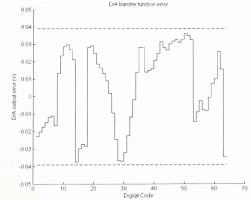
of precision are setto
6-bit
levels for
the
gainand offset coefficients.
The
curve errorlimits
weresetto
lA
LSB
oftransmissivity
atthe
6-bit
level.
Figure 9b
showsthe
curvethat
is
generatedusing
this technique.
The
approximation
is done
with sufficientaccuracy in
twelve
segments.Figure 10
presentsD/Atransferfunction D/Atransferfuncto
10 20 30 40
DigitalCode
10 20 30 40
[image:23.520.133.384.349.549.2]DigitalCode
Figure 9
-(a)
Sample Curve
(b)
Approximation
0 05
0 04
0 03
0 02
D/Atransfer functionerror
rJ\
I
10 20 30 40 50
Digital Code
60 70
3.2
Piecewise Linear System
Implementation
The
piecewiselinear
approximation methodis
a generic processfor creating
nonlinear
transfer
curves.A
specificimplementation
ofthe
architectureis
nowdeveloped.
As
statedin Section 3.0
a switched capacitor approachis
used.The idea
ofproducing
nonlineartransfer
curvesusing
switched capacitor circuitshas been looked
atpreviously
[1],
[2].
There
are several problems withthe
hard-wired
approach.The
first
is
that the
LCD
transfer
curve andthe
required gamma correctionmay
notbe known.
Secondly,
considerable circuit effortis
neededto
generatethe
nonlinearities.For
asystem such as
this
one withtwelve
breakpoints,
the
number of amplifiers andcomparators needed would ruin
any efficiency
that the technique
mighthave
over asingle
9-bit
converter.The
piecewiselinear
technique
developed in
Section 3.1 only
requires afew
components.
In
orderto
generateany
one segment a reference voltage and an offsetvoltage are needed.
The
reference and offset voltages which are usedfor any arbitrary
incoming
word canbe
selecteddigitally
sincethe
break
points were set on codeboundaries.
Thus
the transfer
function
ofthe
systemlooks like
(3)
wheremis
a selectionindex
for
eachbreakpoint
region.Vout
=Vref[m]
N
+Vos[m]
(3)
In
orderto
maximizethe
programmability
ofthis
system,
D/A
converters willbe
curve generation
information
to
be
storeddigitally. This
alsomeansthat the
system mustperform
three
6-bit D/A
conversionsfor
every
output word.To
reducethe
area requirement ofthe
system,
one converteris
usedfor
allthree
conversions.
The
VREF
andVos
voltages willbe
temporarily
maintainedin
sample andhold
circuits.Figure
1 1
showsthe
proposed architecture.The
system operatesin
the
following
manner.A
6-bit
word comesinto
the
digital
controlblock.
A
comparatorcircuit
determines
whichlinear
segmentthe
wordbelongs
to.
The
result ofthis
comparison selects
the
proper conversion codesfor
VREF
andVos
from look
up
tables.
Vref
is
the
first
wordto
be
converted.The
timing
controller selectsthe
fixed
referencevoltage
to
prechargethe
D/A
converter.This
resultis
storedin
the
sample andhold
shown at
the
bottom
ofFigure
1 1
.The
Vos
wordis
the
nextto
be
converted.Once
againthe
timing
controller prechargesthe
D/A
to the
fixed
reference voltage.The
controllerselects
the
offset sample andhold
to
storethe
result.Finally
the
timing
controllerprecharges
the
D/A
withthe
soft reference voltage present onthe
sample andhold.
This
conversion represents
the
first
term
in
equation(3).
The
result ofthis
conversion willbe
referred
to
asVword-
The
resultis
storedin
the
final
sample andhold.
In
orderto
minimize
the
timing
requirementsfor
the
system,
the
D/A
core andthe
outputbuffer
actas a
two
stagepipeline.The
D/A
core converts pixelN+l
whilethe
outputbuffer drives
pixel
N.
The
outputdriver
sumstogether
V0s
andVword
to
form
the
final
word.This
buffer
also providesany scaling
neededfrom
the
core and providesthe
currentdrive
Input Code
Input
Comparator,
Vref
LUT,
Vos
LUT,
Sequencer
6-bit
D/A
S/H
S/H
I
I
S/H
V
REFvr
Figure
11
-System
Block
Diagram
4.0
Architecture Implementation Analysis
Many
ofthe
systemrequirementshave been
analyzedin Sections
2
& 3. These
requirementsare setby
the
physical properties of aLCD
panel andby
the
needs ofthe
piecewiselinear
approximation method.All
ofthese
systemlevel
requirementswillbe
broken down into
specificsectionsin
orderto
accurately
define
the
performance characteristics of eachblock.
4.1
D/A
core
The
D/A
core mustbe
the
highest performing
component ofthe
overall system.This
converteris
requiredto
generatethe reference, offset,
and word voltagesduring
asingle pixel cycle.
The decision
to
use a switched capacitor approachhas already been
made,
but
there
are severaltypes
of converters whichfall
withinthis
domain.
The
benefits
of each architecture willbe
analyzed;
with a particularfocus
on conversionArchitectures
that
usethe
charge redistribution principle[3]
offerlow
poweroperationsince
they
only
utilize a singledifferential
amplifier.Charge
redistributionis
aprecharge-evaluate architecture so
the
amplifier mustbe
capable ofsettling
twice
in
asingle conversion cycle.
This
architecture relies on abit
dependent
numberof capacitors.For
the
6-bit
converter,
64
unit cells of capacitance are neededin
the
feedback
path.Likewise,
63
individual
capacitors are neededin
the
input
stage.These
127
capacitorsneed
to
be
matchedto
greaterthan
9-bit
precision.This
resolutionimplies
that
matching
better
than
0.19% is
needed.The matching
requirementsin
[4],
[5]
place alimit
to
the
minimum area and
therefore
the
minimum capacitance ofthese
unit cells.These
minimum sized capacitors place additional
drive
requirements onthe
differential
amplifier.
This
amplifier mustbe
capable ofsettling
these
64
unit capacitorsin
the
feedback
path.Cyclic
converter architectures offer severalimprovements
when comparedto
charge redistribution converters
[6],
[7]
and[8].
These
converters operateserially;
they
convert a single
bit
at atime
andhold
the
incremental
result.This
meansthey
rely
on apair of matched capacitors.
This
considerably
reducesthe
matching complexity
ofthe
system.
The die
area usedby
a cyclic converteris
muchless
than
a charge redistributionconverter
because
ofthe
reduction of capacitors.The
slew rate requirements ofthe
amplifier are reduced
for
the
same reason.Unfortunately,
the
settling
time
requirementsof
the
amplifier aredrastically
increased.
Due
to the
serial nature ofthe
architecture2n+l
clock cycles are neededfor
an-bit converter.This
requirementmakesit unlikely
to
use a singleD/A
for
allthree
words as shownin
Figure
1
1
.Since
the
pixeltime
is
61
nsfor
each6-bit
conversion.Anything
faster
than this
would seeminfeasible for
alow-power
design.
Pipeline
converters combinethe
benefits
ofboth
ofthe
previous architectures.This
architectureis
an extension ofthe
cyclic architecture andis
typically
usedin
A/D
converters
to
increase
their
conversion speed[9].
This
architecture places one cyclicconverter
for
eachbit.
These
singlebit
converters passtheir
incremental
resultsto the
nextconverter.
Pipeline
converters still offerthe
advantages ofthe
small areaof a cyclicconverterwhile
eliminating
the
needto
settle2n+l
times
during
a pixel.However
these
benefits
are counteractedby
the
needto
have
n amplifiers.The
large
number ofamplifiers
does
notlend itself
wellto
low
powerdesigns.
Since
the
primary
goal ofthis
systemis
low-power
operation,
the
chargeredistribution architecture
is
chosenfor its lenient
settling
time
requirements and use of asingle amplifier.
Several
refinements needto
be
madeto the
basic
architecturein
orderto
fit
this
application.First
ofall, this
design is intended
to
operate within adigital
environment.
This
meansthat
it
musthave
good rejection of all ofthe
switching
noisepresent on
the
chip.Due
to the
large
number of capacitorsthat
areneeded,
the
smallestvalue
that
canbe
matched willbe
used.Small
capacitors manifest chargeinjection
errorsas
large
voltage errors.In
an attemptto
reduceboth
ofthese
effects afully
differential
architecture will
be
used.The
othernon-ideality
which mustbe
contendedwithis
offsetvoltage
in
MOS
amplifiers.On
a5
V
powersupply,
9-bit
precisionimplies
approximately
10
mV as aLSB
voltage.The
offset voltagefor
untrimmed amplifiersauto-zeroing
approachis
taken.
The
gain amplifierin
[10]
samplesthe
amplifieroffsetin
the
precharge clock phaseandsubtracts
it
during
the
conversion phase.The
completeD/A
architectureis
shownin
Figure
12.
The
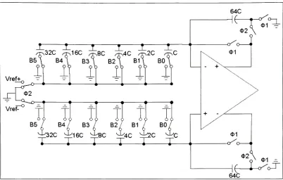
converter operates asfollows.
During
the
precharge phase(Oi),
the
programmable capacitorarray is
chargedto
eitherVrefot
signalground1
depending
onthe
incoming
digital
word.The
amplifieris
placed
in
aunity
gain configuration with noinput
signal exceptfor
the
amplifier's offsetvoltage.
This
voltageis
sampled onthe
feedback
capacitors andthe
capacitor array.During
the
evaluate phase(O2),
the
feedback
capacitoris
placedback in
the
amplifierfeedback loop. The
programmable capacitorarray
is
driven
to
signal ground.This
forces
the
voltage acrossthe
array
to
equalthe
amplifier offset voltage whicheffectively
transfers the
charge ontothe
feedback
capacitor.The
incomplete
chargetransfer
due
to
offset voltage
is
counteractedby
the
offset error sampledduring
the
precharge cycle.64C
02
X
01
--Vref+,
-t
:
I
I
T
T
u
^32C ^16C ^8C ,tMC /^2C ^C
B5A
B4A
B3\
B2
\
B1l
BOA
OD ob ob ob ob ob
02
Vref-
T
r^
r"?
^~?
=~t~
op
op
op
op
op
o<B5
/
B4/
B3
/
B2/
B1
/
BO/
'16C
lJ>8'"O-'/ir*
J-^r
>J>i ,V!32C
^16C
_^_BC_^4Cb^2C
^C
1
i
i
i
i
1
if64C
Figure
12
-D/A Architecture
4.2
Sample
and
Hold
The
sample andhold
circuits are requiredto
storethe
intermediate
voltages usedin
the
construction ofthe
final
word.The
requirementsfor
each sample andhold
areslightly
different.
The
circuitthat
storesVREF
must alsobe
capable ofdriving
asignificant capacitive
load. This
circuit must chargethe
programmablecapacitorarray in
the
D/A
coreduring
the
softVREF
conversioncycle.The
sampleandhold
circuitsfor
V0s
and
Vword
mustsimply
providethe
voltagesto
asumming
junction in
the
output [image:30.520.64.466.58.314.2]The
VREF
sampleandhold
circuithas
many
ofthe
samedrive
requirements asD/A
core.
This
circuithas
a similar capacitiveload
sinceit
willbe
driving
the
programmablecapacitor array.
The settling
time
requirements must alsobe
the
same.All
ofthe
nonidealities
ofthe
system are presenttoo.
Because
ofthese
issues
andto
maximizedesign
reuse
the
samedifferential
gain stage withauto-zeroing
willbe
usedfor
the
sample andhold. Figure
13
showsthis
architecture.The
issue
of amplifier compensationneedsto
be
addressed.
These differential
amplifiers areload
compensated.The
sampleandhold
willhave
varying
capacitiveloads based
uponthe
switch states.The first
variationis based
on
the
incoming
digital
word.The
number ofunitcapacitors charged canvary
between 0
and
63.
The
amplifier alsoonly drives its
ownfeedback
capacitanceduring
the
cycleswhen
the
load is disconnected.
Depending
onthe
specificdesign
ofthe
amplifierit may
Figure
13
-Vref
Sample
andHold
Architecture
The
requirementsfor
the
output sample andhold
circuits are quitedifferent.
Since
these
circuitsonly
needto
drive
their
chargeinto
an amplifier virtual groundthey
can
be
purely
passivedevices.
These
passivedevices have
several unique requirements.The
first
ofthese
issues is
chargeinjection.
This
issue is dealt
within
the
same manneras
before.
Fully
differential
structures andtransmission
gates are utilizedin
orderto
minimize
the
chargeinjection
errors.The
otherissue
withthe
passive sample andhold
circuits
is junction leakage.
The
reversebiased
source anddrain diffusions
willflow
some small amount of current which affects
the
hold accuracy
ofthese
circuits.The
amount of
this
junction leakage is
largely
temperature
dependent
andis
the
biggest
issue
at
high
temperatures.
Both
ofthese
considerations willdefine
the
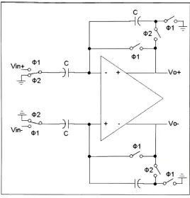
minimum size [image:32.520.131.399.59.339.2]4.3
Output Driver
The
outputdriver is
responsiblefor
severaltasks.
This
amplifier performsthe
summing
action ofVos
andVword-
The
amplifieralso performsthe
differential
to
singleended conversion and signal
scaling
neededto
interface
off chip.In
orderto
accomplishthis task
mirroredSC
gain stages are used.The
negativedifferential input
is
usedto
charge
the
bottom
capacitorarray
whichis driven into
ground2
with a
dummy
feedback
loop
during
the
evaluate phase.This
operation setsthe
amplifierinput
common modevoltage at
the
positiveinput.
The
clocksthat
arelabeled
i
are maskedbased
upontheir
function.
This
precharge clockis
usedto
zerothe
feedback
capacitorsduring
the
beginning
ofthe
pixel cycle.All
ofthe
otherOi
clocks areloading
controlsfrom
the
D/A
core.
Depending
onthe
core conversionstate, this
array
couldbe
chargedwithVword
orVos-
In
addition,
even and odd pixelshave
their
ownholding
capacitors.These
redundant capacitors are not shown
in
Figure 14
for
clarity.These
extra capacitors arenecessary
sincethe
system operates with a pipeline.The D/A
core musthold
wordN+l
while
the
outputdriver is
stillsettling
wordN.
Another
feature
not shownin Figure
14
is
the
V0s
polarity
switch.The
<E>i
maskfor
the
Vos
hold
capacitors queriesthe
state ofinput bit B0.
This
statedetermines
whetherthe
hold
capacitoris
chargedwith standardor
inverted
polarity.The
polarity
switch allows offsetsto
be
subtractedfrom
as well asadded
to
Vword-2
An
important
performancelimitation in
the
outputdriver
needsto
be
mentioned.It
does
notemploy any auto-zeroing circuitry like
the
core amplifiersbecause
ofsettling
time
restrictions.This
meansthat the
random offsetin
this
amplifier willdominate
the
absolute
accuracy
andthe
channelmatching
ofthe
system.V1N+^
V,rr-01
5c
02
02
\
\01
44
01
5C
02
02
\
\01
11
01
5C
02
02
\
\01
11
01
"
5C
02
02
\
\01
11
02
2C
02
01
\ \
01
11
02
2C
02
01
\
\01
11
[image:34.520.68.464.237.542.2]Vn
5.0
Proof
of
Concept
Design
The
systemlevel design
ofthe
piecewiselinear D/A
converter wasdescribed in
Section 4.
This
establishedthe
performance criteriafor
each ofthe
systemcomponents.Detailed
componentdesign
and simulation willbe described in
this
section.The
physicalimplementation
of all ofthe
circuitry
will alsobe included.
The
fabrication
costs ofthis
proof of conceptdesign
were supportedby
aresearchgrant
though the
MOSIS Educational Program.
In
orderto
provide a realistictest
chip
the
TSMC035P2
processhas been
selected.This
0.35
urn processis
the
smallestfeature
size process
that
offersthe
5 V
supportthat
is
neededto
directly
drive
the
LCD
panel.The 0.35
(amtransistors
offer enough performancethat
they
couldbe
utilizedin
the
digital
controller which wouldbe integrated
withthis
design.
TSMC035P2
is
adual poly
process which
is
necessary
for
precision capacitordesigns.
All
simulations wereperformed
using
the
Cadence Spectre
simulator as part ofthe
Cadence design
suite.5. 1
Differential Amplifier
The fundamental
componentin
this
design is
the
differential
amplifier.This
amplifier
is
burdened
withfast
settling
time
requirements whilemaintaining low
poweroperation.
The
amplifier must alsohave
relatively
high
gainfor
converteraccuracy
andit
This
amplifiermusthave
a certainlevel
ofstatic performancein
orderto
meetthe
accuracy
requirementsofthe
system.Since
the
systemis
requiredto
have 9 bit
accuracy
this
amplifiermusthave
muchbetter
precisionthan that.
In
orderto
get an estimate ofthe
required
gain,
DC
errors willbe
allowedto
be % LSB.
The
gain requirementsfor
the
worst case
unity
gain conversion are calculatedfrom
the
standardfeedback
transfer
function
equationin (4).
F
= - =1
- =0.999517
X
+A/3
}_
2
9
4
(4)
F
0.999517
n/(_rr,n
A
= = =2047
=66dB
l-F/3
1-1
-0.999517In
orderto
understandthe
currentdrive
andfrequency
response requirements ofthe
amplifierthe
minimum sized capacitor mustbe
determined.
The
matching
capabilities of
this
process were obtainedfrom
the
recommendations of a successfulcommercial
10-bit
switched-capacitordesign3. The
recommendations statethat there
wasno yield
loss due
to
capacitormatching
when1 1
u.mby
1 1
umtop
plates were used andthe
corners were chamferedto
maximizethe
areato
perimeter ratio.The
unit cellis
derived
in (5).
Cunit
1 l/jm
1 \/jm
- 4(l//m
l/um)
%10aF/
2=103.5^F(5)
The TSMC035P2
processdoes
nothave
athin
oxidebetween
the
two
polysiliconlayers
which resultsin
the
small sheet capacitance value.Regardless,
the
D/A
coreamplifier
in Figure
12
has 64
unit cellsin its feedback
pathresulting
in
a6.6
pFload
plusany
capacitancepresentin
the
sampleandhold
circuitsthat
it drives.
The load
capacitance willcertainly
be
the
primary
pole ofthe
amplifier.The
bandwidth
requirements ofthe
system willdetermine
the
requirementsfor
the
outputdriver. In
orderto
get a rough estimate ofthe
bandwidth,
single polesettling
behavior is
assumed.
The
amplifier will needto
settleto
lA LSB
(0.048%)
ofthe
final
valuein
133
ns.The
requiredbandwidth assuming
alinear
responseis
calculated asfollows.
V
=1
-e
A
=
t/
-133
ns/
-17 ,T /-
ln(0.000488
)
~
/7.6
" s(6)
GBW
=~^=9MHz2
TITThis bandwidth
estimateis
very
liberal
sinceit does
not accountfor
multiplepolesettling behavior
or nonlinear effectslike
slew ratelimitations.
The
slew rate requirement ofthe
amplifieris
neededto
determine
the
amplifierbias.
The
slew rateis
estimatedin
the
following
manner.The
worstcaseswing
willbe
approximately
2 V
internally.
The
assumptionis
madethat the
amplifier will not slewfor
more
than
10%
ofthe
settling
time.
This
implies
that
a slew rate of150 V/us is
needed.These large load
currents eliminateClass
A
amplifiers as an option.In
orderto
achievea
D/A
powerconsumptionof severalhundred
microwatts much smaller quiescentcurrentconsumption
is
needed.A
power consumption goal of100
uW per amplifierhas
been
set.The internal
amplifiers will usethe
3.3
V
power suppliesin
orderto
keep
powerconsumption
down
andto
utilizethe thin
gate oxidedevices. This
meansthat this
amplifier must work with
30
uA ofbias
current.To
achievethis,
efficient classAB
structuresare needed with active-to-idlecurrent ratios of more
than thirty-three.
Traditional
classAB
structures are notlikely
to
workin
this
application.These
are
generally
output stages which are added onto a core amplifier.Most
ofthe
amplifiergain
is
createdbefore
these
output stages andthis
large
gain places adominant
pole atthe
internal
node.This
meansthat the
pole created withthe
load
capacitance would needto
be
pushed wellbeyond
the
gainbandwidth.
A
large
amount ofbias
currentis
neededto
create a
low impedance
output node.Assuming
that the
output stageis
a sourcefollower,
the
driving
impedance
is
approximately 1/gm.
To
placethe
secondary
pole at50 MHz
where
it
would contribute10
degrees
of phase shift would require atransconductance
of2.2
mS.Using
moderatesizetransistors
of50
um/ 350
nm and withk'
for NMOS
of97
U.A/V2;
1
80
uA ofbias
currentis
neededto
achievethis
outputimpedance.
Alternative
Class AB
structures are neededthat
will allowthe
load
to
be
the
primary
pole and ahigh
impedance
gain node.Dynamic
Biasing (DB)
is
one solutionto
this
problem.A
dynamically
biased
amplifierworks
by
changing
the
bias
current ofits
output stage as afunction
ofthe
input
signal.
This
is
typically
done
with atraditional
OTA. The
bias
currentis
changedunderimpedances
for
goodDC
gain.Dynamic
biasing
is
typically
accomplished with atransient
detector
which adjuststhe tail
currentonthe
input
pair.This
technique
createsweak positive
feedback in
the
amplifier.Besides
the
stability
concerns,
the
extracircuitry
typically
consumesa gooddeal
of currentto
maintainahigh bandwidth.
Pseudo-Differential
(PD)
amplifiers offerthe
potentialto
be
usedfor dynamic
biasing.
These
circuits areusually
employedin
low-voltage
applications wherehead
room can't
be
spared on atail
current source[11],
[12].
Pseudo-differential
pairs are ofinterest because
they
do
not saturatelike
true
differential
pairs.The
intrinsic
square-lawbehavior
of aMOSFET
canbe
usedto
providethe
amplifierbias
andoptimizegm.Figure 15
showsthe
schematic ofthe
basic
dynamically
biased
PD
amplifier.Under
small signal andidle
conditionsthe
bias
currentis
setby
the
gatedrive
onthe
input
pairMl.
Signals
appliedto the
input
are mirroredto the
output stageformed
by
M3
and
M4.
Transistors M5
andM6
ideally
create symmetric gatedrive
signalfor
the
NMOS
devices
sothat the
n-channel and p-channeldevices
aredriven
equally.Gain
is
createddue
to the
high
channelimpedance
ofthese transistors.
The
gain ofthis
amplifieris
approximately gmi(ro5\
\ro3)
assuming
that the
mirror ratios are1
:1
.%
M2aikJ HiM2bM5a|+J
M3b,
M1a
\J
M3h\J
M3a,tJ
M5b
M1b
|_J IVHU,
JH
-"lM4a
hLh
r
H
<ne
r\
M4b
M6b
The
large
signal operationis
asfollows:
The
signalstep is
assumedto
be larger
than the
quiescent gate overdrive onthe
input
pair.The
input step is
also symmetricabout
the
DC
gatedrive
voltage.This step
turns
Mlb
off sincethe
gatedrive is
nowbelow
the threshold
voltage.Without
supply
currentthe
6-side
mirrors shutdown
andthe
output mirrorsbecome high impedance.
Transistor
Mia
sinks much morecurrent,
ideally following
square-lawbehavior.
This
currentis
mirroredthroughout the
a-sidetransistors
to the
outputb