High-performance GaAs/AlAs superlattice electronic devices in oscillators at
frequencies 100–320 GHz
Heribert Eisele, Lianhe Li, and Edmund H. Linfield
Citation: Appl. Phys. Lett.112, 172103 (2018); doi: 10.1063/1.5020265 View online: https://doi.org/10.1063/1.5020265
View Table of Contents: http://aip.scitation.org/toc/apl/112/17
Published by the American Institute of Physics
Articles you may be interested in
Effect of film thickness on the ferroelectric and dielectric properties of low-temperature (400 °C) Hf0.5Zr0.5O2 films
Applied Physics Letters 112, 172902 (2018); 10.1063/1.5026715
Demonstration of high mobility and quantum transport in modulation-doped β-(AlxGa1-x)2O3/Ga2O3 heterostructures
Applied Physics Letters 112, 173502 (2018); 10.1063/1.5025704
Bandgap opening in hydrogenated germanene
Applied Physics Letters 112, 171607 (2018); 10.1063/1.5026745
Experimental demonstration of the optical Helmholtz resonance
Applied Physics Letters 112, 171110 (2018); 10.1063/1.5028256
Mid-infrared GaSb-based resonant tunneling diode photodetectors for gas sensing applications
Applied Physics Letters 112, 161107 (2018); 10.1063/1.5025531
Correlation between dislocations and leakage current of p-n diodes on a free-standing GaN substrate
High-performance GaAs/AlAs superlattice electronic devices in oscillators at
frequencies 100–320 GHz
HeribertEisele,a)LianheLi,and Edmund H.Linfield
Pollard Institute, School of Electronic and Electrical Engineering, University of Leeds, Leeds LS2 9JT, United Kingdom
(Received 21 December 2017; accepted 4 April 2018; published online 27 April 2018)
Negative differential resistance devices were fabricated from two epitaxial wafers with very similar GaAs/AlAs superlattices and evaluated in resonant-cap full-height waveguide cavities. These devices yielded output powers in the fundamental mode between 105 GHz and 175 GHz, with 14 mW generated at 127.1 GHz and 9.2 mW at 133.2 GHz. The output power of 4.2 mW recorded at 145.3 GHz constitutes a 50-fold improvement over previous results in the fundamental mode. The highest confirmed fundamental-mode oscillation frequency was 175.1 GHz. In a second-harmonic mode, the best devices yielded 0.92 mW at 249.6 GHz, 0.7 mW at 253.4 GHz, 0.61 mW at 272.0 GHz, and 0.54 mW at 280.7 GHz. These powers exceed those extracted previ-ously from higher harmonic modes by orders of magnitude. The power of 0.92 mW constitutes an improvement by 77% around 250 GHz. The second-harmonic frequency of 317.4 GHz is the high-est to date for superlattice electronic devices and shows an increase by 25% over previous results.
VC 2018 Author(s). All article content, except where otherwise noted, is licensed under a Creative
Commons Attribution (CC BY) license (http://creativecommons.org/licenses/by/4.0/).
https://doi.org/10.1063/1.5020265
In their seminal paper of 1970, Esaki and Tsu proposed that semiconductor superlattices (SLs) could be used in devi-ces with “virtually no frequency limitation” since Bragg reflection of electrons gives rise to energy minibands and regions of negative differential velocity in velocity-electric field characteristics.1 At sufficiently high electric fields across such a doped SL electronic device (SLED), traveling domains may form2 and, similar to traveling domains in Gunn devices, cause a negative differential resistance (NDR) between the device terminals. When a SLED of sufficiently high NDR is connected to a suitable resonant RF circuit, RF output power is generated at the resonance frequency.
SLEDs have attracted much attention since the 1990s because the underlying physical process, the Bloch effect, has relevant relaxation time constants that are much shorter than those of the transferred-electron effect in, for example, GaAs Gunn devices.3,4 Therefore, SLEDs have the strong potential of filling the need for compact, reliable, and effi-cient sources of RF radiation with high spectral purity. Such fundamental sources are a prerequisite for many emerging system applications at terahertz frequencies, e.g., ultra-high speed wireless communications, material analysis, imaging, chemical and biological sensing, and space exploration.5
SLEDs with sufficiently wide minibands in the GaAs/ AlAs and InGaAs/InAlAs material systems have already been demonstrated as millimeter-wave oscillators in both the fun-damental and higher harmonic modes,3,4,6–10 As examples, RF output powers of more than 80 mW and dc-to-RF conver-sion efficiencies up to 5.1% were achieved in the fundamental mode around 63 GHz mainly by improving thermal manage-ment using substrateless devices,8 and fundamental-mode
operation up to 155.1 GHz (with an RF output power of 1.1 mW) was been observed.10
In this work, two very similar SL structures were grown by molecular beam epitaxy. TableIlists their structural prop-erties and estimated miniband widths.11In both wafers, and as in previous wafers,8,9the SLs were sandwiched between graded transition layers on both sides,12 and a 0.5-lm-thick Al0.55Ga0.45As layer was grown between the substrate and the
SLED layers to allow for complete substrate removal during device fabrication.8,9,13 For a direct comparison, this table also includes the structure data of Wafer 3 that was evaluated previously9 but has since yielded much improved second-harmonic output powers above 220 GHz.
Device fabrication followed the same process steps described in Ref.9, but somewhat smaller SLEDs, with nomi-nal diameters of 15–35lm, were selected for packaging and RF testing. SLEDs were mounted in the same type of package that has been employed previously in the evaluation of differ-ent types of NDR devices in the GaAs and InP material systems,13–17including SLEDs.8–10All SLEDs from Wafers 1 and 2 were first evaluated in the fundamental mode in a resonant-cap full-height WR-6 waveguide cavity. A subset of these SLEDs was then evaluated at fundamental-mode fre-quencies of 160–175 GHz in a resonant-cap full-height WR-5 waveguide cavity. To confirm fundamental-mode operation, the mechanical tuning range, i.e., oscillation frequency vs. back short position, was first determined. For SLEDs with oscillation frequencies up to 160 GHz, second-harmonic power extraction was then measured. Figure1shows the waveguide configuration for this method where a WR-3 waveguide, which cuts off all signals at frequencies below 174 GHz, is connected to the WR-6 output flange of the cavity.
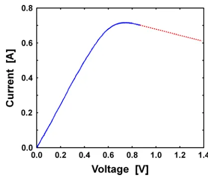
Figure2depicts a typical, room-temperatureI–V charac-teristic of a SLED from Wafer 2. No oscillations were
a)
Author to whom correspondence should be addressed: h.eisele@leeds.ac.uk
detected for bias voltages below approximately 0.85 V, repre-sented by the solid line. Oscillations were, however, observed for higher bias voltages, as indicated by the dotted line. Current values along the dotted line are only representative since they depend on the oscillation amplitude (and conse-quently RF output power). It should be noted that oscillations are still observed for bias voltages well above 1.4 V. However, RF output powers tend to decrease considerably for most oscillation frequencies, and the SLED may already exceed safe active-layer operating temperatures at this point.
RF output powers and oscillation frequencies in the fun-damental mode were measured with the WR-6 output flange of the cavity connected to a WR-6 waveguide test setup that consisted of an isolator, a directional coupler to connect to a harmonic mixer, and a thermo-couple based calorimetric power meter. All output powers were also ascertained in a second WR-6 waveguide test setup with a WR-6-to-10 wave-guide transition and a VDI Erickson PM4 power meter with a WR-10 input waveguide. A WR-5-to-6 waveguide transi-tion was connected to the WR-6 input flange of either WR-6 waveguide test setup when SLEDs in WR-5 waveguide cavi-ties were evaluated. RF output powers in a second-harmonic mode were measured with a WR-3-to-10 waveguide transi-tion between the WR-3 output waveguide shown in Fig. 1
and the aforementioned VDI Erickson PM4 power meter. Figure3summarizes the best results from Wafers 1–3 of TableIin the fundamental mode over the frequency range of 120–180 GHz. The RF output power of 4.2 mW at 145.3 GHz constitutes a 50-fold improvement over previous results.6The oscillation frequency of 175.1 GHz in a WR-5 waveguide cavity is considerably higher than the value of 155.1 GHz, the highest frequency reported previously for GaAs/AlAs SLEDs operating in the fundamental mode.10It is also approximately twice as high as the highest reported to date for GaAs Gunn devices operating in the fundamental mode (87 GHz).13
The employed full-height WR-6 and WR-5 waveguide cavities generally do not support the operation of NDR devices in a second-harmonic mode at frequencies of 110–170 GHz and 140–220 GHz, respectively. As expected from NDR devices operating in the fundamental mode, tun-ing is typically monotonic and over a wide tuntun-ing range when the position of the back short is changed.13,15–17 As can be seen from Fig. 4, the SLED from Wafer 2 with the highest oscillation frequency of 175.1 GHz can be tuned monotonically (and virtually linearly) by more than 2 GHz, i.e., from 174.67 GHz down to 172.52 GHz, when the posi-tion of the back short is changed from 0.51 mm to 0.66 mm. No mode or frequency jumps occur over the full tuning range, and an RF output power of more than 50% of the maximum is available. Such a wide tuning range is a clear indication of operation in the fundamental mode. The slight deviation from monotonic tuning around a back short posi-tion of 0.46 mm is attributed to an addiposi-tional rotaposi-tional movement (and hence some minor variation in the position) when the micrometer is turned for a translational movement of the back short plunger in the WR-5 waveguide.
[image:3.612.330.539.50.227.2]The SLEDs of Fig.3were also evaluated for their perfor-mance in the configuration of Fig.1. Figure5summarizes the best results from Wafers 1, 2, and 3 of Table Iin a second-harmonic mode over the frequency range of 240–320 GHz. TABLE I. Nominal device structures of the wafers used for millimeter-wave
superlattice electronic devices.
Wafer Number of periods Number of GaAs MLs Number of AlAs MLs Nominal doping (cm 3)
Miniband width (meV) Ref.
1 110 11 2 1.61017 180 …
2 110 11 2 1.81017 180 …
[image:3.612.52.299.79.158.2]3 110 12 2 1.51017 150 9
FIG. 1. Schematic of the WR-6 (or WR-5) waveguide oscillator cavity and WR-3 output waveguide for second-harmonic power extraction from SLEDs.
[image:3.612.322.555.590.746.2]FIG. 2. Typical, room-temperatureI–Vcharacteristics of a packaged mesa-type GaAs/AlAs superlattice electronic device from Wafer 2 on an integral heat sink.—: no oscillations;. . .: oscillations.
FIG. 3. RF output powers from SLEDs of Wafers 1 (£), 2 (䊉), and 3 (䉬) in the fundamental mode over the frequency range of 120–180 GHz.
[image:3.612.52.296.620.734.2]The highest second-harmonic frequency was 317.4 GHz with an RF output power of 77lW. This SLED also generated 4.2 mW at 145.3 GHz and 1.7 mW at 156.5 GHz, both in the fundamental mode. Similar to harmonic power extraction from InP Gunn devices,15–17the configuration in Fig.1was gener-ally the most efficient for second-harmonic generation. However, a much improved result of 0.92 mW at 249.6 GHz (Wafer 3) was achieved with a 75-lm-thick WR-6 waveguide washer between the WR-6 output flange of the cavity and the WR-3 waveguide, and 0.61 mW at 272.0 GHz (Wafer 2) was attained using a WR-6-to-3 waveguide transition instead of a washer. The use of washers and/or transitions changes the
embedding impedances seen by the SLED at the fundamental and second-harmonic frequencies from those of the configura-tion of Fig.1.
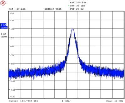
The excellent spectral purity of SLEDs at fundamental and second-harmonic frequencies was ascertained using a Rohde & Schwarz FSU-46 spectrum analyzer either with a harmonic mixer connected to the WR-6 waveguide setup or with aJ-band (170–325 GHz) harmonic mixer connected to the output WR-3 waveguide shown in Fig. 1. Figure 6
[image:4.612.329.543.50.211.2]depicts the spectrum of the SLED from Wafer 1 for an RF output power of 2.2 mW at 154.76 GHz, and Fig. 7depicts the spectrum of another SLED from Wafer 1 for an RF FIG. 4. RF output power and oscillation frequency as a function of back
[image:4.612.56.293.52.209.2]short position for a GaAs/AlAs SLED from Wafer 2 operating in a WR-5 waveguide cavity in the fundamental mode.
FIG. 5. RF output powers from SLEDs of Wafers 1 (£), 2 (䊉), and 3 (䉬) in a second-harmonic mode over the frequency range of 240–320 GHz.
[image:4.612.108.506.415.745.2]output power of 0.35 mW at 272.94 GHz. Both figures include the two traces that are produced by the (frequency) IDENTIFY function18of the spectrum analyzer. It should be noted that this method must be used with harmonic mixers to avoid erroneous results and only gives meaningful results for small frequency spans of typically less than 50 MHz depend-ing on the employed spectrum analyzer.19,20
In conclusion, both fundamental-mode and second-harmonic output powers reported in this paper are the highest to date from any SLED, and the RF output power of 4.2 mW at 145 GHz constitutes a 50-fold improvement over previous results.6 The powers in a second-harmonic mode exceed those extracted previously from higher harmonic modes by orders of magnitude, and the power of 0.92 mW in this work constitutes an improvement by 77% around 250 GHz.10
Fundamental-mode oscillation frequencies up to 175.1 GHz from Wafer 2 with a SL thickness of 0.40lm and a miniband width of 180 meV significantly exceed all previ-ously reported values. Conversely, SLEDs from Wafer 3 with a SL thickness of 0.43lm and a miniband width of 150 meV only yielded fundamental-mode oscillations up to 135 GHz. Therefore, these experimental results from Wafers 1–3 con-firm that shorter SL structures and wider miniband widths lead to higher operating frequencies. They are also a very good indication of the strong potential of SLEDs as high-performance fundamental sources for millimeter-wave and submillimeter-wave frequencies up to 1 THz. The reported RF output powers also open up the realistic possibility of
integrating SLED oscillators with SL multipliers to achieve compact THz sources.21 Further performance improvements are expected not only from fully optimized thermal manage-ment but also from SL structures designed for higher operat-ing frequencies or more efficient harmonic operation. In addition, circuit configurations that have already been demon-strated with third-harmonic power extraction from GaAs TUNNETT diodes22 and InP Gunn devices23 could be implemented.
Some of the devices were fabricated in the Lurie Nanofabrication Facility (LNF) and others at the University of Leeds. The authors thank George I. Haddad, University of Michigan, for providing access to the LNF, Kent Pruss, University of Michigan, for his precise machining of waveguides and other parts; and Pei Fen Lee for her diligent processing of some of the samples. This work was supported in part by the U.S. Army under Grant Nos. W911NF-07-1-0445 and W911NF-14-1-0614 and the UK Engineering and Physical Science Research Council.
All data supporting this study are freely available at
http://dx.doi.org/10.5518/362.
1
L. Esaki and R. Tsu,IBM J. Res. Dev.14(1), 61–65 (1970).
2H. Le Person, C. Minot, L. Boni, J. F. Palmier, and F. Mollot,Appl. Phys. Lett60(19), 2397–2399 (1992).
3
[image:5.612.107.507.57.384.2]E. Schomburg, M. Henini, J. M. Chamberlain, P. Steenson, S. Brandl, K. Hofbeck, K. F. Renk, and W. Wegscheider, Appl. Phys. Lett. 74(15), 2179–2181 (1999).
FIG. 7. Spectrum of a free-running oscillator with a SLED from Wafer 1 in a second-harmonic mode; RF power: 0.35 mW, center frequency: 272.94 GHz, ver-tical scale: 10 dB/div., horizontal scale: 1 MHz/div., resolution bandwidth: 200 kHz, and video bandwidth: 2 kHz.
4R. Scheuerer, E. Schomburg, K. F. Renk, A. Wacker, and E. Sch€oll,Appl. Phys. Lett.81(8), 1515–1517 (2002).
5
P. Siegel,IEEE Trans. Microwave Theory Tech.50(3), 910–928 (2002).
6E. Schomburg, R. Scheuerer, S. Brandl, K. F. Renk, D. G. Pavel’ev, Y.
Koschurinov, V. Ustinov, A. Zhukov, A. Kovsh, and P. S. Kop’ev,
Electron. Lett.35(17), 1491–1492 (1999).
7
M. H€außler, E. Schomburg, J.-M. Batke, F. Klappenberger, A. Weber, H. Appel, K. F. Renk, H. Hummel, B. Str€obl, D. G. Pavel’ev, and Y. Koschurinov,Electron. Lett.39(10), 784–785 (2003).
8
H. Eisele, I. Farrer, E. H. Linfield, and D. A. Ritchie,Appl. Phys. Lett. 93(18), 182105-1–182105-3 (2008).
9H. Eisele, S. P. Khanna, and E. H. Linfield, Appl. Phys. Lett. 96(7),
072101–072103 (2010).
10
H. Eisele,SPIE Proc.9585, 958508 (2015).
11
G. Bastard,Phys. Rev. B24(10), 5693–5697 (1981).
12J. Grenzer, E. Schomburg, I. Lingott, A. A. Ignatov, K. F. Renk, U.
Pietsch, U. Zeimer, B. Ja. Melzer, S. Ivanov, S. Schaposchnikov, P. S. Kop’ev, D. G. Pavel’ev, and Y. Koschurinov,Semicond. Sci. Technol. 13(7), 733–738 (1998).
13H. Eisele and G. I. Haddad, “Active microwave diodes,” in Modern Semiconductor Devices, edited by S. M. Sze (John Wiley & Sons, New York, 1997), Ch. 6, pp. 343–407.
14H. Eisele,Solid-State Electron.
32(3), 253–257 (1989).
15
H. Eisele, A. Rydberg, and G. I. Haddad,IEEE Trans. Microwave Theory Tech.48(4), 626–631 (2000).
16H. Eisele and G. I. Haddad,IEEE Trans. Microwave Theory Tech.46(6),
739–746 (1998).
17
H. Eisele and R. Kamoua,IEEE Trans. Microwave Theory Tech.52(10), 2371–2378 (2004).
18Rohde and Schwarz, https://cdn.rohde-schwarz.com/pws/dl_downloads/ dl_application/application_notes/1ef43/1ef43_0e.pdf for “Frequency Range Extension of Spectrum Analyzers with Harmonic Mixers” (accessed February 19, 2018).
19Tektronix,https://archive.org/details/tektronix_Tektronix_Spectrum_Analysis_ Using_Waveguide_Mixers for “Spectrum Analysis Utilizing Waveguide Mixers” (accessed February 19, 2018).
20
Keysight Technologies, http://literature.cdn.keysight.com/litweb/pdf/ 5988-9414EN.pdffor “External Waveguide Mixing and Millimeter Wave Measurements with Agilent PSA Spectrum Analyzers” (accessed February 19, 2018).
21
M. F. Pereira, J. P. Zubelli, D. Winge, A. Wacker, A. S. Rodrigues, V. Anfertev, and V. Vaks,Phys. Rev. B96(4), 045306 (2017).
22H. Eisele,Electron. Lett.
41(6), 329–331 (2005).
23