Theses Thesis/Dissertation Collections
2-1-2011
Electro-optic adaptive microlens
Dale EwbankFollow this and additional works at:http://scholarworks.rit.edu/theses
This Dissertation is brought to you for free and open access by the Thesis/Dissertation Collections at RIT Scholar Works. It has been accepted for
inclusion in Theses by an authorized administrator of RIT Scholar Works. For more information, please [email protected].
Recommended Citation
ELECTRO-OPTIC ADAPTIVE MICROLENS
by
DALE E. EWBANK
A DISSERTATION
Submitted in partial fulfillment of the requirements For the degree of Doctor of Philosophy
in
Microsystems Engineering at the
Rochester Institute of Technology
February 2011
Author: Dale E. Ewbank ___________________________________________________
Microsystems Engineering Program
Certified by: _____________________________________________________________
Thomas W. Smith, Ph.D.
Professor of Chemistry and Microsystems Engineering
Approved by: ____________________________________________________________
Bruce W. Smith, Ph.D. Director of Microsystems Engineering Program
Certified by: _____________________________________________________________
NOTICE OF COPYRIGHT
© 2011
Dale E. Ewbank
REPRODUCTION PERMISSION STATEMENT
Permission Granted
TITLE:
“ELECTRO-OPTIC ADAPTIVE MICROLENS”
I, Dale E. Ewbank, hereby grant permission to the Wallace Library of the Rochester Institute of
Technology to reproduce my dissertation in whole or in part. Any reproduction will not be for commercial use or profit.
Electro-Optic Adaptive Microlens
By
Dale E. Ewbank
Submitted by Dale E. Ewbank in partial fulfillment of the requirements for the degree of Doctor of Philosophy in Microsystems Engineering and accepted on behalf of the Rochester Institute of Technology by the dissertation committee.
We, the undersigned members of the Faculty of the Rochester Institute of Technology, certify that we have advised and/or supervised the candidate on the work described in this dissertation. We further certify that we have reviewed the dissertation manuscript and approve it in partial fulfillment of the requirements of the degree of Doctor of Philosophy in Microsystems Engineering.
Approved by:
Dr. Thomas W. Smith __________________________________________
(Committee Chair and Dissertation Advisor) Date
Dr. Lynn F. Fuller __________________________________________
Date
Dr. Michael Kotlarchyk __________________________________________
Date
Dr. Bruce W. Smith __________________________________________
Date
MICROSYSTEMS ENGINEERING PROGRAM ROCHESTER INSTITUTE OF TECHNOLOGY
ABSTRACT
Kate Gleason College of Engineering Rochester Institute of Technology
Degree: Doctor of Philosophy Program: Microsystems Engineering
Name of Candidate: Dale E. Ewbank
Title: Electro-Optic Adaptive Microlens
The goal of the present research was to demonstrate the viability of an electro-optic adaptive
microlens (EOAM) system in imaging applications requiring broadband illumination in the visible region.
Previous works illustrate devices that are adaptive optics but are limited in capability. Most have been
designed and optimized for a particular wavelength and many of them are polarization dependent. An
adaptive optical system that will function over a broadband of visible wavelengths will be useful in many
imaging applications.
The tasks completed for EOAM system design and build required understanding and
implementation of the imaging theory, the materials‟ properties, the control voltages, the fabrication
processes, and finally understanding and implementation of the imaging theory for testing. Single cell
transmission devices were used for initial characterization of the polymer-dispersed liquid crystal (PDLC)
process. Three iterations of the EOAM devices with PDLC were built on silicon wafers and 26 devices
were optically tested. The new chemical mechanical planarization process was implemented for the second
and third builds. For optical device testing the phase shift was extracted using a newly developed method
for blind phase extraction.
The development of a design model for the EOAM system and validating it with the images
formed by a real electro-optic adaptive microlens system has provided the knowledge base needed for
implementation of adaptive electro-optic lenses for the visible region, and a process which can be used for
further improvement of the microsystem. The model parameters can be adjusted for new electro-optic
materials that may become available that do not have the limitations of PDLC.
Abstract Approval: Committee Chair: Thomas W. Smith
Program Director: Bruce W. Smith
ACKNOWLEDGMENTS
This work is a compilation of efforts of numerous people from many different disciplines. While completing this dissertation, I am fortunate to have had the opportunity to collaborate with others and to enjoy the discovery of new knowledge. Thank you to all who have helped me with this task.
The author wishes to thank Dr. Thomas W. Smith for his time, ideas, and continuous encouragement during this dissertation process. It was an honor for me to have on my committee Dr. Lynn F. Fuller, Dr. Michael Kotlarchyk, and Dr. Bruce W. Smith.
I am grateful to the following organizations for support: KGCOE FEAD (2005), Microsystems Engineering, Electrical and Microelectronic Engineering, Imaging Science, Semiconductor and Microsystems Fabrication Laboratory.
I am indebted to my many colleagues for their help and support: Dr. Robert Pearson, Dr. Santosh Kurinec, Dr. Michael Jackson, Dr. Karl Hirschman, Dr. Sean Rommel, Dr. Surendra Gupta, Dr. Christopher Hoople, Dr. Mustafa Abushagur, Dr.
Zoran Ninkov, Dr. Jonathan Arney,Dr.Roger Easton, Robert MacIntrye, Robert Kraynik
Scott Blondell, Thomas Grimsley, David Yackoff, Bruce Tolleson, John Nash, Richard Battaglia, Sean O‟Brien, Dr. Alan Raisanen, Dan Brown, Deoram Persaud, Ivan
Puchades, Jianming Zhou, Frank Cropanese, Andrew Estroff, Neal Lafferty, Germain Fenger, Christopher Shea, and the numerous other students who helped and encouraged me.
TABLE OF CONTENTS
Abstract ... iv
List of Figures ... viii
List of Tables ... xi
I. Dissertation Statement ...1
II. Survey of Related Work ...3
III. Results and discussion ...11
A. Imaging Theory ...11
1.0 Fresnel Propagation ...11
2.0 Simulation of the EOAM system ...18
2.1 Function block diagram ...19
2.2 Assumptions for using propagation model for the EOAM ...22
B. Electro-optic Adaptive Microlens materials in single cell device ...26
C. Control voltages for the arrayed pixeldevice ...31
D. Fabrication process for the arrayed pixel device ...34
E. Device testing...45
1. Dual beam interferometer ...45
2. Single beam interferometer ...49
a. Theory ...49
b. Reflection simulation of film stack ...52
c. Imaging theory for phase extraction ...55
f. Summary of Phase extraction from devices ...67
F. Summary of EOAM Results ...72
IV. Conclusions...75
REFERENCES ...77
Appendix A:setupworkspace160_3.m, lensf500bit_3.m, arrayfillbit_160.m, fPropfocal_160.m, and address_fbit.m
Appendix B: datain_rerun_singlefile.m
Appendix C: Run Sheet for EOAM v1.5b
Appendix D: EOAM_Process Rev1_5b.PPT
Appendix E: g5_nm_PDLC.fig andg5_nm_PDLC.m
List of Figures
Figure 1: This is the conceptual design and operation of the one-dimensional LC reflection mode beam steerer. Reprinted with permission from [13] ...6
Figure 2: Fabrication of an inhomogeneous PDLC using a patterned photomask. Reprinted with permission from [14] ...7
Figure 3: Diffraction properties at = 514 nm of a prism grating made of inhomogeneous PDLC. Reprinted with permission from [14] ...7
Figure 4: Method for fabricating a PDLC Fresnel lens. Reprinted with permission from [15]. Copyright 2003, American Institute of Physics. ...8
Figure 5: Experimental setup for subjective feedback loop to improve visual acuity and determine aberrations of the human eye. Reprinted with permission from [2] ...9
Figure 6: An adaptive LC lens fabricated for experiment and 3D model of a wireless implantable LC corrector lens are shown. Reprinted with permission from [1] ...10
Figure 7: Geometry for aperture propagating to new plane ...13
Figure 8: Fresnel Wave Propagation System for Electro-optic Adaptive Microlens. ...20
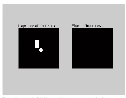
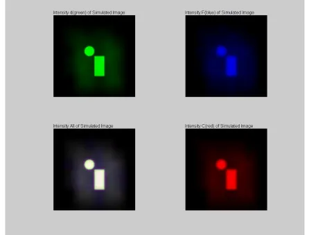
Figure 9: Input mask for EOAM system. Mask represents group of incoherent point sources with random phase and transmission of 1.0 for all wavelengths ...24
Figure 10: Sample output image for EOAM system. Simulated wavelengths are 587, 486, and 656 nm. ...25
Figure 11: Chemical structure for E48 liquid crystal. ...26
Figure 12: Chemical structure for NOA81 ...27
Figure 13: PDLC at 24% by weight in NOA81 polymerized at different intensities.
Sample transmission data includes losses due to two ITO coated glass slides. ...28
Figure 14: Image of single cell device made from E48/NOA81 utilizing patterned SU-8 resist as the spacer ...28
Figure 15: Diagram of dual beam interferometer test system used for single cell devices29
Figure 16: Phase shift versus voltage for single cell device at three wavelengths ...30
Figure 17: Comparison of phase shift with illumination of two different polarizations ...31
Figure 19: Sub array of pixels for EOAM device with 16 by 16 pixels ...34
Figure 20: Addresses for 8 by 8 array of a single quadrant with 160 micrometer pixels ..35
Figure 21: Metal 1of EOAM...36
Figure 22: Via 1 of EOAM ...37
Figure 23: Metal 2 of EOAM...38
Figure 24: Spacer layer for EOAM ...39
Figure 25: Layer stack for EOAM device...40
Figure 26: Examples of surface roughness before and after the CMP process [26] on device pixels...41
Figure 27: Hundred millimeter device wafer after all lithography steps completed ...42
Figure 28: Finished EOAM device ...48
Figure 29: Dual beam interferometer test system with device and output image on card .46 Figure 30: Device with probes in dual beam interferometer test system ...46
Figure 31: Interferogram of device from dual beam interferometer test system ...47
Figure 32: Interferogram of device from dual beam interferometer test system ...47
Figure 33: Interferogram of device from dual beam interferometer test system ...48
Figure 34: Plot showing relative phase variability from dual beam interferometer test system analysis...48
Figure 35: Single arm interferometer system diagram ... 50
Figure 36: Interferogram from EOAM device active area and surround at 0 volts ...51
Figure 37: Interferogram from EOAM device active area and surround at 200 volts ...51
Figure 38: EOAM device with non-active area masked off by black tape ...52
Figure 39: Modeled reflectance for EOAM device (entire film stack) ...54
Figure 40: Modeled reflectance for top 4 layers of EOAM device ...55
Figure 42: Phase extraction simulated with varying Ar > Ao maximum ...65
Figure 43: Phase with errors less than 2 /100 comparing input and output Ar/Ao ratio ....67
Figure 44: Layers of materials used in the reflective micro-device ...68
Figure 45: Diagram of single arm interferometer system used to collect interferograms .68
Figure 46: Interferograms of PDLC device at 3 volts (left) and 240 volts (right) ...69
Figure 47: Sample phase extraction from interferograms of electro-optic adaptive
microlens devices ...71
List of Tables
I. Dissertation Statement
The major limitations of diffractive and adaptive imaging systems presently in use
are limited wavelength bandwidth and polarization dependence of the illumination.
Diffractive optical elements (DOEs) are efficient in beam steering, phase modulation,
image formation and scanning over a limited bandwidth due to the dispersion properties
of the materials of the DOE. The adaptation of liquid crystal display (LCD) technologies
to phase arrayed imaging systems has been limited due to the polarization dependence of
LCDs. The use of adaptive electro-optic type devices for correction of human vision has
been studied [1-4] and patented [5]; however, the implementation of corrective lens
devices has not reached the consumer.
The overall goal of this research project is to demonstrate the viability of an
electro-optic adaptive microlens (EOAM) system that does not have polarization
dependence in imaging applications that require broadband illumination in the visible
region.
The specific objective is to evaluate imaging quality as a function of the pixel
array design, properties of the EOAM materials, and the applied field for each pixel in
the array. The imaging quality will be evaluated by comparison of the EOAM system
image to that of a simulated image. The cell array design parameters include pixel size,
pixel pitch, and array size, all of which ultimately define the size of the EOAM device.
The EOAM materials properties are divided into several categories: mechanical,
chemical, electrical, and optical. The mechanical and chemical properties relate mainly to
the fabrication steps involved in building the EOAM device. The optical properties are
The electrical and optical properties are the major contributors to the use and successful
application of the EOAM device in imaging. The applied field for each pixel will set the
relative phase shift for that pixel. The EOAM system is adaptive and can be used as
various type of diffractive elements by appropriate choice of the pixel array design,
properties of the EOAM materials, and the applied field for each pixel in the array.
The parameter space used in modeling and fabrication of the EOAM system lends
itself to applications in the visible region. While the electro-optic material used for this
research is not appropriate for consumer production; the knowledge developed for
modeling and fabrication is applicable to novel electro-optic materials as they become
available.
The polymer-dispersed liquid crystal (PDLC) material use in this work has
limited change in refractive index. The drive voltage and PDLC thickness combination
limit optical phase change to approximately 2 radians. This limit does not allow operation
of the EOAM at 2 levels (0, ). Thus the lensing capabilities were not evaluated for a
II. Survey of Related Work
With the slogan "you press the button, we do the rest," George Eastman put the
first simple camera into the hands of a world of consumers in 1888. In so doing, he made
a cumbersome and complicated process easy to use and accessible to nearly everyone [6].
The proliferation of optical devices over the last 120 years has grown
tremendously, largely on this same premise. There has always been a need and drive for
creating new optical instrumentation for the scientific, academic and industrial
communities; however, the needs and desires of the “consumers” are by far the largest
driving force for creation of new optical devices.
As an example, since Arthur L. Schawlow and Charles H. Townes published their
technical paper on the principles of the laser in 1958, the device has been put to work in a
vast range of applications and has assumed many forms. Today, lasers are used in a wide
range of applications in medicine, manufacturing, the construction industry, surveying,
consumer electronics, scientific instrumentation, and military systems. Literally billions
of lasers are at work today, ranging in size from tiny semiconductor devices no bigger
than a grain of salt to high-power instruments as large as an average living room [7].
Consumer optical devices are all about making cumbersome and complicated
processes easy to use and accessible to everyone. This has been done for digital cameras,
video recorders, CD and DVD players, and optical storage for computers. As the old
adage says “a picture is worth a thousand words,” and the consumer world is full of
images.
Over the past 40 years there have been two technologies that have developed and
electronic displays [8]; while optical phased array technology [9] has moved from
mechanical steering to coherent optical sensor systems.
The technological development of liquid crystal displays (LCDs) began in 1964
with the discovery of guest-host mode and dynamic scattering mode by Heilmeier of
RCA Laboratories. Heilmeier conceived the idea of manufacturing wall-sized flat-panel
color televisions. But his idea did not become a reality until 1991. Due to materials
properties and power requirements, until 1988 LCDs were limited to niche applications
of small-size displays such as digital watches and pocket calculators. The development of
twisted nematic (TN) mode, super TN mode, and liquid crystals that can operate at room
temperature broadened the number of applications. Also the development of an
amorphous silicon field-effect transistor allowed for addressing and control of the LCDs.
Using a thin film transistor array in 1988, Nagayasu [10] of Sharp Corporation
demonstrated an active-matrix full color full-motion 14 inch display. This set the new and
ever advancing standard for the notebook computer industry.
These LCDs were developed and optimized for display devices, in which the
major requirements were optical transmission and low power consumption. The optical
properties of the LC also allow for modification of polarization of the illumination and
for phase change. The polarization effects were exploited by Schadt and Helfich [11] and
the utilization of two polarizers and surface alignment of the TN mode LC is the basis for
most display manufacturing throughout the world.
In 1994 beam steering of visible light was reported using a LC television panel as
a phased array [12]. LCDs are usually configured to modulate intensity, however when
LC system was configured such that the display pixels created a discrete blazed-grating
phase ramp across the aperture. The steering efficiency and deflection angle were limited
by the large pixel size and the limited available phase modulation of 1.3 . This type of
device is also polarization dependent.
Numerous other systems have been developed and many improvements have been
incorporated. One dimensional phase modulation devices have been incorporated into
systems for two dimensional steering. These systems were designed and optimized to
solve a particular imaging problem (beam splitting or steering, scanning, focusing, and/or
correction of phase aberrations). The imaging problems must be well defined and
generally are severely constrained by their input and output environments. The system
design is usually monochromatic and thus constrained to an operating wavelength of
radiation and a very small bandwidth around that wavelength. The device size (pixel size
and number of pixels) is dictated by the required numerical aperture of the system.
A phase profile is imparted on the optical wavefront when it is transmitted or
reflected from the device. As this phase modified wavefront is propagated through the
system it converges or diverges to form an image. The refractive index changes of the LC
under an applied field allow for effective changes to the optical path length (OPL). The
change in OPL results in the change of phase for that region of the wavefront.
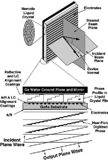
Figure 1 shows the conceptual design for a one dimensional beam steering device
developed in 1996 at a wavelength of 10.6 m with a LC phase array [13]. The device
works in reflective mode and utilizes phase wrapping of 2 . It is polarization dependent
Figure 1: This is the conceptual design and operation of the
one-dimensional LC reflection mode beam steerer. Reprinted with permission from [13].
Recent work has been done using polymer-dispersed liquid crystal (PDLC)
materials to create devices [14, 15]. The inhomogeneous nanoscale droplets of PDLC
were obtained by exposing the LC/monomer with ultraviolet (UV) radiation through a
patterned photomask as shown in Figure 2. The intensity variation during exposure of the
PDLC results in a gradient of droplet sizes in the film, and the relative refractive index
change under an applied electric field is a function of the droplet size. This gradient
refractive index nanoscale (GRIN) PDLC is highly transparent in the visible wavelengths
and has been used to create prism gratings, as well as positive, negative, and Fresnel lens.
The GRIN PDLC devices are broadband, independent of light polarization, and simple to
fabricate, however, the required driving voltage is higher than 100 Vrms and response time
Figure 2: Fabrication of an inhomogeneous PDLC using a patterned photomask. Reprinted with permission from [14].
The optical results for a GRIN PDLC device are shown in Figure 3. The prism
grating is formed by the gradient of refractive index due to the patterned polymerization
resulting in control of the LC droplet sizes. The grating is “on” with no field applied and
the applied field of 100 volts causes the LC droplets to align and cancel the index
gradient.
Figure 3: Diffraction properties at = 514 nm of a prism grating made of inhomogeneous PDLC. Reprinted with permission from [14].
A Fresnel lens was also fabricated using the GRIN PDLC as shown in Figure 4.
The lens is patterned to control droplet size and thus phase in 80 zones. As with the
grating above, the entire device is controlled with a single applied field. These devices
Figure 4: Method for fabricating a PDLC Fresnel lens. Reprinted with permission from [15]. Copyright 2003, American Institute of Physics.
Systems for phase modulation have also been demonstrated by using LC on
silicon technology [16] and spatial light modulators (SLM) built with optically
addressable LC cells [17]. These systems have shown excellent results in wavefront
phase modulation and have two-dimensional array control; however, they are polarization
dependent. And because the LC system is based on light scatter they suffer from limited
efficiency of light transfer.
One of the applications for wavefront phase modulation is correction for human
vision. An adaptive optics phoropter system has been demonstrated utilizing optically
addressable LC SLM [18]. The system is used to measure the wavefront errors that occur
due to the structure of the human eye. The adaptive optics allow for correction of the
lower-order aberrations of the eye (defocus and astigmatism) as can be done using a
high-order aberrations such as spherical aberration and coma, leading to near
diffraction-limited image quality at the retina.
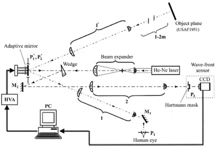
Figure 5 shows the test bench design for a correction system with human
feedback for control of a deformable mirror for wavefront control [2]. The system is
designed to correct wavefront errors that limit human vision and to establish the
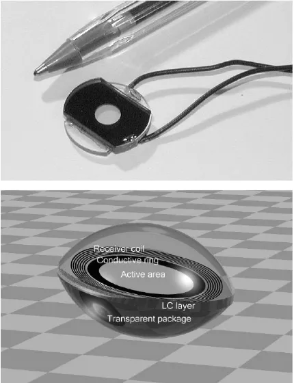
correction values needed for proper wavefront control. Vdovin has also done work in the
field of applying these corrections by building adaptive lens [1]. As seen in Figure 6, a 5
mm aperture LC adaptive lens was fabricated. The lens is addressed by a single applied
field and only focal length can be controlled. This LC system is also polarization
[image:21.612.109.539.346.640.2]dependent.
Figure 6: An adaptive LC lens fabricated for experiment and 3D model of a wireless implantable LC corrector lens are shown. Reprinted with permission from [1].
The previous works illustrate devices that are adaptive optics but are limited in
capability. Most have been designed and optimized for a particular wavelength and many
of them are polarization dependent. An adaptive optical system that will function over a
broadband of visible wavelengths and be polarization independent will be useful in many
III. Results and discussion
The five major topics of the solution are understanding and implementation of the
imaging theory for design, the materials‟ properties, the control voltages for the device,
the fabrication process, and finally understanding and implementation of the imaging
theory for testing. Each of these topics will be discussed in this section.
A. Imaging Theory
An essential element of this research project is the design, modeling, and
fabrication of an EOAM system for use in the visible wavelengths of light. An EOAM
that will function over a broad range of applications can reduce the cost of production
and ultimately reduce the cost of ownership for the system.
1.0 Fresnel Propagation
The optical modeling for the EOAM system is based on Fresnel propagation
[19-22]. The device design was stimulated and the imaging system was modeled and
compared to the desired output (image). In an iterative process the design can be
changed, simulated, remodeled and compared to allow for optimization of the EOAM.
The design changes can be driven by various optimization schemes.
Viewing wave propagation phenomena as a system allows for valid
approximations over a wide class of input field distributions and optical elements. The
concept of the intensity of a wave field and the Huygens-Fresnel principle are well suited
for approximation in image formation. The first wave theory for light expressed by
Christian Huygens in 1678 was that if each point on a wavefront is considered as a point
source radiating spherical wavefronts, then a later wavefront can be found by
The response of a detector is a function of the distribution of the intensity in the
image. Thus it is important to relate the intensity to the complex field which makes up the
image.
In 3-dimensional space the second order partial differential wave equation is
(3.1.1)
and the generalized harmonic wave is
(3.1.2)
where represents a position vector of a point in space. At any fixed time,
the surfaces for which equals a constant are called wavefronts. When , the
amplitude of the wave, is a constant over the wavefront, the wave is homogeneous.
The above generalized harmonic wave can be expressed in complex form as
(3.1.3)
where
(3.1.4)
with equal to an initial arbitrary phase.
This is useful when substituting into (3.1.1) resulting in
which is the Helmholtz Equation. If interested in the spatial properties, but not the
temporal, solutions to the Helmholtz Equation are sufficient to represent the wave.
The Huygens-Fresnel principle can be stated in rectangular coordinates as
(3.1.6)
where the angle between the outward normal and the vector pointing from to as shown in Figure 7. represents the field at the plane of having
Figure 7: Geometry for aperture propagating to new plane.
propagated from the plane at . The value of and (3.1.6) can be rewritten as
(3.1.7)
where the vector distance is given by
(3.1.8)
z
y
x
0y
0x
z
0=0
z = z
1Huygens-Fresnel principle has only two approximations: one is the approximation
inherent in scalar theory and the second is the assumption that as the observation
plane is many wavelengths form the aperture.
The distance can be approximated by making use of the binomial expansion
for the square root. For the number of terms needed in the expansion
, (3.1.9)
for accuracy depends on the magnitude of . Applying the expansion to (1.8) yields
(3.1.10)
by retaining the first two terms. When substituting (3.1.10) into (3.1.7) the error of the
value for squared in the denominator is small provided ,
which is the case in the paraxial region. However, the in the exponent is multiplied by
a large , and phase changes of small fractions of a radian change the value of the
exponential significantly. Both terms in the binomial approximation must be kept in the
exponent. The expression for the field by substituting (3.1.10) into (3.1.7) becomes
By rearranging and incorporating the finite limits of the aperture in the definition of
the resulting equation is
. (3.1.11)
The field at any plane z1described by (3.1.11) can be seen as a convolution of
the form
(3.1.12)
with the convolution kernel as
. (3.1.13)
The expression for represents a diverging spherical wave and quadratic phase
approximation to the wave for position values of . The convolution with (3.1.13) is the
propagation of the field from the aperture at plane to the field at
for the plane at .
Maxwell‟s Equations lead to the properties of light [19-22]: its wave nature, that it
is a transverse wave, and the relationship between the electric and magnetic fields.
Assume light propagating in a medium that has the following properties:
Uniform: , permittivity (dielectric constant,) and , permeability, have constant value at all points
Isotropic: and do not depend on direction of propagation
Nonconducting: , conductivity, and thus , current density
Free of “free charge”: , charge density
Then Maxwell‟s Equations are:
(3.1.14)
(3.1.15)
(3.1.16)
(3.1.17)
Evaluating Maxwell‟s Equation in a medium leads to the following two equations
(3.1.18)
, (3.1.19)
which are coupled transverse waves. The electric and magnetic field are also solutions to
the Helmholtz and 3-dimension second order partial differential wave equation for
vacuum when
. (3.1.20)
For materials where , velocity, is less than , velocity in vacuum, the material
is characterized by its index of refraction,
. (3.1.21)
The intensity of the field is related to the flow of energy for the coupled electric
. (3.1.22)
The Poynting vector cannot be detected at the very high frequencies associated with light,
so what is detected is the temporal average of taken as an average over time, ,
determined by the detector time response. The time average of is the flux density in
units of [W/m2] and is called intensity of the light wave,
. (3.1.23)
For an electric field represented by and using the
expression for intensity can be reduced to
(3.1.24)
where . Then for independent of time and ,
. (3.1.25)
Knowing that for large the integral , results in
. (3.1.26)
The intensity of the field is proportional to the electric field amplitude squared.
In actual practice the electric field at the object plane must be broken down into
constituent parts for modeling. The above Fresnel propagation is based on
definition of for (3.1.11), also assumes that the aperture can be adequately
described.
For broadband illumination in the visible region the propagation can be simulated
at multiple wavelengths. Then a summation of the multiple wavelength aerial images
approximates the actual image well. The difficulty in this scenario is the estimation of
temporal coherence.
To adequately describe the illumination field at aperture, , for the case when the
field is spatially coherent is relatively easy. An arbitrary phase can be assigned as in
(3.1.4). However, for the spatially incoherent field this is not possible. In the spatially
incoherent field case it is useful to evaluate the EOAM system as if the illumination field
is a point source, and to use the aerial image of that point source as the system response.
The system response from the point source is valid for spatial coherence; however, the
effects of temporal coherence may introduce errors. The image from the aperture, , can
then be approximated by proper sizing (magnification) and convolution with the system
response as Fresnel propagation is linear and shift invariant [20].
2.0 Simulation of the EOAM system
The purpose of the system is to create an aerial image for a finite amount of time
that can be captured by another system for viewing, propagation or as a latent image. A
wavefront (electro-magnetic field) and a mask are the inputs to the system. The output is
an aerial image that has characteristics unique to the system inputs. The desired image is
a result of the transfer of the wavefront and mask as well as the interactions of the various
image or it may be designed to contain information that changes the wavefront unique to
the system.
The input wavefront is allowed to enter the system for a finite time by the
exposure control unit. The mask in the filter interface then modulates this wavefront. The
resulting modified wavefront is then propagated a distance z1. The propagation of the
wavefront results in a redistribution of the energy in the wavefront. The EOAM function
then collects the energy and modifies the wavefront. The wavefront leaving the EOAM is
then propagated a distance z2. The wavefront output is an electro-magnetic field that has
an energy distribution that can be viewed, propagated, or captured.
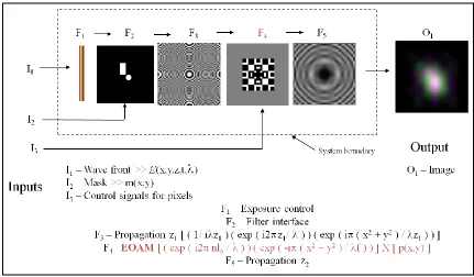
2.1 Function block diagram
The function block diagram in Figure 8 illustrates the system relationships used in
the simulation and for the physical EOAM device. Each of the components (inputs,
output, and functions) is described in this section.
I1 – Wavefront
The wavefront is an electro-magnetic wave that is described in four-dimensional space.
The wavefront is known by its electric component, which is a complex vector field,
, as a function of three-dimensional space and time. The wave must follow
Figure 8: Fresnel Wave Propagation System for Electro-optic Adaptive Microlens
I2 – Mask >>
The mask is a physical object that can modify the electro-magnetic wave. The mask is
described by which is a two-dimensional array of complex numbers.
I3 – Control signals for pixels
The EOAM device is controlled by addressing the array of pixels with various applied
voltages. The applied voltage determines the relative phase shift introduced into the
wavefront by each of the pixels.
F1 – Exposure control
The exposure control function allows for the input wavefront into the system and to
transfer energy for a finite amount of time. The function is modeled by a rectangle
function, . The output is the result of multiplied by .
The wavefront and mask are input into the filter interface. The interface controls the
alignment of the two components and can be modeled by a multiplication of
by . The output of the filter interface is a modulated wavefront.
F3 – Propagation
The propagation function models the transfer of the wavefront through a medium. The
medium is described by its optical properties, namely optical path distance , and the
propagation is modeled by a convolution with the modulated wavefront.
(3.1.27)
(3.1.28)
F4 – EOAM
The EOAM element changes the wavefront by modifying the relative phase at each pixel.
The model for the EOAM function is the multiplication of the wavefront with the pupil
and the EOAM element. The pupil is a two-dimensional complex array that limits the
energy transferred from the incoming wavefront to the output wavefront. The EOAM
element changes the characteristics of the wavefront.
(3.1.29)
F5 – Propagation
The propagation function models the transfer of the wavefront through a medium. The
(3.1.30)
(3.1.31)
O1 – Image
The image is an electro-magnetic field that is known by its electric component, which is a
complex vector field, . Here the intensity is proportional to electric field
squared,
. (3.1.32)
2.2 Assumptions for using this propagation model for the EOAM
The model was implemented in Matlab® code with the following assumptions:
a) Fresnel propagation
b) Polarization independence
c) Paraxial region for object and image
d) Wavelength dependence
e) Spatially incoherent illumination.
The first three assumptions are based on the theory in section 1.0, Fresnel Propagation.
This code is shown in Appendix A: setupworkspace160_3.m, lensf500bit_3.m,
arrayfillbit_160.m, fPropfocal_160.m, and address_fbit.m.
The wavelength dependence of the equations is handled by simulation at three
completely through the system and the intensity is found at the image plane. The final
image is a summation of the three wavelength intensities.
For spatially incoherent illumination each point of the mask can be treated as an
independent point source with random phase. In the paraxial region of the system the
image can be approximated by the convolution of the point spread function of the system
with the appropriately scaled object. The scaling is based on geometric optics for a
simple thin lens. Figure 9 and Figure 10 show sample input and output for a focal length
500 micron lens with 256 by 256 micron square pupil having pixel size of 4 microns and
dispersion index similar to quartz. The phase has been quantized to 4 levels between zero
and 2 , with the regions between pixels approximated by averaging the phase of the
adjacent pixels. The object and image distances are based on geometric paraxial Gaussian
B. Electro-optic Adaptive Microlens materials in single cell device
The EOAM materials properties are determined by mechanical, chemical,
electrical, and optical factors. The mechanical and chemical characteristics relate mainly
to the fabrication steps involved in building the EOAM device. Because the device was
patterned using lithography, the optical properties are also determined during fabrication.
The electrical and optical properties are the major contributors to the performance and
ultimate utility of the EOAM device in imaging.
The electro-optic material used in the device is a polymer-dispersed liquid crystal
(PDLC) described by Ren et al[15]. A mixture of 26% by weight E48 LC and 74% UV
curable prepolymer NOA81 was sandwiched between ITO coated glass slides and
patterned to create a GRIN PDLC Fresnel lens. Figures 11 and 12 illustrate the structures
of the molecular entities of E48 and in NOA81. The mixture was patterned by exposure
with UV radiation that induced the monomers in NOA81 to polymerize. The rate of
polymerization determines the droplet size of the micro domains of LC material that
phase separate as the NOA81 polymerizes. It has been confirmed in the literature [23, 24]
that the mean size of the droplets is dependent on the weight fraction of LC and the rate
of polymerization.
CN
4-cyano-4'-pentyl-1,1-biphenyl
S H
O
O
SH
O
SH O
O
O
O
O
OH Composition of a thioester UV curable photoresist
+ + Photoinitiator
Figure 12: Chemical structure for NOA81.
Several composite films (Samples 001-005) with 10 micrometer polystyrene
spheres used as spacers on the substrate were cured and used for preliminary studies on
single cell devices. The samples were exposed with a mercury arc source filtered at 365
nm. Because the droplet size of the micro domains of LC were slightly larger than the
wavelength of illumination, Sample 001, exposed at intensity of ~2.25 mW/cm2,
appeared somewhat milky in color under white light illumination and the LC droplets
scatter the light. In Sample 005, exposed at intensity of >50 mW/cm2, the droplet size
was equal to or smaller than the wavelength of visible light and appeared clear. Figure 13
shows transmission data collected on the two samples. Sample 005 had higher
transmission but exhibits some loss of transmission at shorter wavelengths. This indicated
that the droplet size was approximately on the order of the blue wavelengths.
The next generation of single cell devices (shown in Figure 14) were fabricated
utilizing patterned SU-8 photoresist as a spacer on the ITO glass slides and the
Figure 13: PDLC at 24% by weight in NOA81 polymerized at different intensities. Sample transmission data includes losses due to two ITO coated glass slides.
Figure 14: Image of single cell device made from E48/NOA81 utilizing patterned SU-8 resist as the spacer.
The samples were also evaluated using a Michelson interferometer to determine
measurement arm of the Michelson interferometer and a voltage was applied to the ITO
layer of one slide, while the other ITO slide was grounded. The light path made a double
pass through the sample with this configuration as shown in Figure 15.
Figure 15: Diagram of dual beam interferometer test system used for single cell devices.
The interferograms from the dual beam interferometer were captured on a digital
camera back and analyzed using code written in MATLAB®. This code (Appendix B,
datain_rerun_singlefile.m) allowed selection of an area of multiple interferograms for
analysis of minimums and calculation of the relative shifts of the minimums. The
interferograms were captured with different applied voltages and a sample of the output
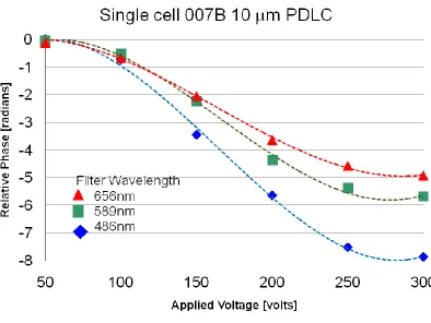
phases fit to 3rd order splines is shown in Figure 16. A system to measure phase for
reflective electro-optical micro-devices at visible wavelengths was presented at Optical
Figure 16: Phase shift versus voltage for single cell device at three wavelengths.
The single cell device was also evaluated at the red wavelength for sensitivity to
polarization of the illumination. The PDLC as fabricated is reported to be polarization
independent [15]. Interferograms were captured for the device with a linear polarizer
inserted in the beam path ahead of the beam splitter. The resulting relative phase versus
applied voltage is shown in Figure 17. A 100%(1- ) confidence interval, with = 0.05,
was constructed on the regression of Relative Phase on Applied Voltage for P270. This
confidence interval was used to compare the 3rd order fit for P0 to the 3rd order fit for the
P270 regression. It was found that the estimated fit for P0 fell entirely within the 95%
confidence interval for P270, so no significant difference between the two processes can
be discerned at the = 0.05 level. Note that this confidence interval is a realization of all
regression (not the individual observations) will fall within the estimated upper and lower
bounds of the interval.
Figure 17. Comparison of phase shift with illumination of two different polarizations.
C. Control voltages for the arrayed pixel device
The applied field for each pixel of the EOAM controlled the relative phase for
that pixel. The simulation program (Appendix A, address_fbit.m) for addressing of pixels
in the device array at various phase levels was written to incorporate the relative phase
shift as a function of the material thickness, the applied field and the wavelength of
illumination. The number of required phase levels for operation of the system was
quantized and also incorporated in the simulation.
To simplify the addressing of the device the work utilized only two phase levels.
The imaging performance of the EOAM system can be enhanced by allowing more phase
-6 -5 -4 -3 -2 -1 0 1 2
0 50 100 150 200 250 300
R
elat
iv
e
p
h
ase
[r
adia
n
s]
Applied voltage DC [V]
EOAM 007B Phase with polarized
illumination
p0
p270
95% CI on p270
Poly. (p0)
levels. A voltage control device that allowed quantization of the applied field at 22 levels
was built on a breadboard for use in testing the EOAM devices.
The power distributor design was based on the need to use one power supply with
multiple outputs. The EOAM devices use applied voltage over a range of 0 to 300 volts
AC or DC but do not conduct current. Accordingly, the distributor was designed for
safety to limit current to less than 1 mA. If the EOAM device has current flow, it has
failed and is no longer useable. Slow blow 10 mA fuses were assembled in-line on the
power source leads, and ~300 k ohms resistors were added to the EOAM leads. The
power supply varied from 0 to ~240 volts, and the distributor board was designed to have
four levels plus ground. Figure 18 shows a diagram of the voltage distribution board. The
voltage at each node for the EOAM is as follows:
(3.2.1)
where R1 is the resistance before the node and R2 is the resistance after the node with the
Figure 18: Diagram of voltage distribution board for EAOM device.
DC voltage was used in testing the single cell devices and the first fabrication run
of the 16 by 16 pixel devices. As the single cell and pixel devices had a long memory
(> 30 seconds to return to off state) with DC applied voltage, the subsequent pixel
D. Fabrication process for the arrayed pixel device
The fabrication processes for the EOAM made use of both newly developed and
existing processes within the Semiconductor and Microsystems Fabrication Laboratory at
RIT. Detailed instructions for the fabrication processes are given in Appendix C, Run
Sheet for EOAM v1.5b, and illustrations of the fabrication processing steps are shown in
Appendix D, EOAM_Process Rev1_5b.PPT.
Figure 19: Sub array of pixels for EOAM device with 16 by 16 pixels.
Figure 19 shows a sub array of 8 pixels (a through h) that are addressed
individually. These are built up to create the four quadrants of the device. The routing
layout for the device was optimized for the sub array. For a lens that is circularly
symmetric to the optical axis, this arrangement of cells allows for multiplexing of the
cells that are of equal radial distance from the optical axis (usually the center of the device). The code „address_fbit.m‟ calculates the quantization levels for the lens phase
addressing a single quadrant for a 250 mm focal length microlens for phase quantized at
2 and 4 levels.
Figure 20: Addresses for 8 by 8 array of a single quadrant with 160 micrometer pixels.
The design for wiring to bond pads utilized ICgraph by Mentor Graphics
Corporation. Four sets of bonding pads are on the device, however access is only needed
to one set. The others are redundant and also allow for redundant multiple contacts
between the metal layers.
Figure 24 Spacer layer for EOAM.
The fabrication process had 4 levels that required microlithographic patterning.
Figure 25 is a diagram of a complete layer stack for one pixel. Metal 1 is the wiring for
addressing the pixels. Metal 2 is the conductor that defines the lower electrode for each
Figure 25 Layer stack for EOAM device.
After fabrication of the first devices it was found that the metal 2 layer had a
surface roughness that was too large and the variation in surface height of the pixel due to
the contacts resulted in large optical path variations. This layer is the reflective mirror in
the device and as such, should have specular rather than diffuse reflections. A new
process was developed and implemented to polish the metal 2 surface. The thickness of
the deposited aluminum was increased to 1.5 micrometers from 1.0 micrometers to
ensure step coverage over the metal 1 and contact edges, and still allow for removal of
metal 2 material. The chemical mechanical planarization (CMP) of the metal 2 was done
on the Strausbaugh. This CMP process was optimized and was unique in the fact that the
aluminum layer was patterned before CMP. If the metal was planarized first, then
Figure 26: Examples of surface roughness before and after the CMP process [26] on device pixels.
The devices were probed prior to CMP to verify the proper conductivity between
the pads and the appropriate pixels for the device design. This allowed for sorting of good
devices before CMP and also prevented scratching of the planarized surface.
After CMP the spacer layer was patterned in SU-8 photoresist. The SU-8 is a
negative photoresist and was cross linked with exposure at i-line and post development
baking. A sample wafer completed to this step is shown in Figure 27. The SU-8 pattern
Figure 27: Hundred millimeter device wafer after all lithography steps completed.
The E48/NOA81 mixture was deposited as a liquid and covered with the ITO
glass slide. Photopolymerization of the PDLC bonds the ITO glass slide in place. A
specialty UV exposure tool was assembled for use in photopolymerization of the
E48/NOA81 mixture. This tool allowed for controlled intensity and thus control of the
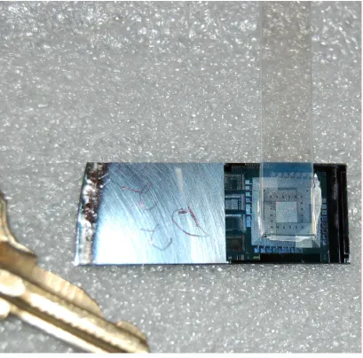
rate process for droplet formation of the LC domains. Figure 28 show a finished EOAM
Figure 28: Finished EOAM device.
Detailed instructions for the fabrication processes are given in Appendix C, Run Sheet for
EOAM v1.5b and illustrations of the fabrication processing steps are shown in Appendix
D, EOAM_Process Rev1_5b.PPT.
Arrayed pixel device builds
The fabrication of the arrayed pixel EOAM devices was carried out with three
and were rebuilt. The first iteration of EOAM devices could only be tested with all pixels
addressed to same voltage. The surface roughness for the Metal 2 layer was also
identified with the initial run.
The second iteration implemented the new masks, the CMP process, and adjusted
film thicknesses of the layers to allow CMP. The third iteration repeated the processes
used and greater care was taken to reduce contamination defects and improve yield to
E. Device Testing
1. Dual Beam Interferometer
While each new build was ongoing, devices from the previous run were used for
evaluation of phase versus applied voltage. The phase extraction method of using
multiple interferograms with various applied voltage for analysis of minimums and their
relative shifts as used for the single cell device was implemented for the pixel arrays
addressed with same voltage. The results from this method proved to be unreliable.
Changes in the optical path lengths of the dual beam interferometer system due to
vibration and ambient temperature fluctuations caused the relative phase shifts to be
unrepeatable.
Figures 29 and 30 show a device in the dual beam interferometer test system.
Figures 31 through Figure 33 are interferograms captured for a pixel device with all
pixels address by same voltage. Figure 34 shows a plot of data from analysis of the
interferograms from the dual beam interferometer. The line connects the data point in the
order that the interferograms were collected (total time of about 10 minutes). As can be
Figure 29: Dual beam interferometer test system with device and output image on card.
[image:58.612.109.342.401.682.2]Figure 33: Interferogram of device from dual beam interferometer test system.
Figure 34: Plot showing relative phase variability from dual beam interferometer test
[image:60.612.110.543.429.630.2]2. Single Beam Interferometer
a. Theory
A new method for extraction of the phase was needed. During the set up of the
dual beam interferometer system it was noted that interference patterns could be
generated by utilizing only the EOAM device in a single arm of the interferometer. The “surface” reflection of the device was known to exist; but had been considered as a
nuisance reflection and needed to be minimized as it contributed to the „noise‟
component during device measurement and usage. With the dual beam system the
reference beam wavefront and the device beam wavefront were to recombine and
generate the appropriate interferogram; the “surface” reflection wavefront was 5 to 10
times less intense and to be neglected.
The reference beam mirror was taken out of the dual beam interferometer system
to create the single arm interferometer system. The EOAM device acts as a Pohl
fringe-producing system [22] that can generate interferograms. The use of a single arm
interferometer system for reflective micro-device phase measurement was presented at
Optical Fabrication and Test Conference in 2010 [27]. Figure 35 shows a diagram of the
Figure 35: Single arm interferometer system diagram.
Figures 36 and 37 show interferograms from the device tested in the single arm
interferometer system. The interferograms include the active device area and the
surrounding non-active electrical pad area (right side of image); the non-active area
interferogram does not change with applied voltage. The non-active areas were masked
Figure 38: EOAM device with non-active area masked off by black tape.
b. Reflection simulation of film stack
The interferograms from the EOAM devices at varying voltage clearly show
changes to the interference patterns. The interferograms are the result of constructive and
destructive interference between the wavefront of the active device optical path and the
wavefront of the non-changing optical path (reference wavefront) in the single arm
interferometer system. Simulation code was written in Matlab® to explore the
Appendix E, g5_nm_PDLC.fig andg5_nm_PDLC.m. The optical properties of the film
stack for the EOAM device are input and the algorithm models the reflectance [19] at the
various interfaces based on the layers of the film stack. Figure 39 shows the estimate for
reflectance into air of the EOAM device versus thickness of the ITO layer for 541 nm
illumination at 2 degrees angle of incidence as 0.84 to 0.91. This reflectance estimate
includes the active device optical path and the wavefront from the non-changing optical
path. Figure 40 gives the reflectance, 0 to 0.06, for the wavefront from the non-changing
Figure 40: Modeled reflectance for top 4 layers of EOAM device.
c. Imaging theory for phase extraction
Extraction of the blind phase from the interferograms was necessary to
characterize the EOAM as a function of the applied voltage. An iterative algorithm
(Appendix F, xu_2007_ph_ext_05182010_data_p.m) has been implemented for blind
EOAM was designed to operate in the visible wavelengths and due to its reflective nature
it was possible to collect interferograms of the reference wavefront and the object
wavefront using a common optical path. It is not possible to measure the reference and
the object wavefronts independently for the reflective device; and therefore the algorithm
has been developed for this case. To validate the code and better understand its region of
usefulness a series of simulations were completed to verify the algorithm based on
assumptions.
Evaluation of optical surfaces is commonly accomplished via phase-shifting
interferometry (PSI). PSI techniques have been used for more than forty years [28, 29].
All PSI techniques are based on multiple collections of the interference of a reference
wavefront and an object wavefront at some point in space. An interferogram is a mapping
of one of these collections of interference.
In general each interferogram, collected as an image, is a record of the constructive
and destructive interference of the reference and object wavefronts at a plane for some
finite interval of time. The image irradiance collected at each point (x,y) of the detector is
given by:
(3.4.1)
where (x,y) is the relative phase of each image point and is the relative phase
difference between the reference and object wavefronts. Ao(x,y) is the electric field of the
object wavefront and Ar is the electric field of the reference wavefront. It is assumed
that the reference wavefront is non-varying across the image.
Many of the modern methods of PSI require collection of multiple (n ≥ 3)
wavefronts. The requirement for multiple interferograms is due to the mathematical
methods used for extraction of information from the interferograms. Equation (3.4.1) has
four unknowns and thus requires three or more images to develop a solution.
There are techniques that can derive the wavefront or extract the phase difference
utilizing only two interferogram images [37, 38]; however these techniques require that
the reference wavefront and the object wavefront be measurable independently of one
another.
A method utilizing an iterative algorithm for blind phase extraction [39] allows for
extraction of the phase without measurement of the reference wavefront. This method
was used as the starting point for development of a technique to extract phase for an
electro-optic micro device that functions in the visible and is also reflective.
The electro-optic micro device [27] was fabricated on a silicon substrate and allows
for addressing of pixels. The device has an active layer of polymer dispersed liquid
crystals (PDLC) that change alignment under an applied electric field. The alignment of
the PDLC causes a change in the refractive index and thus alters the effective optical path
length. The device is reflective and the incoming radiation makes a double pass through
the PDLC before exiting.
To characterize the change in optical path length with applied electric field the device
was put into a Twyman-Green (dual beam) interferometer that was assembled on an
electrical probe station [25]. Upon measurement and calculation of the phase change of
the micro device, with replication of the results it was found that the arms of the
interferometer were not stable. The extracted phase in data collected over a period of 20
In the optical setup and alignment process it was also noted that reflections from other
surfaces of the device allow for collection of interferometric fringes. These “nuisance”
fringes are a result of the upper layers of the electro-optic micro device and are noise to the device output. However, this ”nuisance” wavefront can be used as a reference
wavefront in a single beam interferometer system [27]. This reference wavefront cannot
be measured independently of the object wavefront exiting the device.
A modified algorithm has been developed and tested. This new technique allows for
relative phase extraction of the active layer of the micro device while utilizing the “nuisance” wavefront as the non-changing reference. This new technique is based on the
blind phase shift extraction [39] technique previously published; however it requires a
different set of assumptions., which are discussed in detail in the following section. The
modified algorithm was tested via simulated interferograms and a comparison of
extracted phase shifts to known inputs. Data is presented for extracted phase shifts from
the reflective electro-optic micro device.
d. Assumptions and algorithm
The previously published iterative algorithm for blind phase extraction [39] combines
the least square regression method and formulae that allow extraction of the unknown
phase shift utilizing only the intensities of the two interferograms. While the algorithm
requires far less measured or controlled input than other methods [28-38], it has a few
stated assumptions and restrictions.
Equation (3.4.1) is the basis for the two required interferograms and are given as
(3.4.2)
(3.4.3)
I1(x,y) is given for = 0, where as I2(x,y) includes a change in phase equal to . The
algorithm [39] previously published requires that the following assumptions hold true:
I. Ao(x,y) and (x,y)are the real amplitude and phase distributions of the
object wave and the region of interest is large enough that the distribution of is random.
II. Ar is the constant amplitude of a plane reference wave.
III. The arbitrary phase shift of the reference wave between two images is and 0 < <
IV. Inputs of Ar > Ao maximum, as is the case in practice to guarantee correct
recording.
As stated, the algorithm previously published works well over a wide range of phase
shift from 0.4 to 2.5 radians [39].
In this work the use of the algorithm has been extended to the case for the reflective
electro-optical adaptive micro-device. As such, the algorithm requires the two
interferograms given in equation (3.4.2) and (3.4.3) as well as the following assumptions:
i. Ao(x,y) and (x,y) are the real amplitude and phase distributions of the
object wave and the region of interest is large enough that the distribution of is random.
ii. Ar is the constant amplitude of an unchanging reference wave.
iii. The arbitrary phase shift of the object wave between two images is and 0 < <
iv. Calculated Ar /Ao ratio of greater than one.
v. Calculated values in the iterations of the least squares regression must remain real valued.
This modified algorithm works well over a wider range of phase shift depending on
Assumption I and i are the same as both algorithms are designed to extract the phase
change between the reference wavefront and an object wavefront based on equations
(3.4.2) and (3.4.3).
Assumption II, III, and IV are required because the initial algorithm is designed to
extract the object wavefront, which can be back propagated to calculate the amplitude
and phase distribution of the object. For this work the amplitude of the object wave and
reference wave are assumed to be non-changing as the object is shifted in phase by
between the two interferograms. Therefore assumptions II and III are changed to
assumptions ii and iii.
Assumption iv is required due to the reflective nature of the electro-optic micro
device. However, as stated in [29, 38] and inferred by many using PSI, wavefront
reconstruction by two-step interferometry requires Ar(x,y) to be chosen as a constant
greater than the maximum of Ao(x,y). This is due to the image recording method on silver
halide film. Due to the non-linearity of the foot of the image transfer curve the beam
ratio,
(3.4.4)
is stated in [40] as requiring a minimum R > 1. This requirement has been carried over
for the use of digital image detectors, even though most digital detectors are linear down
to much lower irradiances. For dual or multiple beam interferometers the wavefronts can
be attenuated to ensure the beam ratio remains greater than one. Attenuation of the
wavefronts independently is not possible with a single beam system as used with a
Assumption v is applied as a result of using the algorithm on simulated and
experimental data. Further explanations and examples follow.
Following the algorithm [39], using equations (3.4.2) and (3.4.3), the sum and the
difference of the two interferograms are
(3.4.5)
and
(3.4.6)
Using assumption i and sin2[ (x,y) - ] + cos2[ (x,y) - ] = 1 with equations
(3.4.5) and (3.4.6), the quadratic equation
(3.4.7)
is obtained, where Io= Ao2, Ir= Ar2, p = I1 + I2 + 2 Ircos( ), q = [(I1 + I2 - 2 Ir)2 + (I2 -
I1)2/tan2( )]/4, and the coordinates (x,y) are omitted from Ao, Io, I1, and I2. Solving for
the real roots by assuring and are positive as in [39], the
irradiance and electric field are found for the object wavefront,
(3.4.8)
Here assumption iv is used; validation will be shown in the simulations.
Rearrangement of equation (3.4.2) gives
(3.4.9)
and
(3.4.10)
The object wavefront O(x,y) = Ao(x,y) exp(i (x,y) can be calculated with I1, I2, Ar and
using equations (3.4.8)-(3.4.10).
Least squares regression can be used to find Ar and by rearrangement of equation
(3.4.6) as
(3.4.11)
where
(3.4.12)
and the summations for equation (3.4.13) are taken for the N x N pixels of the
interferograms. The matrix,
(3.4.13)
can be solved for values of Ir, c1, and c2 allowing calculation of the reference electric field
Ar and the phase shift as
(3.4.14)
Thus using I2, Ao and the blind phase shift is extracted.
Because only the interferograms I1 and I2 are known, the initial value for is chosen
from 0.1 to 0.4 times and the initial value for Ar is the square root of the average pixel
irradiance of I1(x,y). With these initial values, Ao and are calculated using equations
(3.4.8)-(3.4.10). The least squares regression is then calculated and new values for the