The role of chemical structure on the magnetic and electronic properties of
Co2FeAl0.5Si0.5/Si(111) interface
Balati Kuerbanjiang, Zlatko Nedelkoski, Demie Kepaptsoglou, Arsham Ghasemi, Stephanie E. Glover, Shinya Yamada, Thomas Saerbeck, Quentin M. Ramasse, Philip J. Hasnip, Thomas P. A. Hase, Gavin R. Bell, Kohei Hamaya, Atsufumi Hirohata, and Vlado K. Lazarov
Citation: Appl. Phys. Lett. 108, 172412 (2016); doi: 10.1063/1.4948466 View online: https://doi.org/10.1063/1.4948466
View Table of Contents: http://aip.scitation.org/toc/apl/108/17
Published by the American Institute of Physics
Articles you may be interested in
The antiphase boundary in half-metallic Heusler alloy Co2Fe(Al,Si): atomic structure, spin polarization reversal, and domain wall effects
Applied Physics Letters 109, 222405 (2016); 10.1063/1.4971281
Improvement of magnetic and structural stabilities in high-quality Co2FeSi1-xAlx/Si heterointerfaces
Applied Physics Letters 105, 071601 (2014); 10.1063/1.4893608
Robust spin-current injection in lateral spin valves with two-terminal Co2FeSi spin injectors
AIP Advances 7, 055808 (2017); 10.1063/1.4972852
The effect of atomic structure on interface spin-polarization of half-metallic spin valves: Co2MnSi/Ag epitaxial interfaces
Applied Physics Letters 107, 212404 (2015); 10.1063/1.4936630
Spin transport in p-Ge through a vertically stacked Ge/Fe3Si junction
Applied Physics Letters 109, 022406 (2016); 10.1063/1.4958894
All-epitaxial Co2FeSi/Ge/Co2FeSi trilayers fabricated by Sn-induced low-temperature epitaxy
The role of chemical structure on the magnetic and electronic properties
of Co
2FeAl
0.5Si
0.5/Si(111) interface
BalatiKuerbanjiang,1ZlatkoNedelkoski,1DemieKepaptsoglou,2ArshamGhasemi,1
Stephanie E.Glover,3ShinyaYamada,4ThomasSaerbeck,5Quentin M.Ramasse,2
Philip J.Hasnip,1Thomas P. A.Hase,3Gavin R.Bell,3KoheiHamaya,4AtsufumiHirohata,6
and Vlado K.Lazarov1,a)
1
Department of Physics, University of York, York YO10 5DD, United Kingdom
2
SuperSTEM Laboratory, SciTech Daresbury Campus, Daresbury WA4 4AD, United Kingdom
3
Department of Physics, University of Warwick, Coventry CV4 7AL, United Kingdom
4
Department of Systems Innovation, Osaka University, Osaka 560-8531, Japan
5
Institut Laue-Langevin, 38042 Grenoble Cedex 9, France
6
Department of Electronics, University of York, York YO10 5DD, United Kingdom
(Received 9 February 2016; accepted 17 April 2016; published online 29 April 2016)
We show that Co2FeAl0.5Si0.5 film deposited on Si(111) has a single crystal structure and twin
related epitaxial relationship with the substrate. Sub-nanometer electron energy loss spectroscopy shows that in a narrow interface region there is a mutual inter-diffusion dominated by Si and Co. Atomic resolution aberration-corrected scanning transmission electron microscopy reveals that the film hasB2 ordering. The film lattice structure is unaltered even at the interface due to the substitu-tional nature of the intermixing. First-principles calculations performed using structural models based on the aberration corrected electron microscopy show that the increased Si incorporation in the film leads to a gradual decrease of the magnetic moment as well as significant spin-polarization reduction. These effects can have significant detrimental role on the spin injection from the Co2FeAl0.5Si0.5film
into the Si substrate, besides the structural integrity of this junction.VC 2016 Author(s). All article
content, except where otherwise noted, is licensed under a Creative Commons Attribution (CC BY) license (http://creativecommons.org/licenses/by/4.0/). [http://dx.doi.org/10.1063/1.4948466]
Co-based Heusler alloys have been attracting a lot of attention due to their predicted 100% spin polarization at the Fermi level, making them an ideal material of choice for many spintronic applications.1–5Among the half-metallic ferromag-netic (HMF) full Heusler alloys of the form X2YM (X,Y:
tran-sition metals, M: main group elements), Co2FeAl0.5Si0.5
(CFAS) is of particular interest due to its high Curie tempera-tureTCand giant tunnel magnetoresistance ratio at room
tem-perature when used as an electrode in magnetic tunnel junctions.6The integration of HMF materials in existing large-scale integrated circuits technologies could enable the develop-ment of fast and ultra-low power consumption Si-based spin-tronic devices.7–9Hence, a detailed knowledge of the atomic structure and functional properties of the HMF layers grown on Si substrates is required.10–13
The interface atomic and electronic structure is of par-ticular importance for spin injection into semiconductors, in general. Preserving halfmetallicity at the interface is crucial for efficient spin injection.14In previous work, it was shown that the CFAS/Si heterostructure has both better interface quality and thermal stability of the magnetic properties when compared with those of the Co2FeSi/Si or Co2FeAl/Si
heter-ostructures.15There is a clear evidence of formation of struc-turally distinctive Si rich region for the case of Co2FeSi
electrode at the interface with the Si substrate, most likely due to Si out-diffusion in the films.13,15,16However, detailed knowledge of the CFAS/Si chemical composition at the
interface region and how this would affect the electronic and magnetic properties is still lacking.
In this letter, by using electron energy loss spectroscopy (EELS), we determined the chemical composition across the interface at a sub-nanometer scale. Combining the spectro-scopic information with atomic resolution images from the same region, we were able to construct realistic models of the interface structure, which were consequently used to understand how the local variations in chemical composition affect the electronic and magnetic properties of the CFAS/Si interface. The results of this work show that even for room temperature deposition of CFAS on Si(111), a spatially lim-ited inter-diffusion of Si, Fe, and Co is present across the interface. The atomic resolution imaging obtained by aberration-corrected (AC) scanning transmission electron microscopy (STEM) shows that the lattice structure of the film is preserved all the way up to the interface with Si, hence the inter-diffusion is substitutional. Finally, by using density functional theory calculations (DFT), we show that the changes in local chemical structure result in a gradual decrease of the magnetization over3 nm thick region at the interface as well as decreased spin-polarization across the same region.
The samples were prepared by co-deposition of Co, Fe, Si, Al using low-temperature molecular beam epitaxy.12,17A 25 nm-thick CFAS film was deposited on a pre-cleaned 10 10 mm2 Si (111) substrate at room temperature. Prior to loading Si(111) substrates into the chamber, their surfaces were chemically cleaned with an aqueous 1% HF solution to remove native oxide and contamination.12 Energy dispersive
a)
Electronic mail: vlado.lazarov@york.ac.uk
x-ray spectroscopy (Hitachi HF-2000 using an accelerating voltage of 10 kV) confirmed that the CFAS films were stoichi-ometric. The laterally averaged film structure was assessed by X-ray reflectivity (0.154 nm, Cu Ka), which showed strong fringes indicating a smooth film/substrate interface.
Cross-sectional transmission electron microscopy (TEM) samples were prepared by conventional methods that include mechanical thinning and finishing with Ar ion milling,18 as well as by focused ion beam methods using the FEI Nova 200 NanoLab. Selected Area electron Diffraction (SAD) was per-formed using TEM (JEOL 2011), while the SAD simulations were performed using CrystalKit software. Elemental distri-bution and atomic level structural study was performed by EELS and aberration-corrected (AC) STEM on a Nion UltraSTEM 100 microscope equipped with a Gatan Enfina spectrometer. The microscope was operated at 100 kV, with a convergence angle of 30 mrad; at these optical conditions, the electron probe size is determined to be 0.9 A˚ ; the inner detec-tor angle for high-angle annular dark field (HAADF) STEM imaging and the EELS collection angle were 76 mrad and 31 mrad, respectively. The native energy spread of the electron beam for EELS measurements was 0.3 eV; with the spectrom-eter dispersion set at 0.2 eV/channel, this yielded an effective energy resolution of 0.6 eV. High-angle annular dark field (HAADF) STEM image simulations were performed using the multislice method as implemented in the QSTEM soft-ware package.19
First-principles calculations were performed using the CASTEP program20 with PBEþU exchange correlation functional and Hubbard U term set to 2.1 eV (Ref.21) for both Co and Fe. This value of U has previously been shown to open up the minority bang-gap, approximately correcting for the delocalizing effects of self-interaction with Perdew–Burke–Ernzerhof (PBE) alone.22Plane wave cut-off energy was set to 600 eV, while the Brillouin zone was sampled using Monkhorst-Pack grid withkpoints sampling spacing of 0.03 2p A1. For all considered configurations, the lattice parameters and atoms fractional coordinates were fully geometrically optimized. Spin-polarized Density of States (DOS) were plotted using the OPTADOS program.23
Figure1(a)is a low magnification HAADF STEM image showing that the grown CFAS film has uniform thickness and flat surface morphology. The structural abruptness of the CFAS/Si(111) interface was additionally confirmed by X-Ray
Reflectivity measurements, as shown in supplementary Fig. S1.24The SAD pattern (Figure1(b)) recorded from a region including both the Si substrate and CFAS film demonstrates a single crystal film, besides the lattice mismatch between CFAS and Si of 4%. In addition, the SAD shows the specific epitaxial relationship between the CFAS and Si, which is not given by simple cube on cube relationship for which SAD is simulated in Figure1(c). In order to reveal the exact epitaxial relationship, we performed SAD simulations for different crystallographic relationships. The comparison between the experimental diffraction pattern with the simulated SAD pat-terns shows that the film/substrate epitaxy is determined by a twinned cube-on-cube epitaxial relationship (Figure 1(d)) given by: Si(1–10)jjCFAS(-110) and Si(111)jjCFAS(111), clearly outlining the (111) plane continuity between the sub-strate and the film.
It is worth noting that along the [1–10] orientation of the fully orderedL21phase, where Co, Fe, and Al/Si occupy the
X, Y, and M sites, respectively, each atomic column is occu-pied by single species of Co, Fe, while Al/Si share the same atomic columns. In contrast toL21, for films withB2
order-ing, only the Co sub-lattice (populating the X sites) is fully ordered, whilst the Fe and Al/Si atomic species are inter-mixed (Y-M atomic sites mixing). This allows to clearly dis-tinguish the difference between theL21andB2 phases of the
film when the HAADF imaging is performed along the [1–10] crystallographic direction. These two phases can be distinguished easily, as the contrast in these images depends to a good approximation on the atomic number Z of the atomic column as Zn, n1.7.
Figure2(a)is an experimental image from the film region showing the atomic columns of the CFAS in [1–10] projec-tion. Along the [001] direction, the L21structure consists of
alternating Co and Fe-(Si/Al) planes. In order to reveal the structural ordering of the film, we perform image simulations for bothB2 andL21phases. HAADF STEM image simulation
of the fully orderedL21structural phase of CFAS is presented
in Figure 2(b)where the intensity profiles clearly distinguish Co and Fe from Al-Si sites. If mixing between Fe and Al/Si atomic columns occurs, theL21ordering is lost and full
inter-mixing leads to the B2 phase. Image simulation for the B2 structural phase of CFAS is presented in Figure2(c), showing the same atomic column intensities on Fe-(Al/Si) plane as a result of the intermixing. By comparing the intensity profiles
FIG. 1. (a) Low magnification HAADF STEM image showing an overview and confirming the thickness uniformity of the CFAS film; (b) SAD taken along the [1–10] zone axis from an area cov-ering both the film and substrate. The unit cell of the diffraction pattern is labelled with blue solid for the film and orange dashed rectangle for the Si sub-strate. (c) and (d) Simulated diffraction patterns along the (c) [1–10] viewing direction for both CFAS and Si; (d) [1–10] viewing direction for CFAS and [110] viewing direction for Si. The correspondence between (b) and (d) shows that the film is mirrored from direct cube-on-cube epitaxy.
[image:3.612.52.406.595.767.2]of the atomic columns between the simulated HAADF images for the B2 and L21 phases with the experimental HAADF
image, one can easily conclude that the as-grown CFAS film has predominantlyB2 ordering. However, this does not affect significantly the spin polarization as well as the value of the magnetic moment per unit cell which remains the same as in
L21 phase (5.5lB/unit cell) (DOS plots for both phases are
shown in supplementary Fig. S2).24 The B2 ordering has also been confirmed by X-ray diffraction measurements by the presence of (002) peak, characteristic forB2 ordering
(see supplementary Fig. S324). Note that (111) peaks charac-teristic forL21ordering were not observed.
While the HAADF imaging from the interface region (supplementary Fig. S424) clearly shows the structural abruptness of the film/substrate interface, the chemical com-position cannot be inferred directly from HAADF images. Hence, EELS analysis with sub-nanometer spatial resolution was undertaken to quantify the chemical composition at the interface region. Figure 3(a) represents the reference HAADF image at the interface region for which EELS ele-mental maps of Fe L2,3, CoL2,3, SiK, and Al Kedges are
recorded simultaneously (Figures 3(b)–3(e)). All elemental maps show uniform distribution of Co, Fe, Al, and Si away from the interface region (3 nm), while the interface region shows significant changes in the chemical composition. The chemical inhomogeneity near the interface is most clearly shown by the elemental profiles across the interface (Figure
3(f)), which show simultaneous decreases of the Fe, Al, and Co signals when approaching the interface. The most signifi-cant feature of these profiles is the signifisignifi-cant out-diffusion of Si into the film within3 nm from the interface. In addi-tion, there is a rather low presence of Al within the first 2 nm from the interface. The shape of the Co and Fe profiles is sig-nificantly different. While the Fe signal decreases gradually, the Co signal shows a pronounced shoulder near the inter-face. This implies that the out-diffused Si is mainly substitut-ing Fe in the CFAS lattice. The Co/Fe composition ratio increases at the interface compared to that in the bulk-like part of the film, also Co concentration in the Si substrate is much larger than that of Fe. We would like to stress that de-spite the drastic change of the chemical composition, the lat-tice structure of the film remains unaltered, as demonstrated in the HAADF STEM image.
The experimental data clearly show that Si is predomi-nantly replacing Fe, which is not surprising because they share a common atomic plane and the substitutional energy between Y and Z sites is rather low.25 Here by employing DFT calculations, we also show that Si substitution of Fe ver-sus Co is energetically favorable. For this purpose, starting from the conventional Co2FeSi 16 atoms cubic unit cell, we
create two configurations. In the first, one Si replaces one Fe atom (i.e., Co8Fe3Si5), while in the second one, Si replaces a
Co atom (Co7Fe4Si5). Total energy calculations results show
that the formation energy of the Co7Fe4Si5is0.14 eV/atom, FIG. 2. (a) HAADF STEM image showing the structural ordering of the
[image:4.612.60.290.52.368.2]CFAS film viewed along the [1–10] zone axis, with overlaid structural model. QSTEM simulated image of CFAS in (b)L21phase, (c)B2 phase. Colour coding of the overlaid structural models is as following: Co—blue; Si/Al—red; Fe—brown; Fe-(Si/Al)—yellow. Insets in (a), (b), and (c) are vertical intensity profiles from the areas labelled with the dashed rectangles. Comparison between the intensity profile given as inset in (a) with those in (b) and (c) clearly confirms the prevalence of theB2 phase.
[image:4.612.52.402.604.756.2]while for Co8Fe3Si5is0.25 eV/atom. The lower formation
energy when Si replaces Fe indicates that it is more likely the out-diffused Si to substitute Fe than Co, which is exactly what is observed from the EELS intensity profiles. Note that Al has been omitted from above analysis since the EELS profiles show rather low presence of Al within the first 2 nm from the interface.
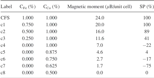
Finally, we discuss how the chemical changes at the interface affect the magnetic and electronic properties of this region. Due to the presence of inter-diffusion, it is to be expected that the interface region will show decreased per-formance. In order to reveal the influence of the local inter-face atomic structure on the magnetic moment and spin-polarization, we performed DFT calculations for the eight configurations shown in Table I. Besides the intermixing at the interface, the overall cubic structure of the film at the very interface has not been altered (supplementary Fig. S424). Hence, all considered configurations have CFAS type lattice, but with altered chemical composition.
The interface region is continuously changing from Si to CoSix-rich and finally to the full CFAS structure. Starting
from Co2FeSi (CFS) (Al has been omitted due to very low
Al presence at the interface), we gradually replace Fe atoms with Si in the conventional CFS cell. Therefore, four such configurations are constructed and labelled asc1,c2,c3, and
c4, with chemical compositions shown in TableI. The table shows that the magnetic moment gradually decreases from 24lB per unit cell in CFS to 7.0lB per unit cell in thec4
configuration. In addition, decrease in Co concentration will further decrease the magnetic moment, and for thec8 config-uration, which is stoichiometric CoSi2structure, it becomes
equal to zero. It is worth noting that the CoSi2structure is a
silicide compound that has a Heusler like cubic structure. The gradual decrease of the magnetization across the inter-face was also confirmed by polarised neutron reflectivity measurements, not presented here. The spin-polarization also shows a decreasing trend as illustrated by the spin-polarised DOS for several selected configurations compared to the DOS for the fully ordered CFS structure (supplementary Fig. S524). The values for the spin-polarization at Fermi level for all considered configurations are presented in TableI.
In summary, we have shown that the CFAS film depos-ited on Si(111) has a single crystalB2 structure with twin
related epitaxial relationship with the substrate. Sub-nanometre EELS showed that at the interface there is a mu-tual inter-diffusion among Si, Fe, and Co over a 3 nm region. The analysis shows that this narrow interface region is Si rich and dominated by the presence of CoSix phases. This
indicates that Si is mainly substituting Fe which was further supported by performing first-principles calculations. Over the same region, due to the out-diffused Si, there is a very low presence of Al. Atomic resolution aberration corrected electron microscopy showed that the inter-diffusion is of substitutional nature. This allows creation of realistic models of the interface structure, used to perform first principles cal-culations in order to provide insight into how the altered chemical composition modifies the local electronic and mag-netic properties. The calculations showed that the increased Si incorporation in the film leads to decrease in the magnetic moment and significant reduction of spin-polarization at the Fermi level. These effects can have significant detrimental role on the spin injection from CFAS into Si, besides the structural integrity of this junction. Therefore, these phenom-ena of intermixing, even though they are limited to very nar-row interface region, have to be addressed in order to fully exploit the 100% spin polarization of the CFAS electrode.
This work was funded by the Engineering and Physical Sciences Research Council (EPSRC) through Grant Nos. EP/ K03278X/1 and EP/K032852/1. The SuperSTEM Laboratory is the U.K. National Facility for Aberration-Corrected STEM, supported by the EPSRC.
1
R. A. de Groot, F. M. Mueller, P. G. v. Engen, and K. H. J. Buschow, Phys. Rev. Lett.50, 2024 (1983).
2
B. Balke, S. Wurmehl, G. H. Fecher, C. Felser, and J. K€ubler, Sci. Technol. Adv. Mater.9, 014102 (2008).
3
S. Wurmehl, G. H. Fecher, H. C. Kandpal, V. Ksenofontov, C. Felser, H.-J. Lin, and H.-J. Morais,Phys. Rev. B72, 184434 (2005).
4
A. Hirohata, J. Sagar, L. Lari, L. R. Fleet, and V. K. Lazarov,Appl. Phys. A111, 423 (2013).
5C. Felser, G. H. Fecher, and B. Balke,Angew. Chem., Int. Ed.46, 668
(2007).
6N. Tezuka, N. Ikeda, S. Sugimoto, and K. Inomata,Appl. Phys. Lett.89,
252508 (2006).
7R. Farshchi and M. Ramsteiner,J. Appl. Phys.113, 191101 (2013). 8
H. Dery, P. Dalal, L. Cywinski, and L. J. Sham,Nature447, 573 (2007). 9
T. Tomoyasu, W. Eiji, I. Mitsuru, and Y. Masahito,NPG Asia Mater.3, 65 (2011).
10
K. Kasahara, Y. Fujita, S. Yamada, K. Sawano, M. Miyao, and K. Hamaya,Appl. Phys. Express7, 033002 (2014).
11
Y. Fujita, S. Yamada, Y. Maeda, M. Miyao, and K. Hamaya,Thin Solid Films557, 386 (2014).
12
K. Tanikawa, S. Oki, S. Yamada, M. Kawano, M. Miyao, and K. Hamaya, Thin Solid Films557, 390 (2014).
13
M. Kawano, S. Yamada, S. Oki, K. Tanikawa, M. Miyao, and K. Hamaya, Jpn. J. Appl. Phys., Part 152, 04CM06 (2013).
14
A. Fert and H. Jaffre`s,Phys. Rev. B64, 184420 (2001). 15
S. Yamada, K. Tanikawa, S. Oki, M. Kawano, M. Miyao, and K. Hamaya, Appl. Phys. Lett.105, 071601 (2014).
16
T. Hentschel, B. Jenichen, A. Trampert, and J. Herfort,J. Phys. D: Appl. Phys.45, 055002 (2012).
17
S. Oki, S. Yamada, T. Murakami, M. Miyao, and K. Hamaya,Thin Solid Films520, 3419 (2012).
18
L. Lari, S. Lea, C. Feeser, B. W. Wessels, and V. K. Lazarov,J. Appl. Phys.111, 07C311 (2012).
19
C. T. Koch, Ph.D. thesis, Arizona State University, 2002. 20
S. J. Clark, M. D. Segall, C. J. Pickard, P. J. Hasnip, M. I. J. Probert, K. Refson, and M. C. Payne,Z. Kristallogr.220, 567 (2005).
TABLE I. Influence of structural disorder on the magnetic moment and spin-polarization at the Fermi level. The CFS conventional 16 atoms cubic unit cell is chosen as reference. CFeand CCorefer to the relative (compared to the number of atoms in the CFS unit cell) number of atoms per unit cell.
Label CFe(%) CCo(%) Magnetic moment (lB/unit cell) SP (%)
CFS 1.000 1.000 24.0 100
c1 0.750 1.000 20.0 100
c2 0.500 1.000 16.0 89
c3 0.250 1.000 11.6 41
c4 0.000 1.000 7.0 22
c5 0.000 0.875 4.6 4
c6 0.000 0.750 2.7 17
c7 0.000 0.625 1.7 75
c8 0.000 0.500 0.0 0
[image:5.612.50.297.642.767.2]21S. Chadov, G. H. Fecher, C. Felser, J. Minar, J. Braun, and H. Ebert,
J. Phys. D: Appl. Phys.42, 084002 (2009). 22
P. J. Hasnip, J. H. Smith, and V. K. Lazarov,J. Appl. Phys.113, 17B106 (2013). 23A. J. Morris, R. J. Nicholls, C. J. Pickard, and J. R. Yates,OptaDOS: User Guide Version 1.0(University of Cambridge, University of Oxford and University College London, 2013).
24See supplementary material athttp://dx.doi.org/10.1063/1.4948466for
fur-ther structural characterization as well as spin-polarized DOS plots for sev-eral selected configurations at the interface.
25P. J. Hasnip, C. H. Loach, J. H. Smith, M. I. J. Probert, D. Gilks, J.
![FIG. 1. (a) Low magnification HAADFSTEM image showing an overview andconfirming the thickness uniformity ofthe CFAS film; (b) SAD taken alongthe [1–10] zone axis from an area cov-ering both the film and substrate](https://thumb-us.123doks.com/thumbv2/123dok_us/7857236.179312/3.612.52.406.595.767/magnication-haadfstem-overview-andconrming-thickness-uniformity-alongthe-substrate.webp)
![FIG. 2. (a) HAADF STEM image showing the structural ordering of theCFAS film viewed along the [1–10] zone axis, with overlaid structuralmodel](https://thumb-us.123doks.com/thumbv2/123dok_us/7857236.179312/4.612.60.290.52.368/haadf-showing-structural-ordering-thecfas-viewed-overlaid-structuralmodel.webp)