b
Department of Electronics and Computer Science, University of Southampton, Highfield, Southampton, UK
Abstract
We report simulations and experimental work relating to innovations in the area of ultra short channel vertical transistors. The use of dielectric pockets can mitigate short channel effects of charge sharing and bulk punch-through; thickened oxide regions can minimize parasitic overlap capacitance in source and drain; a narrow band gap, SiGe source can reduce considerably the gain of the parasitic bipolar transistor which is particularly severe in vertical MOSFETs. The work is put into the context of the ITRS roadmap and it is demonstrated that vertical transistors can provide high performance at relaxed lithographic constraints.
Ó 2004 Elsevier B.V. All rights reserved.
1. Introduction
The continued scaling of MOSFETs to the deca-nanometre regime presents very major tech-nological challenges to the industry and will
re-quire enormous investment in plant and
equipment. Vertical transistors are currently of interest because they offer a route to ultra-short channel MOSFETs with relaxed (that is cheap) lithography rules. In addition, such transistors have much reduced footprint: up to a factor of 2.4 has been described [1]. Particular issues for vertical MOSFETs compared to their conventional lateral counterparts, are the higher overlap capacitance, high current drive and high gain parasitic bipolar
transistor (PBT) and problems with channel engi-neering to control short channel effects (SCE). We describe in this paper, our recent work which ad-dresses these short-comings of vertical transistors. Fig. 1 shows a schematic diagram that serves to summarise some of the architectural features that we propose. Notice that the transistor can be considered to operate in either source up, or down modes although not all architectural features are appropriate for bi-directional operation. Specifi-cally we identify the use of a so-called dielectric pocket (DP) to control SCE (source down mode) [2,3], thickened oxide regions, including a novel fillet oxidation (FILOX) overlap process to mini-mize overlap capacitance [2,4] and the use of poly-SiGe regions to reduce the emitter efficiency of the PBT (source up mode) [5]. We now consider these concepts, and indicate the expected performance advantage in the ITRS context. Furthermore, ex-perimental results are presented on single- and *
Corresponding author. Tel.: 151-794-4529; fax: +44-151-794-4540.
E-mail address:[email protected](S. Hall).
surround-gate vertical MOSFETs [6]. Reduced overlap capacitance is demonstrated due to birdÕs beak formation in the FILOX process. It should be noted that our approach is to realize transistors that can be integrated into a CMOS process.
[image:2.544.286.492.91.304.2]2. Short channel effects
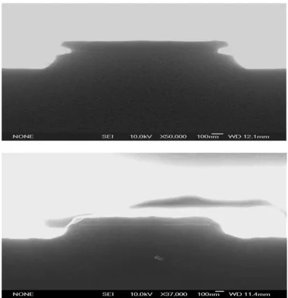
Fig. 1 shows the incorporation of a thin oxide region (DP) on top of a pillar which defines the vertical transistor. The channel is formed by growth of a thin epitaxial layer after etching the pillar using a scheme similar to that of a graft base in heterojunction bipolar processing. We show in Fig. 2 SEM cross sections illustrating the recessed DP. This strategy permits adequate seeding of the epitaxial layer and so overgrowth to ensure con-nectivity over the edge of the DP region. The DP serves a number of roles: it prevents dopant out-diffusion and so mitigates bulk punch-through ef-fects, it influences the electrostatics of the drain region so reducing charge sharing and finally, ef-fectively suppresses the PBT associated with source/body/drain regions. Fig. 3 shows ISE sim-ulation results which summarise the on- and off-current for different body doping and contact width for a verticalp-MOSFET. The influence of the DP is such thatIOFF can be reduced with little
reduction inION. The reduction inIONis a result of
the reduced charge sharing and hence increasedVT
whereas theIOFF reduces due to suppressed DIBL
and punch-through. For WC¼50 nm, the DP no
longer influences the electrostatics at the drain. A body doping of 21018 cm3, W
C¼25 nm,
tOX¼2 nm, gives VT¼ 0:28 V and IOFF ¼1:5
nA/lm atVDD¼1 V.
3. Reduction of parasitic overlap capacitance
[image:2.544.49.252.94.208.2]Parasitic capacitance represents probably the biggest challenge for vertical MOSFETs. The strategy here is to look for ways of thickening oxide regions, as depicted in Fig. 1. Reduction of gate-source overlap capacitance (bottom of pillar) is achieved by a LOCOS type processÔFILOXÕ[3]. Fig. 4 shows a field emission SEM cross-section of
Fig. 1. Vertical MOSFET schematic.
Fig. 2. SEM before and after epi-channel growth.
[image:2.544.286.492.348.474.2]a vertical n-MOSFET featuring this approach. Incorporation of a deposited oxide region on top of the pillar and the thicker oxide grown on the highly doped poly-Si extrinsic drain contact can reduce significantly the gate-drain capacitance. A study using MOS-capacitors has demonstrated a 5-fold reduction in parasitic overlap capacitance using FILOX and a thick top oxide [3]. To sum-marise the study, we show in Fig. 5,C–Vplots for pillars with gate oxide only, with a 20 nm thermal oxide–130 nm CVD nitride and 50 nm LTO stack (ONO) and finally the ONO stack plus the FILOX process. The ONO stack reduces the capacitance by 30% and the introduction of the FILOX gives the reduction overall of a factor 5. A
semi-fall time is used to quantify the delay of the in-verter and the influence of each parasitic compo-nent can be considered in turn. Fig. 1 includes the results of such a study whereby the required rela-tive thicknesses of the thickened oxide regions are noted. Fig. 6 shows the performance of the opti-mised device in the context of the ITRS roadmap. Note that the channel length of the vertical MOSFET remains fixed at 50 nm. The device shows considerably advantage over its lateral counterpart for technology nodes down to 90 nm. The degradation of performance thereafter arises because of the scaling of the supply voltage. The effect of maintaining aVDDof 1 V is shown also. It
[image:3.544.55.255.92.238.2]should be noted that interconnect capacitance will become dominant at lower technology nodes where the additional drive offered by the vertical MOSFET dual channels will offer further advan-tage. This is demonstrated in the figure by the in-clusion of a fixed load of 5fF and the vertical MOSFET is seen to competitive down to 50 nm. The source and drain resistances of the vertical MOSFET (extracted from ISE simulation) are 3–4
[image:3.544.68.241.477.648.2] [image:3.544.294.490.501.648.2]times smaller than the ITRS values and these re-sistances do not significantly increase when the device is scaled as shown in Fig. 7. This arises es-sentially because the dielectric pocket precludes the need for pockets or extensions.
4. Experimental transistor characteristics
Both p-channel and n-channel test transistors have been successfully fabricated to demonstrate some of the concepts outlined above. Gate oxide thickness was 3 nm. Single, double and surround gate types have been realised and Fig. 8 shows the gate over-drive ION versus drawn width W, for
each type. The expected linear relationship is seen for each type confirming full control of the chan-nel. Process differences account for the
[image:4.544.288.489.91.245.2]non-convergence of the data of each type. Fig. 9 shows transfer characteristics of a double gate n -MOS-FET with W ¼9lm and L¼125 nm for both
[image:4.544.48.255.95.218.2]Fig. 7. Scaling of series resistance.
[image:4.544.288.489.318.647.2]Fig. 8.IONversusW for each vertical MOSFET type.
Fig. 9.I–V plots for double gaten-MOSFETs.
[image:4.544.52.250.490.647.2]both source and drain contacts. Sheet resistance of 49 X= has been extracted from experimental
devices.
5. Suppression of parasitic bipolar transistor
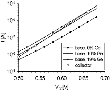
The dielectric pocket concept brings the added benefit of reducing considerably the area of the effective emitter and collector formed by the source and drain of the vertical MOSFET and so reduced the magnitude of base and collector currents of the PBT. The DP device is however inherently Ôdrain upÕ. An alternative approach to minimise parasitic bipolar transistor gain for drain-down configura-tions (source at the top), is to include a poly-SiGe extrinsic source contact [5]. This serves to steepen the profile of minority carriers injected into the parasitic emitter so increasing the base current and reducing the gain. A theoretical model for the base current of such a polySiGe emitter has been de-veloped, which combines the effects of the poly-SiGe grains, the grain boundaries and the interfacial layer at the polySiGe/Si interface into an expression for the effective surface recombina-tion velocity of a polySiGe emitter [5]. The model is equally valid for the parasitic BJT in vertical MOSFETs. Silicon bipolar transistors were fabri-cated with 0, 10% and 19% Ge in the polySiGe emitter and the variation of base current with Ge content characterised. Fig. 11 shows Gummel plots from bipolar test transistors where a con-siderable reduction in BJT gain is evident. The measured base current for a polySiGe emitter is seen to increase by a factor of 3.2 for 10% Ge and 4.0 for 19% Ge compared with a control transistor containing no germanium, in good agreement with the theoretical predictions. The competing mech-anisms of base current increase by Ge
incorpora-tion into the polysilicon and base current decrease due to an interfacial oxide layer were investigated. The size of the base current increase with Ge content depends on the thickness of the interfacial layer, with larger increases being obtained for thinner interfacial layers. The introduction of germanium into a polysilicon emitter therefore allows the base current, and hence the gain, to be controlled by means of the Ge content in the polySiGe parasitic emitter of a vertical MOSFET.
6. Discussion and conclusions
We have reviewed in this paper, a number of strategies to address problems with realising high performance vertical MOSFETs. Our transistor architectures and processes are all compatible with full CMOS realisation. We have demonstrated by simulation that a dielectric pocket can reduce charge sharing and other short channel effects to produce a transistor with goodIONtoIOFFratio. It
[image:5.544.301.487.91.246.2]is worth noting that the approach has a particular benefit for thep-MOSFET in that excessive boron penetration in the bulk of the transistor is pre-vented. A process to realise the DP has been de-veloped based on that of a HBT graft base. Continuity of the epitaxial channel layer over the DP edge has been achieved. Strategies to reduce parasitic capacitances have been proven and shown to produce a factor of five improvement from capacitors. A LOCOS type, FILOX process
has been developed to place a thick oxide in the bottom contact region of the device to reduce greatly the overlap capacitance. A semi-analytical circuit based model has been developed to identify the important parasitic overlap capacitance com-ponents and to assist in the optimisation of the device. The semi-optimised device performance has been assessed in the context of the ITRS roadmap. The reduced scaling constraints for channel length and series resistance suggest great potential for these transistors. Experimental test transistors have been successfully realised. A nar-row band gap concept to suppress parasitic tran-sistor action in the vertical MOSFETs has been shown to reduce the gain by a factor of three.
Acknowledgements
The authors acknowledge the support of the SIGMOS project of the European Commission
and the UK funding body EPSRC under Grant GRM93178.
References
[1] T. Schulz, W. Roesner, L. Risch, A. Korbel, U. Langmann, IEEE Trans. Electron. Dev. 48 (8) (2001) 178–183.
[2] D. Donaghy, S. Hall, V.D. Kunz, C.H. de Groot, P. Ashburn, Proc. ESSDERC (2002) 499–502.
[3] M. Jurczak, T. Skotniki, R. Gwoziecki, M. Paoli, B. Tormen, P. Ribot, D. Dutartre, S. Monfay, J. Galvier, IEEE Trans. Electron. Dev. 48 (8) (2001) 1770–1774.
[4] V.D. Kunz, T. Uchino, C.H. de Groot, P. Ashburn, D.C. Donaghy, S. Hall, Y. Wang, P.L.F. Hemment, IEEE Trans. Electron. Dev. 50 (6) (2003) 1487–1493.
[5] V.D. Kunz, C.H. de Groot, S. Hall, P. Ashburn, IEEE Trans. Electron. Dev. 50 (6) (2003) 1480–1486.