Low Voltage Power Conversion
Marshall Howard Shepard
A thesis submitted for the degree of Master of Philosophy of The Australian National University.
Declaration
I certify that, except where otherwise acknowledged in the text, this thesis is entirely my own work. I further certify that it contains no material previously submitted for a degree of The Australian National University, or of any other university or tertiary institution.
Abstract
This thesis describes the design, construction and evaluation of a DC-DC converter intended for use with very low input voltages, such as would be obtained from a single solar cell or a parallel solar array. Although the low voltage power converter discussed here has been optimised for inputs from 0.5 to 0.6VDC, operation down to 0.3V or less is practical.
Particular importance is placed on the design of magnetic components. A new, semi-passive technique for the control of staircase saturation in transformer cores is
presented. Unfortunately, the technique has proven to be unsuitable for low voltage applications. The reasons for this are explained.
A circuit model for the converter is developed, and used to predict circuit operation. A core flux displacement hypothesis is presented, which addresses a discrepancy in voltage transfonnation between measured data and the model. To test the hypothesis, a specially constructed nickel steel transformer core was installed and evaluated.
Table of Contents
Abstract.
Table of Contents List of Acronyn1s. Photographs .
1 Introduction .
1.1 Obtaining useful power from a PV array 1.2 Low voltage power conversion
1.3 The 500A DC Power Supply 1.4 Thesis overview
2 Theory
2.1 The PV cell to DC converter interface
2.2 Overview of competing converter technologies 2.3 Transfonner 1nagnetics, detailed model
2.4 Core saturation, cause and prevention 3 L VPC Design .
3 .1 Introduction
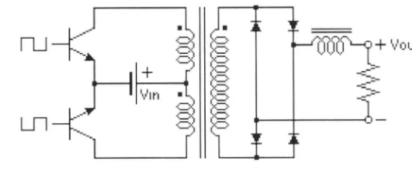
3 .2 The push-pull converter
3 .3 MOSFET drive circuit and snubber 3 .4 Drive circuit power supply
3. 5 Transformer design
3. 6 Leakage inductance minimisation 3. 7 Antisaturation feature
3.8 Inductive output clamp and filter L VPC sche1natic diagram
4 DC Power Supply Design 4.1 Introduction
4.2 Fast settling, high current linear regulator 4.3 Parasitic inductance
4.4 The1mal management
4.5 Photovoltaic array equivalence
3 4 6 7 8
13
. 29
5 Results
5.1 LVPC operating characteristics 5 .2 Transformer characterisation 5.3 Core saturation
5.4 Antisaturation feature
5.5 Operating li1nitations and fault/overload tolerance 5.6 DCPS operating characteristics
6 Modelling
6.1 Introduction 6.2 Circuit ele1nents
6.3 Equivalent circuit equation 6.4 Model evaluation
7 Discussion .
7 .1 Interpretation of results 7 .2 Measurement error analysis 7. 3 Design improvements
7. 4 Co1n1nercial potential 8 Nickel Steel Core
8 .1 Introduction
8.2
Eddy current reduction8.3
L and Lp measurement 8.4 Imag, Bmax and µr8.5 Core losses 8.6 Test results
8.7 Drive frequency reduction 8.8 "Missing" voltage
8.9 Dependence of Vioss upon Iin 9 Conclusions .
References .
Acknowledgments
Appendix I - List of Materials, L VPC. Appendix II - List of Materials, DCPS
Appendix III - Transformer Primary and Supply/Drain Bars
55
. 74
84
. 93
108
110
Acronyms
AC ANU CGS CSES DC DCPS DMM EMF ESR FEIT FET GBWP LCR LED
Alternating Current
Australian National University Centimetre Gram Second
Centre for Sustainable Energy Systems Direct Current
Direct Current Power Supply Digital Multimeter
Electromotive Force
Equivalent Series Resistance
Faculty of Engineering and Information Technology Field Effect Transistor
Gain Bandwidth Product
Inductance (L) Capacitance (C) Resistance (R) Light Emitting Diode
L VPC Low Voltage Power Converter MKS Metre Kilogram Second
MOSFET Metal Oxide Silicon Field Effect Transistor NiFe Nickel Steel
PCB Printed Circuit Board PV Photovoltaic
RMS Root of the Mean of the Squares SS Stainless Steel
Low Voltage Power Converter
1 Introduction
1.1 Obtaining useful power from a photovoltaic array
Silicon solar cells produce DC electric power most efficiently when their output is approximately 0.6V per cell. Because this voltage is relatively low, cells are usually connected in series to form an array. For some applications ( charging batteries,
operating remote bore pumps) the power fro1n DC solar arrays may be used directly. However, it is often desirable to convert the DC output to AC at some convenient
voltage ( e.g. 240Vrms ). Electronic devices ("inverters") which convert DC to AC are commonly available and can take many forms. Most inverters require an input of at least 12VDC, and therefore at least 20 solar cells must be connected in series to obtain the necessary voltage. In stand-alone systems where power may be required in the
absence of sunlight, solar cells charge batteries which in tum supply DC-DC converters or DC-AC inverters.
1.2 Low voltage power conversion
High efficiency solar cells and sun tracking solar concentrator arrays have been the
subject of intense research interest within the FEIT Department of Engineering for many years. Significant progress has been made, both in the efficiency of photovoltaic cells and in the performance of the optical concentration systems in which they are used.
Although much progress has been made in improving cells and concentrators, the
electrical power conversion techniques used to transform the output from these arrays have heretofore relied on DC converter or inverter circuits designed for inputs of 12V to 48V or more. Off-the-shelf power conversion products for use with low and extra low input voltages have not been available. This restriction has led to the necessity of
defective cells can be reduced through the use of bypass diodes, but they dissipate power and can be difficult to install. Because cell anodes must be electrically isolated from each other, series arrays also impose limitations on thermal resistance between the
cells and the heatsink.
Parallel arrays offer advantages in that all anodes can be bonded to a common heatsink, which can also serve as the positive output connection. Cell matching, solar tracking and uniformity of illumination become less critical; even a totally blocked cell has little overall effect. The disadvantage of parallel arrays is that output current will be one or two orders of 1nagnitude greater than that which exists in a series array of
equivalent output. As most electrical power conversion techniques rely on current switching, the ability to produce an economical low resistance switch is crucial to the success of low input voltage converters. (Shepard and Williamson [ 12]).
Previous work in the area of low voltage power conversion appears to be limited. Meyer and Schmidt [10] describe a lOW DC-DC converter operating fro1n a 0.7V input and a 250W converter for use at 1.4V. The first was designed for fuel cell applications while the second was developed for three-junction amorphous silicon solar cells.
Efficiencies of 80 to 95o/o were reported, but few details of the design were given.
The DC-DC converter discussed in this thesis is designed to operate from a parallel solar concentrator array with an output of about 0.55VDC at 450A. The circuit should convert this to 25VDC at 8A, suitable for charging batteries or operating a conventional 1nains output inve1ier. The 200W power level was selected because it is high enough to
give a true feeling for the proble1ns involved, yet low enough to be achieved within a lin1ited ( ~$5,000) budget.
Extracting useful power from SOOADC at
Y2
V potential is analogous to extracting the same power (250W) from a 500 litre/second flow of water at 5cm head. Both are mathematically easy, but both are technically challenging. The energy density of these sources is quite low (Yi J/C and Yi J/1, respectively), therefore large flows must be acco1nmodated to produce the required power. This leads to physically large (andA low impedance source demands a low impedance transducer, if reasonable efficiency
is to be achieved.
There are also control problems associated with such high flow rates. Imagine
instantly closing a valve in a length of pipe carrying a flow of 500 1/s. Not only would it be difficult to close a large valve "instantly", but unless they were very strong, the
inertia of the water could cause the valve or pipe to rupture. Continuing with the
analogy, if the cormnutation transistors in the 12V converter turn off in 0.5µs, even the inductance of 10cm of wire could convert the "inertia" of 500A (through ""0.1 µH) into a
100V spike.
Identifying and analysing problems of particular relevance to low energy density electrical power conversion was a primary objective of this project. The second main goal was the construction of an efficient working prototype.
1.3 The SOOA DC Power Supply
It is not convenient to use a solar concentrator array as a power source for developing prototype DC-DC converters. There are several reasons for this: It is sometimes
necessary to work on cloudy days. A parallel concentrator array is not currently
available and, even if one was, no physically realisable cable could carry the necessary cun·ent from the array to the laboratory without incurring an unacceptable voltage loss. (In practice, it would almost certainly be necessary to locate a low voltage converter very close to the solar array.) Therefore, a power supply is required which is capable of si1nulating the output of a 250W parallel solar array.
1.4 Thesis overview
This thesis begins (Section 2) with a discussion of the technologies relevant to the production of "useful" DC voltages ( e.g. 24V) from the output of a parallel array of solar cells. Topics include the characterisation of the photovoltaic effect in silicon, the relative 1nerits of various DC-DC converter configurations, and the magnetics of
transfonner design.
The next two sections (3 and 4) reveal the steps involved in the design and
construction of a Low Voltage Power Converter (L VPC) and a 500A DC Power Supply. At each stage, design decisions are highlighted and justified. Particular attention is paid to the design of magnetic components - the L VPC transformer and output inductor. The operation of both circuits is discussed in some detail. These two pieces of equipment fonned the basis of the experimental part of the project.
Results gained from perfonnance testing of the LVPC and DC Power Supply are
presented in Section 5. LVPC circuit losses are analysed in ( excruciating) detail, and a con1plete 1nodel of its transformer is developed. Performance specifications are
presented for both the LVPC and DC Power Supply, together with an analysis of their operating li1nitations and potential failure modes.
A circuit model for the L VPC is developed in Section 6. Simplifying assumptions are made, permitting the adoption of a DC equivalent circuit. The contribution of each
element or functional block within the circuit is analysed, and the effects are
incorporated in the model. Predictions based on this model are then compared with actual results, and similarities and discrepancies are noted.
Section 8 describes the design and characterisation of the L VPC transformer utilising a replacement core of laminated nickel steel. Revised performance figures are provided,
conclusions are drawn, and some remaining questions are discussed. The section
concludes with a discussion of an as-yet unresolved question concerning a voltage loss observed at the transformer secondary during all stages of the project. In this context, a moderately non-linear dependence of voltage loss on input current is explored.
Following is a summary of the principal findings, concepts and contributions resulting fro1n this project:
• Notwithstanding the inherent difficulties, the output of a parallel photovoltaic array can be efficiently and reliably converted to a more useful voltage.
• Stray inductance and transformer leakage inductance are principal limiting factors in the design of efficient low voltage DC-DC converters.
• Stray inductance and the commutation of large currents dictate that snubber circuits be used on high power switching supplies - even when the source voltage is low. • An inductive output filter can significantly improve the performance of forward
converters, particularly when leakage inductance is present.
• Contact resistance and skin effect can be significant sources of loss in high current low voltage AC circuits, even at relatively low frequencies.
• Constructing a O. lmO switch capable of changing state in 0.5µs is electrically si1nple, aesthetically pleasing, mechanically difficult, and financially painful.
• Power ferrites can be used to advantage at frequencies as low as lkHz, particularly in circumstances where the higher flux density and permeability of steel alloys cannot be fully utilised due to other constraints.
• It should be possible to control staircase saturation in a transformer core by briefly
2 Theory
2.1 The PV cell to DC converter interface
A silicon solar cell is simply a p-n junction designed to maximise electrical output power when exposed to sunlight. As a first order approximation, it may be represented
as a diode in parallel with an ideal current source. The current source results from the
separation of hole/electron pairs at the junction in response to the absorption of photons. The resulting current/voltage characteristics are therefore those of an ideal diode
forward biased by a light dependent current source. For the purposes of this discussion, the series resistance introduced by metallic contacts and bulk silicon must also be
considered.
The expression governing the I/V characteristics of a silicon diode is
V r = (nkT/q) ln(Ir/10) [2- 1]
where V f is the forward junction voltage, n is a current dependent factor of about 1 at higher current densities (Grove [6], pp. 186-190), k is Boltzmann's constant, Tis
absolute te111perature, q is the charge of an electron, If is the forward junction current, and I0 is the junction reverse saturation current.
Solar cells produced by the ANU Centre for Sustainable Energy Systems are
designed to operate at 20 suns, or an incident solar flux of about 2.0 W/cm2. Even with
active liquid cooling, junction temperatures of around 60°C can be expected (Andrew
Blakers, pers. comm.). Under these conditions, cells typically have an open circuit voltage of 680m V and produce a short circuit current of 700mA/cm2 (Andrew Blakers,
Andres Cuevas and William Keogh, pers. comm.).
Because a cell is equivalent to a diode in parallel with a current source, an open
circuited 1 cm2 cell with 2.0 W/cm2 solar spectrum illumination will have 680m V
1 - 11
0.680 = 0.0287 n(0.700/I0) , or I0 = 3.591 xlO A. [2-2]
Therefore, for the cells in question,
- 11) - 11
Yr= 0.0287 ln(Ir/3.591 xlO , or If= 3.591xlO exp(34.84Vf). [2- 3]
If If is the junction current, then 0.700 - If will be the cell output current, lout·
Vf is the voltage at the p-n junction, not the cell output voltage. Thin metal fingers on the upper surface of each cell are used to make electrical contact with then-type silicon cathode. Junction current must also pass through the relatively thick p-type silicon
substrate which forms the anode. The combined resistance associ~ted with the fingers and substrate would be about 0.0030 for a typical 18A cell (Keogh, pers. comm.).
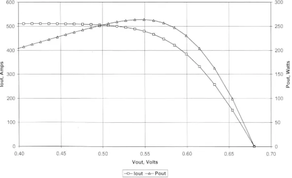
Normalising this figure on a per-square-centimetre basis gives 0.003 x 18/0. 7 = 0.0770. This resistance, Rs, is in series with If, and will produce voltage drop Vs. The actual cell output voltage, Y out, will be reduced by this amount. Cell output power, Pout = Y out x lout, and efficiency can be computed from P ou/2.0. Figure 2.1 summarises these results. The full set of calculated data from which this figure was derived appears in Table 2.1.
1/) a. E <t: ... -::i ..2
0.8
0.7
0.6
0.5
0.4
0.3
0.2
0.1
0.0
~
; - - - j - - - t - - - + - - - + - - -~ - - - - + - - - ---+ 12
>-rt=
UJ + - - - t - - - t - - - + - - - + - - - _ _ _ _ _ : , , A - - l - - - - ---1-9
+ -- - - + - - - + - - - + - - - + - - - +~ - - ---1-6
, - - - t - - - t - - - + - - - + - - - + - ~ - - - - l - 3
-j-- -- - - j- - - ---t-- - - + - - - + - - - - ---+- - - - b ----1-, 0
0.40 0.45 0.50 0.55 Vout, Volts
0.60 0.65 0.70
[image:14.787.135.721.670.1030.2]i
--0-
lout -tr-Eff'y ITable 2.1 Characteristics of ANU CSES Solar Cells at 20 Suns (2.0W/cm2).
Vf If lout Rs Vs Vout Pout
0.45 0.000 0.700 0.077 0.054 0.396 0.277
0.46 0.000 0.700 0.077 0.054 0.406 0.284
0.47 0.000 0.700 0.077 0.054 0.416 0.291
0.48 0.001 0.699 0.077 0.054 0.426 0.298
0.49 0.001 0.699 0.077 0.054 0.436 0.305
0.50 0.001 0.699 0.077 0.054 0.446 0.312
0.51 0.002 0.698 0.077 0.054 0.456 0.319
0.52 0.003 0.697 0.077 0.054 0.466 0.325
0.53 0.004 0.696 0.077 0.054 0.476 0.332 0.54 0.005 0.695 0.077 0.053 0.487 0.338 0.55 0.008 0.692 0.077 0.053 0.497 0.344 0.56 0.011 0.689 0.077 0.053 0.507 0.349 0.57 0.015 0.685 0.077 0.053 0.517 0.354 0.58 0.021 0.679 0.077 0.052 0.528 0.358 0.59 0.030 0.670 0.077 0.052 0.538 0.361
0.60 0.043 0.657 0.077 0.051 0.549 0.361
0.61 0.061 0.639 0.077 0.049 0.561 0.358 0.62 0.086 0.614 0.077 0.047 0.573 0.351 0.63 0.122 0.578 0.077 0.044 0.586 0.338 0.64 0.173 0.527 0.077 0.041 0.599 0.316 0.65 0.246 0.454 0.077 0.035 0.615 0.279 0.66 0.348 0.352 0.077 0.027 0.633 0.223 0.67 0.493 0.207 0.077 0.016 0.654 0.135 0.68 0.699 0.001 0.077 0.000 0.680 0.001
Vf= Cell forward bias junction voltage. Vf= 0.0287 ln(lf!3.591 xl0-11).
lf
= Cell forward bias junction current, in Amperes.h
= 3.591x10⁻¹¹ exp(34.84V f). lout= Cell output current, in Amperes. lout= 0. 700 -lf.
Rs = Cell contact finger plus substrate resistance, in Ohms. Vs= Voltage drop across Rs. Vs= lout x Rs.
Vout = Cell output voltage. Vout = V f - Vs·
pout = Cell output power, in Watts. pout = Vout X lout•
Eff'y = Cell efficiency, in percent. Eff'y = 1 OOP out/2.0.
Eff'y
13.86 14.21 14.56 14.90 15.25 15.59 15.93 16.26 16.58 16.90 17.20 17.47 17.71 17.91 18.03 18.05 17.92 17.57 16.91 15.78 13.97 11.14 6.77 0.05
Cell efficiency is highest (18°/o) when Vout = 0.55V, but remains above 17% from about 0.49 to 0.58V. To achieve maximum overall efficiency, the power converter
should be designed to operate with an input voltage within this range ( or, in the case of a series array, a 1nultiple of it). This window of optimum efficiency will change
[image:15.787.117.736.141.657.2]accommodate a± 10°/o change in operating voltage without reducing overall efficiency by 1nore than 6% of its maximum value.
It should be noted that at voltages below the optimum power point the cell tends to look like a current source, while above this point it looks like a voltage source. Because of this, the converter designer must ensure current draw is relatively steady, otherwise cell voltage, and therefore efficiency, will vary. On the other hand, design is simplified to so1ne extent because cells can produce neither excessive current under short circuit conditions, nor excessive voltage under no-load conditions.
2.2 Overview of competing converter technologies
Electrical power conversion can be defined as the process by which one form of elect1ical energy is transformed into another. The start and end points can be AC, DC, or a co1nbination of both, and the conversion process can be either electrical or
electron1echanical. As this project is concerned primarily with the conversion of DC power from silicon solar cells, only DC input converters will be considered.
Electro1nechanical conversion is usually implemented with some form of
n1otor/generator or 1notor/alternator combination, although these may share a single mechanical structure. DC input motor/alternators can convert the output of solar cell an·ays directly into mains power with reasonable efficiency (70-80o/o). Their principal disadvantages of size, weight and maintenance requirements are partially offset by their chief advantage: robustness. (Iron withstands lightning better than electronic circuitry.)
Almost all forms of DC electrical power conversion require some form of
commutation. Therefore, an alternating voltage or current is always present within the
device. The reason for this is simple: The 1nagnetic components which function as
energy storage and transfer elements depend upon changing magnetic fields for their
operation, and DC can only produce a constant magnetic field. (The ho1nopolar
n1otor/ generator is an exception. It sidesteps the co1nmutation requirement by using sliding DC contacts and a fixed 1nagnetic field.)
Electronic power converters can be designed to produce either AC or DC outputs.
However, if a sinusoidal mains voltage output is desired, the conversion is usually
accomplished in two stages. The input DC voltage is initially converted to another
(usually higher) DC level, which then feeds a DC to AC inverter. Mains output DC-AC
inve1iers with inputs fro1n 12 to 96V are co1nmonly available. For this reason, it was
decided that a low input voltage DC-DC converter stage would be the primary focus of
this investigation.
Most electrical DC-DC converters fall into one of two broad categories. The first is
theflyback converter (figure 2.2), in which energy at one voltage or current is
temporarily stored in an inductive circuit element, to be subsequently retrieved at a
second voltage or current. In the flyback converter, energy storage takes place while the
co1nmutating device is conducting. This energy is then transferred to the load while the
commutating device is switched off. Stored magnetic energy is fundamental to device
operation, while turns ratio (in those cases where a transformer forms the energy storage
element) is of lesser importance, as it does not determine the voltage transfer ratio of the
converter. If a transformer is used, its principal function is to provide galvanic (DC)
isolation between input and output, although turns ratio derived voltage transformation
can reduce the voltage transient seen by the switching devices. The voltage or current
transfer ratio is primarily controlled by adjusting the commutation duty cycle. Flyback
converters are so1netimes referred to as boost converters, especially if they are used in voltage step-up applications. This term can be confusing, as it is so1netimes applied to
other step-up designs as well. Flyback converters are typically used at power levels up
'ij)1f'L + \•'our
~
--+----o_,
[image:18.789.419.711.105.225.2]-FLYBRCK CONVERTER FORWARD CONVERTER
Figure 2.2 DC-DC converter types.
The second basic type is the forward converter (figure 2.2), in which the principal energy transfer from supply to load takes place while the commutating device is
conducting. A transformer is frequently used to step the input voltage or current up or down by a desired amount, and to provide galvanic isolation. The turns ratio is very i1nportant, as it determines the approximate step-up or step-down ratio for the converter. Energy stored in the transformer's magnetic field is not central to the operation of the design, although changing 1nagnetic flux must be present for the transformer to
function. In contrast to the flyback converter, the duty cycle of forward converter
commutation is usually maintained at or near 50o/o. Forward converters are sometimes called buck converters, particularly when a switched series inductor is used to step voltage down. However, the term can be 1nisleading as it is used somewhat
inconsistently in the literature. Forward converters employing bridge or push-pull
primary drive are appropriate for high power applications up to 5,000W (Bird, King and Pedder [2], p.210).
A fundamental difference between flyback and forward converters can be found in their input current wavefonns. Flyback converters draw input current in linear ramps. This is because a constant voltage will cause inductor current to change linearly with ti1ne. An i1npo1iant consequence of this is that the RMS input current can never be less than 1.15 times the average current. (The RMS value of a 2.00Apeak triangle wave is
1.15Anns-) Forward converters draw nearly constant current, so the average and RMS values will be similar. Because of this, I2R losses will be at least ( 1.15)2, or 3 3 % higher in a flyback converter than in a forward converter of similar power rating. (This
advantage will be reduced or lost in forward converters employing split primary
current is 70.7% of the total.) In addition, current (and therefore magnetic flux) in the
inductive component of the flyback converter is always unidirectional, whereas the
transfonner coupled forward converter exploits the full (four quadrant) B-H curve. This
means a forward converter will require a core cross sectional area roughly half that of a
flyback converter of similar rating.
The bottom line is this: The output voltage of flyback converters is easily controlled
by adjusting the co1n1nutation duty cycle, 1naking them quite versatile. However,
forward converters are inherently more efficient, and are therefore better suited to high
power applications.
Somewhere between electro1nechanical and all-electronic converters lies the
(hypothetical) "homopolar switch" converter. This is a forward converter in which
co1n1nutation is provided by one or more homopolar motor/ generators connected in
series with the primary winding of a transformer. With the homopolar motor field coil
energised, the applied DC voltage will cause the (unloaded) rotor to spin. This in tum
generates a back EMF in opposition to the applied DC source voltage, preventing
significant current from flowing in the primary. After the non-conducting interval, the
ho1nopolar motor field coil is turned off. With no core flux there is no back EMF, the
rotor acts as a short circuit, and the DC source is applied to the transformer primary.
Following the drive pulse, the homopolar motor field is re-energised, and the
"switch" returns to its non-conducting state. While in the conducting state (with no field
applied) the rotor will remain in motion. The only retarding torque is friction, and
assuming this is kept small in relation to switching frequency, the rotor speed should
remain fairly constant. Note that in this design the homopolar machine is employed as a
four tenninal device functionally equivalent to a relay.
The principal advantage of the homopolar switch lies in its ability to achieve
commutation "contact" resistances of a few micro Ohms - far lower than is possible
with any known individual semiconductor device. It should be noted that the writer is
unaware of a ho1nopolar machine ever having been used as a switch. Problems such as
excluded from further consideration primarily because prototyping costs could exceed those estimated for the previously mentioned homopolar motor/alternator.
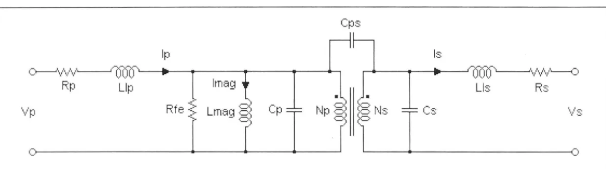
2.3 Transformer magnetics, detailed model
An "ideal" transformer transfers electrical energy from one wire to another by means of a 1nagnetic field which encircles both. In operation, one wire - the primary winding
-supplies energy to the magnetic field, while one or more other wires - the secondary windings - remove energy from it. Energy removal may be concurrent, subsequent, or both, depending on the 1node of operation. Ideal transformers are lossless, have infinite inductance, handle DC with ease, and do not exist. However, if they did exist, they would demonstrate the familiar transformer relationship:
Np/Ns = V p/Vs = I/ Ip,
where Np and Ns are the number of primary and secondary tu111s. Real transformers
routinely come within a few percent of achieving this relationship.
The following "imperfections" distinguish real transformers from their ideal counterparts:
* Winding resistance - The DC resistance of each transformer winding is usually modelled as a single resistor in series with a resistanceless winding. Its I2R heating results in what is called "copper" loss.
[2-4]
* Eddy current loss - The I2R loss associated with circulating currents induced in an electrically conductive core. These circulating currents are, in effect, resistively loaded
single tu111 secondary windings, and can be represented as a single resistance referred to ( and in parallel with) the primary.
the primary. The combined effects of eddy current and hysteresis losses are tenned core
or "iron" loss.
* Inter-winding capacitance - The distributed capacitance which exists between all the
windings of a transformer. They are usually treated as single capacitors linking one
tenninal of each winding with one terminal of every other winding.
* Intra-winding capacitance - The distributed capacitance which exists between each
tum of a winding and all the other turns on the same winding. It is usually modelled as a
single capacitor in parallel with the winding.
* Magnetising inductance - The self inductance of that portion of the primary winding
which is 1nagnetically coupled (flux linked) with other windings. It is usual to represent
this as a separate inductor in parallel with the primary winding of an ideal transformer.
Total pri1nary inductance is the sum of magnetising inductance and primary leakage
inductance.
* Magnetising current - Current which flows in the primary magnetising inductance as
the ti1ne integral of applied voltage. It is not related to any load component of primary
current (transferred from a secondary) which may also be present. It is responsible for
iron loss and contributes marginally to copper loss, but is essential for transformer
operation.
* Leakage inductance - A distributed inductance which is not magnetically coupled
with any other winding, as measured at the terminals of the winding. It is usually
considered as a single inductor in series with each winding.
* Core saturation - The condition that exists in a ferro1nagnetic material when all
do1nains have become aligned with the applied magnetomotive force (ampere turns),
resulting in a permeability approaching that of free space. A saturated core effectively
Taken together, these attributes suggest a model for the real, single secondary
transformer as shown in figure 2.3. (See also: Duffin [3], pp. 261-268; Flanagan [4]; and
Section 5.2.) The following notation is used:
Rp, Rs Primary and secondary winding resistance
Rre Resistor representing the co1nbined effects of eddy current and hysteresis loss
Cp, Cs Primary and secondary intra-winding capacitance
Cps Primary to secondary inter-winding capacitance
Lmag Magnetising inductance
Imag Magnetising current
Ip, Is Primary and secondary current
L1p, Lis Primary and secondary leakage inductance
Np, N s Primary and secondary winding turns
V p, Vs Primary and secondary voltage
Cps
Ip Is
C,_____.\.'\,•\,1
~~
·1
)(50
L---;---1---.Lip lmag
________ ___. OTif~~··,/v\/·---.:::;,
Rp LI::,
•
\/p Rf P.
<:
Ltrn.iC1~
CpI
~.Jp :g:;6?
NsI
Cs \/s-·-=--1-
-g[.
·
Tr
[image:22.787.119.737.536.709.2]O> - - - -- -_ ___.· , _ _ _ _ _ - - - - -()
Figure 2.3 Transformer equivalent circuit.
Total primary winding inductance, as seen from the input terminals (with the
secondary disconnected), is the sum of magnetising plus primary leakage inductance:
[2-5]
Any flux generated by the primary which does not pass through all turns of the
secondary contributes to primary leakage inductance. The coupling coefficient, k,
L1p = ( 1-k)Lp. [2-6]
By the same reasoning, any secondary turns which are not linked by primary flux
contribute to secondary leakage inductance,
Lis = (1-k)Ls, [2-7]
where Ls is the total secondary inductance as measured at its terminals (with the primary
disconnected).
Many magnetics texts model the transformer as a "T" network composed of three
inductors (Duffin [3], Hayt and Kermnerly [8]). In this model, the vertical leg is called
mutual inductance, M, where M = kV(LpLs). While mathematically expedient, this
n1odel has proble1ns: M does not physically exist. Also, the inductances in the
horizontal legs can assume negative values (a physical impossibility) to accommodate
turns ratios other than unity. The model is mentioned here for completeness, but will not
be used.
Switch 1node power supplies generally employ ferrite cores because they can operate
at 1nuch higher frequencies than steel or nickel alloys. Higher frequencies permit
smaller, cheaper cores because flux density is inversely proportional to both frequency
and core cross sectional area. For square wave drive,
[2-8]
where Bmax is the maximum flux density, emax is the primary voltage, f is the drive
frequency, and A111 is the magnetic cross sectional area. Therefore, for a given flux
density, increased frequency permits a reduction in core cross section. Because
transformer families have scaled standard shapes with fixed relative dimensions, this
But reduced size also implies a proportional increase in winding resistance, so
primary turns must be reduced as the square root of the linear dimension ( e.g. halving
the size implies l/"'12 turns) if copper loss is not to increase. Core loss is proportional to
frequency, core volume, and flux density:
[2- 9]
where P fe is the core loss and 1111 is the magnetic path length. Therefore, for a given
primary voltage, core loss is proportional to lrn/Np. If Np is proportional to "'1lm, then Pfe
is also proportional to "'11111 • Clearly, a net reduction in core size is possible.
However, with both Np and A111 decreasing, f must increase (as 1111
-2
·5) to maintain a
given flux density and prevent the core from being driven into saturation. The
bandwidth of the core material therefore becomes a limiting factor in size reduction.
Power ferrites are available with bandwidths up to about 1 MHz, permitting the use of
drive frequencies as high as 100 kHz. Above this speed, reduced µ and Bmax present
additional trade-offs.
Skin effect (see Billings[ 1]) has been ignored in the preceding discussion. If the
current penetration depth is greater than the conductor radius, skin effect will be
minimal. However, when the conductor is large and/or the frequency is high, skin effect
can reduce the effective conduction cross section, thereby causing resistance to increase.
Although wire diameter will tend to decrease with a reduction in core size (as 1111
°
·
75), the
frequency required to prevent saturation will increase at a much greater rate. At some
point, skin effect will begin to increase the copper loss and become an additional factor
limiting transformer size reduction.
Skin effect is significant in the primary winding and input conductors of the L VPC.
However, it does not contribute appreciably to losses in the secondary winding or output
2.4 Core saturation, cause and prevention
All ferromagnetic materials used in electromagnetic devices (including inductors, transformers, and n1otors) will saturate if flux density exceeds a critical value. The transition fro1n the unsaturated to saturated states ranges from gradual to abrupt, depending upon the n1aterial. In power ferrites and steel alloys intended for power
applications, the transition tends to be smooth but fairly rapid, with full saturation being approached gradually beyond a pronounced knee in the graph of flux density (B) vs. field intensity (H). Above the knee, increases in magnetomotive force will produce small corresponding increases in field strength, ultimately approaching those which would result if the core was replaced by air. At this point, the core becomes
magnetically useless.
The magnetising current in an inductor (including transformer and motor windings) is proportional to the applied voltage and time. That is,
[2-1 OJ
where Lis the inductance, v(t) is the voltage waveform, and iL(O) is the initial current. Flux density, B, is proportional to magnetising current ( and several other physical parameters), so it will increase with the product of voltage and time. Flux density will reach the saturation li1nit whenever the corresponding volt-second product is exceeded. This can occur if an applied AC voltage is too high, or its frequency too low, resulting in excessive area under successive positive and negative half-cycles of the waveform. It
can also occur if DC ( or an AC voltage with DC offset) is applied for too long.
the volt-time product alone. The resulting current spike increases copper loss and adds
to the voltage drop across commutation devices, both of which contribute to a reduction
in secondary voltage.
There is also a rough correlation between core permeability and coupling coefficient.
As permeability falls, less flux is confined to the core, so primary to secondary flux
linkage is reduced. For the same reason, primary and secondary leakage inductances
(and their associated voltage drops) tend to increase (Krein [9], pp. 422 and 431). This
effect also acts to reduce the secondary output voltage.
"Staircase" saturation in transformers is a gradual drift towards core saturation
resulting fro1n unequal positive or negative ampere seconds in the magnetising current.
It is usually caused by unequal push-pull primary drive, but can also result from
differing positive or negative ampere seconds in any component of secondary current
not reflected back (magnetically coupled) to the primary supply. Differing positive and
negative conduction intervals, unequal turns in split-primary windings, mismatched
rectifier diode forward drops, and variations in winding resistance can all contribute to
the problem. As one or more of these conditions exists in every real transformer circuit
employing switched primary drive, the effect is always present to some degree. It can be
a 1najor design problem. Traditional solutions include (Billings [ 1 ]):
* Inclusion of an air gap in the magnetic path to increase the ability of the core to handle
a DC flux component.
* Addition of series resistance in the primary drive circuit to decrease the applied volt
seconds at the onset of core saturation.
* Inclusion of a capacitor in series with the drive circuit to eliminate any DC component
in the pri1nary.
* Active feedback derived from primary current or voltage sensors may be used to
None of these solutions are completely effective; all involve significant drawbacks.
It should be possible to i1nprove upon the active feedback technique by continuously measuring core flux with a Hall Effect sensor located in the 1nagnetic path. Such
transducers have the advantage of being able to detect DC flux, and knowledge of this
would permit continuous adjustment of the primary drive so as to actively prevent a DC
flux i1nbalance.
Another ( and potentially simpler) alternative would be to introduce a brief mid-cycle
interruption to primary drive at the no1ninal core flux zero-crossing to enable any flux
imbalance to dissipate into primary or secondary circuitry through flyback action. With
push-pull primary drive there exists a point (nominally half way through each drive
pulse) when core flux should be zero. However, any inequality in pri1nary or secondary
ainpere seconds will shift this zero crossing in time. After many cycles, core saturation
results (unless some limiting process intervenes). If the drive transistor is momentarily
switched off 1nid-cycle (at or near the flux zero crossing), any magnetic field present
will collapse, generating a current into the supply or load circuitry presenting the lowest
i1npedance. This discharge of magnetic energy will always act in the direction required
to re-zero the core flux excursion. The process repeats twice each drive cycle.
This last technique was i1nple1nented in the initial design of the Low Voltage Power
Conve1ier (see Section 3.7), but was subsequently abandoned due to complications
relating to the presence of high levels of leakage inductance.
The flux zero-crossing flyback antisaturation technique described above is believed
to be new. No reference to it has been seen in any of the literature consulted to date.
Although not yet evaluated in a transfonner drive circuit where the additional switch-off
interval could be· tolerated, this novel concept should be of substantial benefit to
designers of drive circuits for magnetic co1nponents where staircase saturation is a
problem. The only limitation to its successful implementation appears to be related to
leakage inductance. The time required to reverse the load component of primary current
in the leakage inductance depends upon the ratio of the product of that current and
3 L VPC Design
3.1 Introduction
In 1nost designs, the DC-DC conversion process involves three basic steps. The first is co1n1nutation; the DC input must be converted to AC. Next, the AC is transformed to AC at a different voltage level, with or without galvanic isolation. Finally, the
transformed AC is rectified and filtered to produce the desired DC output. As discussed
in Section 2.2, the two principal types of AC transformation are flyback and forward. A forward conversion design was chosen for the low voltage power converter because it
offers the best possible efficiency in high power applications.
3.2 The push-pull converter
Forward converters fall into three main sub-types: Full ( or "H") bridge, half bridge, and push-pull. The full bridge type utilises four switching devices for commutation, the half b1idge uses two switching devices plus a series capacitor, and the push-pull uses two switches and a split ( centre tapped) primary transformer winding. (Krein [9], pp. 146-148.) The terminology is often blurred, with the two bridge types sometimes being given the push-pull designation also. (Push-pull refers to transformer drive in which primary current is actively driven in alternate directions, which is the case with all three types described here.) Figure 3 .1 illustrates the basic structure of the full and half bridge
designs. The push-pull forward converter is shown on the right hand side of figure 2.2.
Ln
ru
•b
x5
• 5
9 5 5
Q=i
~
as
5n__J
x5-= \•'OUT
o
oo~+
-<.
__ t
+ \l1n
Lfl
[image:29.785.148.709.826.957.2]FULL BRIDGE CONVERTER HALF BRIDGE CONVERTER
For applications involving low input voltages, commutation losses assume critical
i1nportance. In the full bridge design, input current must pass through two switching
devices in series with the primary. Both switches incur a voltage loss. While presenting
only one series switch, the half bridge design adds a series capacitor which also inserts a
voltage loss. In this application, such a capacitor would need to possess hu1norous
specifications ( e.g. C = 1 OF, ESR = 20µ0) to keep its associated voltage drop
comparable to that across the switch. The push-pull design uses only one switch in
series with each half primary. The trade-off is less a than optimal utilisation of primary
core window area. However, in this case the transformer cost is about one tenth that of
the switching transistors, so a slight increase in core dimensions is a relatively small
price to pay in relation to the cost of halving the combined switch resistance.
The push-pull split primary forward DC-DC converter topology appears to offer the
1nost promise in low voltage, high power applications. With some modification, it forms
the basis of the design implemented.
3.3 MOSFET drive circuit and snubber
The following circuit descriptions refer to the Low Voltage Power Converter
sche1natic diagram which appears at the end of this section. A List of Materials for the
L VPC is given in Appendix I.
The first step in the conversion process is commutation. Given a target output power
of 200W, an assumed converter efficiency of 80% at full power, and a 0.55V input from
a parallel solar cell an·ay, an input current of 455A is to be anticipated. If this is to be
switched with less than 10% of the input voltage lost across the switching devices, their
co1nbined "on" resistance must be less than 120µ0. An extensive search of available
switching devices revealed that the Philips PHP130N03T MOSFET yielded the lowest
resistance x dollar product available at that time (27 m0$ in 1999). With an Rcts( on) of
5m0 (typical), 42 transistors in parallel should suffice. A contact resistance of lmO per
transistor was then assumed, leading to the conclusion that 50 MOSFETs would be
It was later considered prudent to install the transistors so as to facilitate
replacement. Individual gold plated pin sockets were used, which increased the average contact resistance to about 5m0 per transistor. This resulted in a total Rcts( on) plus
Rcontact of about 200µ0 per bank. However, the copper bus bar source/drain assembly had already been machined, so the number of MOSFETs per bank remained at 50.
With O > Ycts > 1 V, PHP130N03T MOSFETs have a typical input capacitance (Ciss) of 5500pF. Of this, about 2000pF is reverse transfer capacitance (Crss), and 3500pF is gate-source capacitance (Cgs). Gate-source threshold voltage (Vth) is about 3V, but a Ygs of 1 OV is needed to ensure minimum Rcts( on). Because in this application the voltage to be switched is so small, the Miller charge is only Crss x ~ V ds = 2nC per FET. However,
the gate charge is Ciss x ~ V gs= 55nC, giving a total of 57nC x 50 = 2.85µC per bank. This charge 1nust be supplied by the gate drive circuit. A combined gate current of 1 OA could be expected to switch a transistor bank in 2.85µC/10A = 285ns. This seemed a reasonable target.
Tel Com TC4422 MOSFET driver ICs should be able to supply about 7 A into OV with a 12V supply, but their 1.50 typical output resistance would limit average 0-1 OV drive current to about 3. 7 A. A complementary emitter follower (Philips BDT81 and BDT82 power BJTs) was used to buffer the TC4422 outputs, thereby ensuring adequate current throughout the gate charge/discharge interval. A 0.470 series gate resistance was added to limit peak current to the transistors' Ic(max) of 20A. Gate rise and fall times of 500ns (for a 1 OV swing) were achieved in the actual circuit, indicating an
average gate drive current of2.85µC/0.5µs = 5.7A during the switching interval.
Averaged over one full cycle, gate drive current is only 2.85 µC x 4 transitions x 1 kHz
= 11.4 mA.
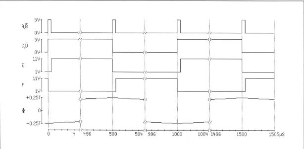
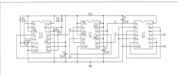
The gate drive waveforms are generated by hard-wired TTL. A 74LS123 dual
retriggerable multivibrator produces an asymmetrical 2 kHz clock with a 0.1 % duty cycle at "A" and "B" (figure 3.2). Flip-flop 2 of the 74LS74 divides this down to lkHz,
and outputs a square wave and its co1nplement at "C" and "D". Although clocked, LS74 flip-flop 1 is not used in the present drive circuit configuration. However, it is used
with the clock (and inverted clock) to produce 0.5µs break-before-make gaps in the
co1nplementary drive waveforms at "E" and "F". These gaps are necessary to prevent
simultaneous conduction in both halves of the primary, a condition which would
effectively present a short circuit to the input.
+5'·/
-R1
J
R2Z-s:-::•·)I.. ,----, . r - - 101,:::§: L..Lt, - •-...,J t',
--A1 Vee ~ -=--'•- . , . - -CR1 - \lee~ 1
_k5
~·~J
D -Ii)nF
._ ~ 1 ~Ci 10011PF ._ ~R1 LS 1....x1 11c2
.--+---+---1Q1 1·,·~· 01
C...J
-~ ) F 02
02-11r;;o~r1 ~
-11c
1 Cx2 CR2 f--1----+-___. - 01
._____,____,RC2 B2f--l----+-___. -.._G_NC_• _ _ 0__.2 -cit
1 -GND A2 - - - ,~.-.
==
~J='---+-~~~~---+-10~nF~
E,1 Bi+
-r - - \f'i Ai+
-C A2 L'· .)
\'4-I
B2 00 83-- \'2 A3 ----<
GND \'3
10nF B
[image:32.780.123.743.234.491.2] [image:32.780.125.739.686.986.2]I
Figure 3 .2 Drive waveform generator.
The drive circuit and core flux waveforms are given in figure 3.3. Note that the time
axis is discontinuous, pennitting details of the transition points to be shown.
5\/I
Jl
n
n
~
A.,B
O'v' ?/ <·<, <:~
51,.1
J
./' (.<I
co
·., O'v'11\,,'I
JJ
'. .;·.:·
.;.,
I
E1\1 >· ... .,
11 \''I
l
I
(<
I
F
11,1
<, ..
:c":ct
+025:1
:-=~ ~?
T
</----.:."/ :,.:::..._
-?
:,,
-0.25T '":'"
~· ..
' '
0 Lt Lt96 500 50Lt 896 1000 100Lt 1 Lt96 1500 1505fJ13
Magnetic energy- predominantly that component stored in transformer primary
leakage inductance - is released following each drive interval. This energy produces an
Ldi/dt voltage spike across the switching device unless it is diverted to some other
co1nponent. A snubber circuit is used in which fast recovery diodes D 1 and D2 divert
switching transients to capacitors C15 and C16, where they are temporarily stored until
being returned into the +O. 5 5V input through resistors R 7 and R8.
In this device, transformer leakage inductance referred to the primary is about 140nH
(see Section 5.2). With an input current of 155A, stored energy is V2LI2, or l.681nJ. At 1
kHz, 1000 x 1.68mJ x 2 off-transitions, or 3 .36W could be released. Each l.681nJ spike
would charge the (2 x lOµF) snubber capacitors to about 13.0V (W = V2CV2), if the
switching interval is long enough. However, -r =~(LC)= 1.67µs, so the capacitor
voltage can only rise by a 1naximum of about 3.9V during each 0.5µs t0ff interval. (It
actually rises by 5.2V, probably because charging continues beyond the t0ff interval. See
Section 6.2 for further discussion.) Most of the re1naining leakage current will continue
to circulate in the primary where it will act in opposition to the next drive pulse. Except
at very low current levels, the voltage across the snubber resistors will be greater than
the input supply voltage. Therefore, only a portion of the stored energy will be returned
to the +0.55V input. Most will be dissipated in the snubber resistors.
In the absence of a snubber circuit, switching transient power would be dissipated in
those few MOSFETs in each bank which happened to have the lowest drain to source
breakdown voltages. While repetitive drain-source breakdown is not necessarily
damaging to FETs, such operation is not recommended.
3.4 Drive circuit power supply
The following circuit descriptions refer to the Low Voltage Power Converter
schematic diagram which appears at the end of this section.
Power to operate the logic and MOSFET driver circuits is derived from an auxiliary
V AC square wave, which is rectified and filtered to produce unregulated 12 VDC for
the FET drive stage. A 78L05 linear regulator is then used to establish the 5.0 VDC rail
for the TTL waveform generator. Total power consumed by the drive circuit and its
associated power supply is about 0.6W. Drive circuit power is linearly dependent upon
L VPC input voltage, but independent of output load.
Because the auxiliary winding delivers power only after operation commences, a
start-up circuit is required. For this purpose, a small 9V battery is momentarily
connected to the 12V supply rail to enable FET drive to commence. The supply
beco1nes self-sustaining after the first few cycles, so the momentary contact battery
switch (S 1) can be released. In view of the low input voltage to the L VPC, any
automatic start-up circuit would probably need to employ either battery power or
germanium transistors (Vbe;:::::; 0.3V). However, it was not considered necessary to
incorporate an auto-start feature at this time.
An "interesting" start-up problem was observed during initial prototype testing.
When the start button was pushed, the first drive pulse would be generated as soon as
the LS 123 commenced oscillation, which occurred when the logic supply reached about
3.5V. The gate current associated with the first drive pulse would depress the raw
supply voltage (then about 5.0V) which, in tum, permitted the logic rail to fall below
3.5V. This caused the LS 123 to reset briefly until its supply again reached the minimum
operating level. The resulting power supply oscillation caused excessive drive current to
flow into the combined gate capacitance, which effectively clamped the 12V drive
circuit supply rail to 5V, thereby preventing normal start-up.
A start-up inhibit circuit was added to correct this problem. In operation, this circuit
disconnects the 5V rail until the 12V rail filter capacitor (Cl 7) has charged to at least
7.5V. Zener diode D12 sets this voltage in conjunction with RlO and Rl3. These two
resistors also provide hysteresis, which is required to prevent the start-up inhibit circuit
from oscillating. With 2.5V headroom, the linear regulator can comfortably maintain the
5V rail until normal operation of the auxiliary secondary is established (within several
event of reduced input voltage (<0.3V). It will also shut down the LVPC under severe
overload conditions.
3.5 Transformer design
In an ideal transfo1mer only the turns ratio is important. The actual number of turns
is irrelevant. This is true because primary inductance is infinite, so there is no
1nagnetising current. In a real transformer primary inductance increases, and
1nagnetising current decreases, as the square of primary turns:
[3-1]
where µ is the pe1meability of the core material. Core flux density ( and therefore core
loss) increases linearly with the volts per tum ratio (Bmax = emaxl4fNpAm) so, for a given
pri1nary voltage and frequency, increasing primary turns will cause core loss to fall
proportionately. For most core materials the area enclosed by the magnetisation curve,
and therefore core loss, tends to increase rapidly as saturation approaches. For this
reason the knee of the magnetisation curve - not the actual saturation limit - is used to
establish the maximu1n pennissible volts per tum ratio.
Unfo1tunately, primary resistance (and therefore copper loss) increases with the
square of the number of pri1nary turns. This is because, for a given core, winding length
increa es in proportion to turns while the window space available for each tum (i.e. the
wire cro sectional area) decreases. The transformer will be most efficient when the
um of copper and core losses is minimised, and this condition often occurs when these
lo e are nearly equal.
Tran former design is usually an iterative process. There are so many interdependent
et different! weighted variables that an optimal design based on their simultaneous
solution i often impractical. Therefore, the first step is to reduce the number of
Assumption 1: Each half of the split primary winding will consist of a single tum.
This assumption is dictated by the fact that any primary designed to carry 450A is
going to have a large cross section, and will very likely have to be machined from solid
copper. Also, while fractional turns ( e.g. 2.5) are technically possible (with an EI or EE
core), they are significantly longer than their closest integral counterparts because turns
are applied to the outside legs. They will therefore present significantly more resistance.
Assumption 2: A standard, off-the-shelf EE core in power ferrite will be used.
As the L VPC is a switch-mode power supply, it was assumed the general rule that
"faster is better" would apply (see below), and that power ferrite was therefore an
appropriate choice for the core material. This assumption later proved to be partly
incorrect, but because the prototype design was based upon a ferrite core, this will be
considered first.
For a given power level, larger cores tend to be more efficient than smaller ones.
This is because windings can be thicker and flux levels lower, so both copper and core
losses reduce as size increases. Of course, larger cores are more expensive. But in this
design the cost of the largest readily available core set and winding bobbin (about
$15.00) was negligible compared with the cost of MOSFETS ($547.00) and other
components. An E65/32/27 core set was selected. Samples were ordered in Philips 3C90
and N eosid F5 1naterials, both of which have similar specifications.
Assumption 3: A nominal output of 25VDC at 8ADC (200W) is appropriate.
Choice of output voltage is relatively unimportant. The intent of the design is to
establish the practicality of constructing an efficient DC-DC converter for use at very
low input voltages. Except at very high voltages (where thick insulation displaces
copper cross section in the window), transformer efficiency is almost independent of
voltage. 25V is a good compromise between electrical safety and convenience, and
many DC/ AC inverters operate with this voltage as a nomi~al input. Also, fixed losses
associated with rectifier diode forward drops are less significant at 25VDC than they
With these three assumptions made, transformer design is straightforward. It should
be noted that magnetics calculations may be carried out in either the mks system, in
which B, H and <D carry the units Tesla, Ampere turns/metre and Weber, or in the cgs system, where the same parameters are measured in Gauss, Oersteds and Maxwells. The mks system is gradually displacing cgs in the literature, and will be used here (with the
exception of s1nall linear dimensions, where metres can be cumbersome). In the
discussion which follows, reference will be made to the core's mechanical and magnetic parameters as set forth below.
E65/27 /32 core set design parameters:
Magnetic path length (effective) le 14.7 cm
Magnetic cross section (effective) Ae 5.35 cm 2 Permeability (effective) µe 2.0mH/m Bobbin winding window area Aw 3.92 cm 2
Length of tum (mean) lT 15.1 cm
Because primary and secondary windings carry equal ampere turns, core losses are
usually 1ninimised by assigning half the winding window area to the primary, and half to all the secondaries. (This is not strictly true when a split primary is combined with an
un-split secondary, but the difference is negligible. The proof is tedious and
uninformative.) The coil former (bobbin) window comprises two sections separated by a partition, each 1neasuring 1.92 cm wide by 1.0 cm deep. Allowing for 0.06 cm
insulation (air and epoxy) between them, both split primary turns should be able to have rectangular cross sections of 0.93 x 1.0 cm, and a length of 15.1 cm. Each half-primary willhavea DCresistanceofplT/A=(l.73 x 10-6)(15.1)/(0.93)=28.1 µO. Skin effect (see Section 5 .1) will cause the effective resistance to be somewhat higher, but it still compares favourably with the as-designed switch resistance of 120µ0.
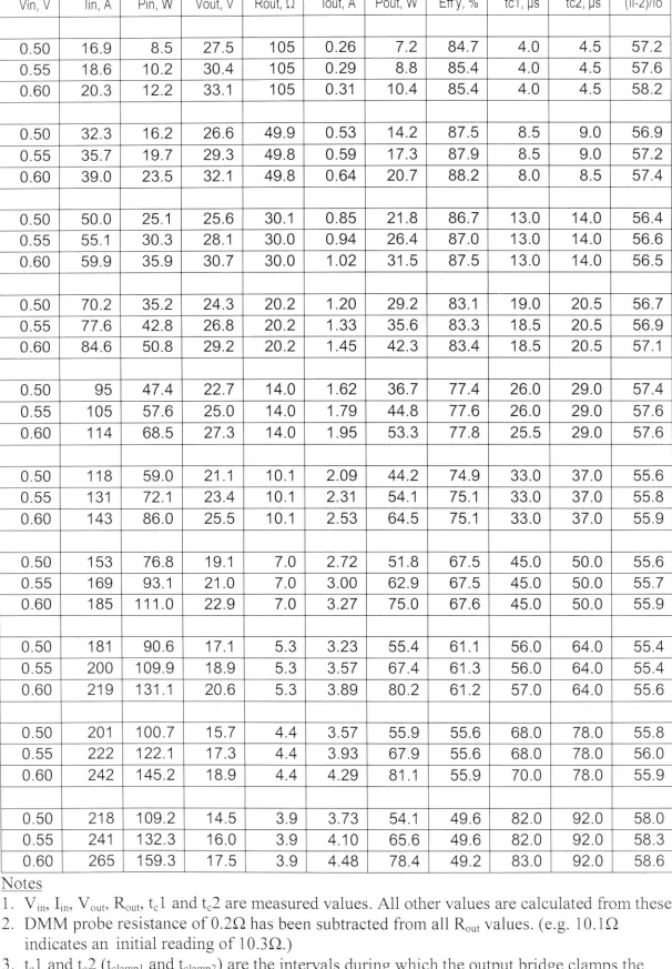
If the LVPC is to operate with a nominal input of 0.55 VDC, and if 455A x 120µ0 =
MBR6045 Schottky diode bridge rectifier (Vf = 0.50 x 2 at Ir= 8A) plus its own
winding resistance, and still supply a nominal 25VDC at full load.
Primary lpRp drop is about 2.6% of the applied voltage. If it is assumed that the
secondary will experience the same percentage voltage drop as the primary ( a
reasonable first-pass approximation), then about (25.00 + 1.00) x 2.6% = 0.68 V will be
lost. Therefore, the secondary should have sufficient turns to produce 26.68V, or Ns =
26.68/0.482 = 55.4 turns. As fractional turns are impractical, Ns should be 56 turns.
The window area available for the secondary also measures 1.92 x 1.00 cm. To
achieve maximum fill factor, layer winding should be employed. Consideration of the
available dimensions leads to the conclusion that 6 x 11 tum layers results in the largest
possible wire diameter consistent with the requirement for 56 turns. The resulting
optimum wire diameter is 1.66 mm; the closest standard wire size is 1.5 mm. Even with
1.5 mm wire, insulation thickness, layering imperfections, and the fact that the last tum
on each layer is also the first tum on the next combine to limit the actual number of
turns per layer achievable in practice to 10. Although the design called for 56 turns, 58
turns were actually applied because space was available. This was done under the
assumption that removing unwanted turns would be much easier then adding them later
if modification proved necessary.
The secondary will have a DC resistance of plTN/ A=
(1. 73 x 10-6)(15 .1)(58)/(0.0177) = 85 .6m0. Skin effect should not be significant with
wire of this diameter. Note that 8A x 85.6mQ = 0.68V, or about 2.4°/o of the nominal
full load secondary voltage of 0.482 x 58 = 27.96V. The assumption concerning voltage
drops of similar percentages in the primary and secondary was justified. The fill factor
is (0.0177 x 58)/1 .92 = 53.5%, which is normal for layer winding.
Con erter performance can be estimated by substituting values for Rp, Np, s, and Rs
into the transformer model given in Section 2.3. AC parameters and core loss may be
ignored at this stage. Considering only DC losses, (Vin - IpR:is - IµRcontact - IpRp)(Ns/Np)
If Vin = 0.55V, Rcts(on) = 100µ0, Rcontact = 20µ0 (the pre-socket value), and Rp, Ns,
Np, Vf and Rs are as stated above, then Yout = 30.9 - 0.5838Is. For Pout= Youtls = 200W, Yout = 26.49V and Is= lout= 7.55A.
tn
=Ip= 58Is = 437.9A, so Pin= 240.8W. Therefore conve1ier efficiency, ri = 83 .0%. Transformer copper losses will be Ip 2Rp+
I/ Rs =5.39W + 4.88W, or about 5% of output power, giving a transformer efficiency ( discounting core losses) of about 95°/o.
As mentioned above, the addition of MOSFET sockets caused Rcontact to increase to 100µ0. The result of this change is that Yout = 23.70V, lout= 8.44A, and ll = 74.3% if a 200W output is to be maintained. A more accurate AC evaluation using the full circuit model will give somewhat more pessimistic results (see Section 6.2), however the turns ratio and copper loss appear to be satisfactory.
Operating frequency must be determined by evaluating conflicting trade-offs. Higher frequencies involve higher switching losses. Because a fixed interval is required to
reverse current in the leakage inductance, higher frequencies also reduce the effective d1ive duty cycle, thereby increasing RMS current ( and copper losses) in the windings. Core loss is proportional to both drive frequency and Bmax, but as Bmax is proportional to 1/f, drive frequency does not significantly affect core loss unless Bmax is pushed beyond the knee of the magnetisation curve. For the ferrites considered here, the magnetisation curve begins to bend noticeably at about 350mT, and inputs up to 0.67V are possible (see Section 2.1). With Bmax = emaxl4fNpAe = 0.67/4f(5.35 x 10-4), £nin = 895Hz.
A preconception that a good starting point for ferrite core drive is a frequency just above the audible range gave 25kHz as the initial selection. However, dismal
preli1ninary test results quickly led to this being reduced, first to 2.5kHz, and then to 1.0kHz. Incipient core saturation due to drive pulse imbalance or unequal primary coupling has fixed 1.0kHz as the lower practical limit with this core (see Section 5.3). At this frequency, and with VP = 0.50V, Bmax is nominally 234mT.
core loss proportional to drive frequency and flux density, at lkHz and 234mT it should
be about 426mW for 3C90 and 683mW forN27/F5. Therefore, if VP= 0.5V, then Rfe
will be 587m0 and 366m0 for the two materials, or 477m0 average. However, at about
0.3o/o of maximum output power, core loss is nearly 20 times less than copper loss, and
therefore practically insignificant.
Transfonner pri1nary magnetising inductance, Lmag = µeN/ Aefle, or 7.28µH for the
transformer as wound. Measurements made on the N eosid core using a Marconi
TF1313A impedance bridge confirmed primary inductance as 7.3µH (Q = 0.80) at lkHz
and 7.2µH (Q = 0.70) at lOkHz. Secondary inductance measured 28.SmH (Q = 34) at lkHz, which is reasonably close to the expected 582Lµ. Core bandwidth was measured
with Np= Ns = 9, Vµ = 2.50Vpeak (sinusoid), Rsource = 330, and R1oa<l = 1000. Under
these conditions
fc
= 1.2MHz, where Vs = 2.51"'12 V peak at an angle of -50°. Vs rolled offsmoothly with increasing frequency.
3.6 Leakage inductance minimisation
As stated previously, transfonner leakage inductance is a distributed inductance in a
winding which is not magnetically coupled with any other winding. Although not part
of the transfonner, any uncoupled inductance in series with a transformer winding adds
to the effective leakage inductance. For this reason, inductance associated with the
wiring to and from a transformer should also be minimised.
Leakage inductance is a problem for several reasons. First, the L1di/dt voltage
developed across it always acts to oppose the voltage applied to or developed by a winding, thereby reducing the effective turns ratio. Also, a finite amount of time is required twice per cycle for load current to reverse in the leakage inductance. To
maintain the same average current, the RMS current must increase as the reciprocal of
Because of the high di/dt's associated with switching large currents, the LVPC is particularly vulnerable to the adverse effects of leakage inductance. This fact was only
vaguely appreciated during the early design stages, but it has become by far the most
troublesome obstacle to attaining the desired performance.
Current is supplied to each half-primary through copper bars machined fro1n the
saine piece of copper as the winding itself. These bars are parallel and closely spaced,
so that flux generated by each will partially link with and, because the currents are equal and opposite, partially cancel the flux from the other. One bar carries input current from the positive supply to the transformer. The other connects to the drains of the 50
MOSFETs which drive the associated half-primary. The sources of these MOSFETs connect to a third copper bar which parallels the others and forms the negative return for the circuit. The length of the bars is about 270mm, corresponding to fifty T0-220
transistor packages 1nounted at 5mm spacing.
The L VPC draws discontinuous current, primarily because of the dip produced during the time required to reverse load current in the leakage inductance. Under these conditions, cable inductance produces undesirable Ldi/dt voltage spikes at the L VPC input, despite its being filtered by 3 x 4.7mF low ESR capacitors. For this reason, it was
also necessary to reduce the inductance associated with the cables supplying current to
the conve1ier. Parallel cabling was impractical, so shortening the battery/regulator/
L VPC loop to around 850mm was the best that could be achieved.
3. 7 Antisaturation feature
The LVPC design initially incorporated a feature intended to prevent core saturation
(see Section 2.4). With the fundamental drive frequency set at 2.5kHz, the MOSFETs
were switched off midway through each 195µs on-interval to permit any flux imbalance
to dissipate into primary and/or secondary circuitry through flyback action. This was
achieved by running the 74LS 123 multivibrator at 10 kHz, with a 4.5% duty cycle at