1
PV Single Phase Grid Connected Converter: DC-link Voltage Sensorless Prospective
N.E. Zakzouk, A.K. Abdelsalam, A.A. Helal
B.W. Williams
Electrical and Control Engineering Department Electronics and Electrical Engineering Department Arab Academy for Science and Technology (AAST) StrathclydeUniversity
Alexandria, Egypt Glasgow, United Kingdom
Abstract--In this paper, a DC-link voltage sensorless control technique is proposed for single-phase two-stage grid-coupled photovoltaic (PV) converters. Matching conventional control techniques, the proposed scheme assigns the function of PV
maximum power point tracking (MPPT) to the chopper stage. However, in the inverter stage, conventional techniques employ
two control loops; outer DC-link voltage and inner grid current control loops. Diversely, the proposed technique employs only
current control loop and mitigates the voltage control loop thus eliminating the DC-link high-voltage sensor. Hence, system
cost and footprint are reduced and control complexity is minimized. Furthermore, removal of the DC-link voltage loop
proportional-integral (PI) controller enhances system stability and improves its dynamic response during sudden
environmental changes. System simulation is carried out and an experimental rig is implemented to validate the proposed
technique effectiveness. In addition, the proposed technique is compared to the conventional one under varying irradiance
conditions at different DC-link voltage levels, illustrating the enhanced capabilities of the proposed technique.
Keywords—Photovoltaic; MPPT; grid connection; DC-link voltage control; Single Phase Converter
I.
Introduction
Currently, renewable energy resources are supplying significant share of global energy generation due to the increasing costs and
decreasing reserves of fossil-fuels, as well as their environmental problems. Among the former, photovoltaic (PV) energy has gained
much interest as a less pollutant and noise-free resource that has the capability to be expanded and utilized in rural areas [1-2].
Common distributed energy resources (DERs) are increasingly being connected to utility for best utilization of their produced
electric power [3-7]. A number of grid interfacing methods have been proposed for PV-grid connection [8, 9], among which string
inverter topology is widely used at present. It overcomes the drawbacks of old centralized inverter topology where multiple PV strings
are connected to a central inverter, thus suffering from non-flexibility and power losses due to maximum power point tracking (MPPT)
mismatch. Alternatively, for string inverter method, a number of PV modules are connected in a series arrangement called a string and
each has its own inverter [10] and the system can be expanded by additional strings with their associated inverters [11, 12].
For successful interface of PV strings with the grid, a number of requirements arise [13, 14]. First, maximum power point tracking
(MPPT) of the PV string is mandatory to maximize system efficiency as the performance of a PV source relies on the operating
irradiance and temperature conditions [15]. Furthermore, voltage regulation at the inverter DC-link and grid current control are
2
inverter stage which achieves PV MPPT and PV-grid interface functions. Hence, component count is minimized; increasing
conversion efficiency [16, 17]. A major drawback of this topology is voltage ripples on the DC bus resulting from double
line-frequency grid power oscillations due to single-phase connection [18]. Hence, for a single-stage topology, the inverter must be
designed to handle these ripples using large electrolytic capacitors to limit the ripples' propagation to the PV output power [19]. These
capacitors are a limiting factor of the inverter lifetime and reliability. Two-stage topology is presented, as another alternative, where a
power decoupling DC-DC stage is added before the inverter stage, at the cost of additional components and losses [20, 21]. However,
this additional stage decouples the energy change between the PV string and the DC-link capacitor of the output inverter stage.
Furthermore, this additional stage can boost the PV voltage level thus expanding its operating range and increasing flexibility for the
number of PV modules used [8].
Conventionally, the first DC-DC chopper stage achieves MPPT while the second inverter stage delivers energy to the grid [22-25].
PV string inverter features: outer DC-link voltage control loop and inner grid current control loop. The former regulates the DC-link
voltage and adjusts the reference grid current to guarantee power flow to grid and satisfy power balance at DC-link, while the latter
forces the inverter to produce near-unity power factor sinusoidal line current.
Hence, for conventional control strategy, measurements of PV voltage and current are required to achieve MPPT. Furthermore,
sensing DC-bus voltage is mandatory for the outer DC-link voltage control loop and measuring grid voltage and current is essential for
the inner grid current control loop. Sensorless control techniques have been proposed for this configuration to reduce these
measurements and in-turn lessen the required sensors, simplifying system structure and reducing size and cost. However, most
researches involve elimination of PV voltage and/or current sensors [26-31]. These techniques are based on sensorless MPPT control
scheme fact that as the DC-link voltage is kept constant by the controller action at steady-state, PV generated power and grid side
power should be in balance [32-33]. This will force the grid current’s amplitude to be proportional to the PV generated power. Thus,
varying the chopper duty cycle to maximize the line current amplitude will result in PV MPPT without the need of PV sensors.
However, overall system response deteriorates in comparison with that of the conventional method which directly detects PV power.
This can be related to the fact that the response of this sensorless MPPT operation directly depends on the response of the inverter
DC-link voltage control loop and consequently its grid current control loop [34].
In this paper, a DC-link voltage sensorless technique is proposed based on the fact that if the PV maximum power is forced to flow to
the grid, then power balance at the inverter DC-link will be satisfied and DC-link voltage will stabilize by nature without the need of
outer DC-link voltage control loop. Hence, the proposed scheme still requires PV sensors to directly calculate the PV power, but
eliminates the high cost DC-link voltage sensor, thus reducing system footprint and cost. Furthermore, the removal of the DC-link
3
irradiance changes. Simulation and experimental results verify the proposed scheme effectiveness at different DC-link voltage levels
and confirm its superior performance over that of the conventional scheme under varying irradiance conditions.
II.
System Under Investigation
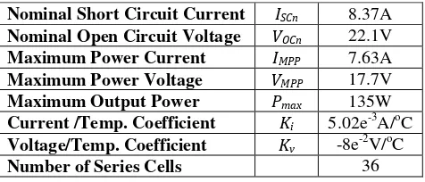
The considered system is a 1.5 kW, 220 V, 50 Hz single-phase two-stage grid-connected PV system as shown in fig. 1 (a). The first
stage is a boost converter responsible for MPPT process, voltage amplification, and decoupling between the PV source and the
DC-link. The second stage features a current-controlled voltage source inverter (VSI) for grid interface. The PV source, in this paper, is a
string configuration which consists of ten KD135SX_UPU PV modules connected in series. The PV array specifications, in addition to
the system design, are listed in Appendix 1 TABLE I;
(a) (b)
[image:3.612.47.547.252.461.2](c) (d)
Fig.1: PV-grid connected system under investigation (a) system configuration, (b) power balance at inverter link, (c) Mean DC-link voltage, and (d) Average active grid power.
III. Power Balance at DC-Link
Equation(1) represents the power balance at the inverter DC link [19, 22, 23, 41and 42], as illustrated in fig. 1 (b). = + (1)
where Pdc is DC-link input power, pinv is instantaneous power supplied to inverter, and pcap is instantaneous DC capacitor power.
= (2)
where vdc is the instantaneous DC-link voltage.
Assuming the AC line current (ig) is sinusoidal and in-phase with the AC grid voltage (vg), equation (3) results:
4
where is the instantaneous active powerinjected to the grid assuming unity power factor, is the grid voltage, is the injected
grid current, and is the average active power injected into the grid.
Thus, by substituting (2) and (3) in (1), equation (4) results:
= (1 − cos(2)) + (4)
From (4), it is clear that there are two power components inside the DC-link capacitor. The first is the average power difference
between Pdcand Pg, which is a DC component that causes a linear increment or decrement in the DC- link voltage. The second one is
the grid power ripple of twice the AC mains frequency, which results in a double line-frequency ripple in the DC-link voltage. The
DC-bus capacitor should buffer this power differences as well as minimize the voltage ripple [19]. In order to achieve the latter, energy
is acquired by the DC capacitor. Energy balance equation can be obtained by integrating (4) over one cycle:
$= $+12 (5)
where Edc is the input energy to the DC-link, Eg is the energy captured by grid and &= $ which is the energy stored in
DC-link capacitor.
As shown in in fig. 1 parts (c) and (d); for the same DC power, as DC-link voltage level increases, the power transferred to the grid
is reduced.
This is mainly related to the fact that besides the energy acquired by the DC capacitor, there are other parameters that increase grid
losses and are DC-link voltage dependent as well. These are converter power losses (pconv-loss) which include switching and
semiconductor losses, in addition to losses in DC capacitor equivalent series resistance [43].
Equation (4) doesn't take these losses into account although this would introduce a disturbance into the power balance equation
that results in a steady-state error in the DC-link voltage. Thus, they must be taken into account [41] as follows:
= (1 − cos(2)) + + '()'** (6)
In order to satisfy the power balance equation at the inverter DC-link, the DC-link voltage should be kept constant at a
certain predetermined level. This will ascertain the PV power is transferred to the grid which guarantees power flow from the
5
IV. Control Techniques for Grid–connected PV Converters
PV-grid interface is commonly achieved using conventional DC-link voltage sensored control technique [22-25]. However,
in this paper, a DC-link voltage sensorless technique is proposed to realize this interface. Control schemes of both techniques
are modelled, analysed and their performance is compared to validate the proposed scheme feasibility.
A. Conventional Control Technique
The conventional control scheme is shown in fig. 2(a). Boost chopper switching is directly controlled using the appropriate
duty ratio produced by the MPPT algorithm.
Various MPPT techniques are presented in literature [44, 45] among which variable-step incremental conductance
(IncCond.) technique is of special interest due to its simplicity, high accuracy and less computational burden [46-48]. For better
performance and simpler implementation, the modified variable step-size IncCond. technique, presented in [49], is applied.
On the other hand, DC-link voltage regulation as well as grid coupling are achieved using current controlled VSI that inhibits
two control loops; the outer DC-link voltage control loop, fig. 2(b), and the inner grid current control loop, fig. 2(c).
1. Inner grid current control loop
The inverter is required to output a sinusoidal grid current with acceptable THD and near-unity power factor. Thus, the
output of the DC voltage controller, which represents the reference grid current amplitude, is multiplied by a sinusoidal unit
vector which is obtained from a phase-locked loop (PLL) synchronized with the grid voltage. Then, the inner current loop
controller forces the grid current to match this sinusoidal reference. The block diagram of the inner grid current control loop is
shown in fig. 2(b).
The most common types of controllers used for the inner current loop are; proportional-integral (PI) with feed-forward and
proportional-resonant (PR) controllers [50-54]. However, PR controllers' performance outweighs that of the traditional PI ones,
when regulating sinusoidal signals [13]. The former have the ability to remove the current's magnitude and phase angle
steady-state errors without the need of voltage feed forward unlike traditional PI controllers. Thus, an ideal PR controller is applied for
the inner grid current control loopwith a gaingiven as [52-54];
,-.() = /-(0+ /1(0+ (7)
where /-(0 is proportional part gain, /1(0 is the resonant part gain and ω is the resonant frequency of the controller. The
desired sinusoidal signal’s frequency is chosen as the resonance frequency, which is the grid line angular frequency in this case.
The PR controller gains are designed achieving high gain (almost 50 dB) at a bandwidth around the resonant frequency (about
6
variations. However, it should be remarked that if severe grid frequency variations are registered in the utility network; a
modified PR controller is necessary [55, 56] or a non-ideal PR controller can be used to give a wider bandwidth around the
resonant frequency [57, 58]
The converter operates at high switching frequency, so the PWM block can be represented by a simple gain [23, 24]
/-34 =5* 5607
8 (8)
where :607 is the amplitude of the triangular carrier signal.
2. Outer DC-link voltage control loop
This loop is responsible for DC-link voltage regulation by adjusting 80;< which is the amplitude of the sinusoidal reference
grid current that must be in-phase with the grid voltage (vg). The current amplitude (80;< ) represents the active component of
the reference grid current which indicates the instantaneous amount of power available at the DC side of the inverter (pinv) [41].
By accurately adjusting this current amplitude and using a fast grid current controller, the power at the inverter DC side is
transferred to grid. Thus, power balance at the DC-link is achieved which makes Vdc stabilizes at the required level. However, in
order to compensate for system losses given in (12) (i.e. inverter losses and losses due to the parasitic series resistance of Cdc), a
decrease in the power available at the inverter side occurs which in-turn decreases 80;< . The latter imposes losses on the grid.
The block diagram of the outer DC-link voltage control loop is shown in fig. 2(c). The implemented voltage controller can be a
simple proportional controller [24]or a proportional-integral (PI) one [23]to minimizethe DC-link voltage steady-state error.
The latter is used and it is represented by the gain GPI(s) where /-( and /1( are proportional and integral gains of the DC-link
voltage PI controller respectively:
,-1() = /-(+/1( (9)
These gains must be precisely designed for a low cross-over frequency (10-20 Hz) in order to attenuate the magnitude of the
double line-frequency DC-link voltage ripples. Thus, oscillations in grid current reference are limited.Otherwise, grid current
THD may exceed the limit and a larger DC capacitor is required, to overcome these oscillations, which in-turn reduces the
inverter life-time. To illustarte this issue, the PI gains are first designed with initial values computed from Ziglar/-Nicholes
method followed by successive tuning aiming at achieving grid current THD within IEEE 519 Std. [59]. Hence, the outer loop
controller gains are selected as; KP-i=0.01 and KI-i=0.5 giving a cross-over frequency of almost 20Hz as shown in the bode plot
in fig. 2(e). In this case, the system shows minimal grid current THD however at the cost of slower response during changes. If
7
harmonics limits [59], as shown in fig. 2(f). The DC-link volatge in addition to the grid current controllers detailed parameters’
tuning is illustrated in details in Appendix 2.
The inner grid current control loop, with a bandwidth of a few kHz and unity feedback, can be represented by a unity gain at
the low frequency range considered for the voltage control loop [23] as shown in fig. 2(c).
The relationship between variations in the fundamental grid current magnitude and the mean DC-link voltage can be
calculated using the average power balance equation derived from differentiation of (5) by time, assuming that the converter is
lossless.
= + >12 ?
(10)
For simplified sensitivity analysis, when studying relationship and correlation between certain system variables, other
variables of least contribution and effect, on the studied variables, can be partially eliminated. Hence, for determining the impact
of the grid current magnitude variation on the average DC-link voltage, one neglects Pdc[23]. Assume zero PV power, then
Pdc=0, DC-link capacitor energy ($) is solely affected by grid power as follows;
$
= >12
?
= − (11)
>12?
= −
2 (12)
Applying small perturbations around the operating point leads to:
>12(+ (;06)?
= −ABC+ D̂2(;06F (13)
where (;06, and D̂(;06are the small perturbations applied around the mean DC-link voltage and the grid current amplitude
respectively. Neglecting steady-state values and square of small perturbations
>122(;06?
= −AD̂(;062 (14)
Hence, equations (15) and (16) can be concluded;
() = −AC2 (15)()
()
() = −
8 B. Proposed DC-link Voltage Sensorless Control Technique
In the proposed technique, MPPT is achieved, similarly as in the conventional technique, by sensing the PV voltage and
current. However, the proposed technique involves only one control loop in the second inverter stage which is the grid current
control loop, thus mitigating the inverter outer DC-link voltage control loop with its PI controller which in turn simplifies the
overall control scheme. Moreover, the high cost DC-link voltage sensor is no longer required, reducing the system footprint and
cost. The proposed control scheme is shown in fig. 3(a).
≥
(a)
(b)
(d)
(c)
(e) (f)
Fig. 2: Conventional control technique; (a) control scheme, (b) inner grid current control loop, and (c) outer DC-link voltage control loop, (d) bode plot of grid current loop PR controller, (e) bode plot of DC-link voltage loop PI controller, (f) Grid current THD at different irradiance level for 2 values of proportional gain (KP-i) applied in the DC-link voltage PI controller.
0% 5% 10% 15% 20%
400 600 800 1000
%
T
H
D
Irradiance (W/m2)
9
In the conventional technique, DC-link voltage regulation and 80;< adjustment are achieved using the DC-link voltage
controller as explained in the previous subsection. Alternatively, in the proposed method, the DC-link voltage is stabilized and 80;< is adjusted without the need of an outer DC-link voltage control loop. In the proposed control technique, the PV voltage
and current are sensed to achieve MPPT. Depending on the tracked maximum PV power value, the amplitude of the reference
grid current is adjusted. The grid current controller forces the inverter to produce a sinusoidal current with a magnitude matching
that of the reference current which corresponds to the tracked maximum PV power. Thus, the PV maximum power is forced to
flow to the inverter AC side satisfying the power balance at inverter DC-link hence forcing the DC-link voltage to stabilize by
nature at a certain level without the need of a voltage controller.
1. Without system losses compensation
The proposed control technique, when adjusting80;< , must guarantee that the tracked PV maximum power is transferred to the
grid so that power balance is achieved at inverter DC-link and Vdc stabilizes by nature without the need of DC-link voltage
controller. Hence, 80;< is determined by dividing PV maximum power at certain environmental condition (PPV) by grid voltage
rms value (Vg), as shown in (17). This amplitude is then multiplied by a sinusoidal template of the grid voltage derived from
PLL. The grid current PR controller, similar to the one employed in the convention control technique, forces the inverter to
produce a sinusoidal grid current that matches this reference. The uncompensated grid current control loop is shown in fig. 3(b).
8(JKLM) = √2 0;< -O
(17)
However, this uncompensated scheme doesn't take into account system losses which include converter power electronics
switches' losses and the losses due to the parasitic series resistance in Cdc. Thus, a disturbance in the power balance at DC-link
occurs and the DC-link voltage reaches value less than grid voltage amplitude ( ) which means that the modulation index (ma)
may reachunity, imposing harmonics in the grid current beyond acceptable limits as will be demonstrated at the end of this
subsection.
2. With system losses compensation
System losses must be taken into account to guarantee power balance at inverter link. However, due to the absence of
DC-link voltage control loop in the proposed technique, there must be an alternative way to compensate for these losses. Since these
losses decrease the active grid power, then the grid current in turn decreases. Thus, the reference grid-current amplitude must be
readjusted by a compensating component as shown in (18):
8(KLM) = √2 P0;< -O
10
where Icomp is the rms value of the compensating current (icomp). This current represents the decrease in grid current amplitude,
and in turn the decrease in grid reference active power to compensate for system losses. Thus, power balance and flow are
ensured, achieving DC-link voltage stabilization. According to Icomp value, Vdc can be kept at a level that ensures that M≤ 1
which results in acceptable grid current THD. The proposed compensated grid current control loop is shown in fig. 3(c).
≥
2
÷
(a)
2
÷
(b) (d)
(e) 2
÷
11
(f)
Fig. 3: Proposed DC-link voltage sensorless technique; (a) control scheme, (b) uncompensated grid current control loop, (c) compensated grid current control loop, (d) PPV -Icomp mapping for DC-link voltage of320V and 400V, (e) Configuration of the proposed feed-forward ANN for PPV -Icomp mapping, and (f) PPV-Icomp empirical relation determination flowchart
At certain Vdc level, as PPV increases, system losses increase which in turn requires the increase of Icomp to compensate for
these losses. Thus, for constant Vdc, Icomp depends on PPV and varies proportionally with it however in a non-linear form.
Moreover, as Vdc increases, for constant PPV, system losses increases which results in an increase in Icomp to compensate. Figure
3(d) shows the empirically obtained non-linear relation between PPV and Icomp at two different Vdc values for the investigated
system. It can be noticed that at Vdc=320V (i.e. ma≈1), Icomp has lower value which in turn decreases losses imposed on grid.
Hence, mapping between PPV and Icomp, at a predetermined Vdc level, is system-dependent and mandatory in order to achieve
the proposed DC-link voltage sensorless scheme. The PPV-Icomp mapping can be implemented using a simple look-up table.
[image:11.612.156.438.47.503.2]12
network (ANN) is proposed in this paper featuring an input layer, a hidden layer and an output layer as shown in fig. 3(e). The
input represents the PV power while the output layer generates the compensating current corresponding to the input PV power
and required to stabilize Vdc at a predetermined level. The applied hidden layer features 10 sigmoid neurons. The links between
the nodes are all weighted. Successful fitting between PPV and Icomp depends on the hidden layer and how precise the ANN is
trained to optimize these weights [60]. The utilized ANN is off-line trained and optimized to give almost zero mean square error
for the studied case.
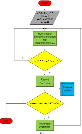
Fig. 3(f) flow chart illustrates how PPV-Icomp empirical non-linear relation is extracted. The model runs for the proposed scheme
as shown in figure. Solar irradiance is varied as steps of 10W/m2 leading to PPV variations from 0 to rated panels power. Vdc is
recorded via hysteresis comparator to generate the required Icomp that leads Vdc to be in a tolerable range around. At each PPV
level, the corresponding Icomp that ensures Vdc approaching the reference is recorded. Finally, a matrix of PPV-Icomp is achieved.
The obtained PPV-Icomp data can be implemented in system simulation/experimental setup as a look-up table. For more enhanced
operation, the same procedure can be repeated considering variable atmospheric temperature, grid harmonics, measurement
errors, etc.. as much as the designer wants the system to be robust. The resultant data can be utilized as off-line training sets for
the suggested ANN.
Both the conventional and the proposed control techniques utilizes similar Proportional-Resonant (PR) controller for the grid
current control, i.e. the VSI main controllable variable. The output of the grid current control PR controller is a sinusoidal signal;
nature of PR controllers that deals with sinusoidal signals, having the same grid voltage frequency with amplitude varies to
ensure grid current convergence to its reference. Hence, the grid current output control signal is utilized as the modulating signal
Vmsin for the VSI SPWM generation. For fixed amplitude carrier signal Vmtri, the VSI modulation index ma varies linearly with
the grid current PR controller output signal Vmsin
.
For over-modulation prevention purpose, a simple limiter is added followingthe PR controller block that limits the modulation index exceed unity as illustrated in fig.2(a) and fig.3(a)
V. Optimal DC-link Voltage
For most appropriate DC-link voltage level determination, the considered system is simulated once using the conventional
control technique and again using the proposed DC-link voltage sensorless technique, for different DC-link voltage levels, under
varying irradiance.
Regarding the first case with the conventional technique, the steady-state performance (regarding THDi and grid power
losses) is presented for four Vdc values at different irradiance levels as shown in fig. 4 parts (a) and (b). The DC-link voltage
value directly affects the converter loss and contributes as well in the grid current THDi level. For Vdc=300V i.e.ma>1, THDi
13
Moreover, for the same irradiance level (i.e. fixed PPV), as Vdc increases, system loss increases. The latter decreases the net
power capable to be transferred to the grid, as shown in fig. 4(b). Hence, under the conventional technique, the best compromise
between power loss and THDi occurs at Vdc=320V where ma ≈1.
Regarding the second case with the proposed sensorless technique, steady-state results (regarding grid currentTHD and grid
power losses) are presented at variable irradiance levels, for the uncompensated scheme as well as the compensated scheme for
two DC-link voltage levels, as shown in fig. 4 parts (c) and (d). Regarding the uncompensated scheme, Vdc will reach about
305V which is less than (311V) as explained before. Although, this will decrease the grid average power losses due to Vdc
level decrease, while the harmonics level in the grid current will exceed the permitted level according to IEEE Std. 519 as ma>1.
Considering the compensated scheme, the system performance is almost similar to that acquired by the conventional DC-link
voltage sensored technique regarding the THDi and grid power losses. Consequently, for the proposed technique with the
compensated scheme, the best compromise between the THDi and grid power losses occurs at Vdc=320V same as for the
conventional scheme. This proves the validity and feasibility of the proposed DC-link sensorless technique with the proposed
system losses compensation scheme.
[image:13.612.88.521.349.649.2]
(c) (d)
Fig. 4: Steady-state results at varying irradiance levels for different DC-link voltage values regarding (a) Conventional technique’s grid currentTHD, (b) Conventional technique’s power losses as percentage of the relative PV power at the current irradiance level, (c) Proposed technique’s grid current THD and (d) Proposed technique’s grid power losses as percentage of the relative PV power at the current irradiance level.
(a) (b) 0%
20% 40% 60% 80%
400 600 800 1000
%
T
H
D
i
Irradiance (W/m2)
Vdc=300V Vdc=320V Vdc=400V Vdc=500V 0% 5% 10% 15% 20% 25% 30%
400 600 800 1000
% G ri d p o w er l o ss es
Irradiance (W/m2)
Vdc=300V Vdc=320V Vdc=400V Vdc=500V 0% 2% 4% 6% 8% 10% 12% 14% 16%
400 600 800 1000
%
T
H
D
i
Irradiance (W/m2)
Uncomp Comp, Vdc=320V Comp, Vdc=400V 0% 5% 10% 15% 20%
400 600 800 1000
% G ri d p o w e r lo ss e s
14
VI. Simulation Results Analysis
In this paper, the transient and steady-state performance of the conventional scheme is compared to that of the proposed one,
under two step changes in irradiance; from 1000 W/m2 to 600 W/m2 at 6s then from 600 W/m2 to 800 W/m2 at 9s.
Both schemes are capable of adjusting the DC-link voltage at 320V during different irradiance levels as shown in fig. 5 parts
(a) and (b) as well. However, injected grid powers, achieved by both schemes, experience losses as shown in fig. 6 parts (a) and
(b), due to converter losses besides the DC-link capacitor parasitic resistance. The DC-link voltage stabilizes at 320V under both
control schemes.
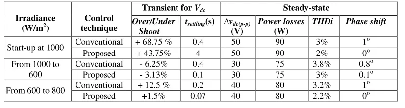
At start-up (fig. 5 (c), and fig. 6 (c)), Vdc overshoot in the conventional technique is about 1.6 times that of the proposed one,
thus Cdc of the former must handle this voltage increase. On the other hand, Vdc adjustment takes much more time, in the
proposed scheme, which increases transient power losses. However, once the required Vdc level is reached, the proposed scheme
shows faster transient response during irradiance changes owing to DC-link voltage controller elimination. This can be shown as
follows;
During the first step change in irradiance, at t=6s, irradiance decreases from 1000 W/m2 to 600 W/m2, thus PPV will decrease
causing a transient decrease in Vdc till it is regulated to 320V. Analysing fig. 5(d), and fig. 6(d), the conventional scheme shows
slower response by about 0.3s. Furthermore, during the conventional scheme's longer transient period, Vdc decreases to 300V
(6.3% Vdc undershoot) i.e. ma >1, thus THDi will go beyond acceptable limits nearly 31.42 %. On the other hand, the proposed
technique shows better response with settling time (ts) of 0.1s and transientdecrease in Vdc to 310 V i.e. ma≈1. Hence, its THDi
is within limits (6.3%) during proposed scheme's transient period. During the second step change at t= 9 s, irradiance increases
from 600 W/m2 to 800 W/m2, thus PPV increases causing transient increase in Vdc. Considering fig. 5(e) and fig. 6 (e), the
conventional scheme exhibits settling time of about 0.2s to reach its steady-state and experiences transient Vdc increase to 360 V
(12.5% Vdc overshoot). On the contrary, during this step change, the proposed scheme shows faster response with ts of almost
0.07s and experiences nearly non-significant Vdc increase during its transient period.
Steady-state results are shown in Table II, include peak-peak DC voltage ripple, THD and power factor of grid current, and
utility power losses for both schemes.
TABLEII. TRANSIENT AND STEADY-STATE PERFORMANCE PARAMETERS OF THE CONVENTIONAL AND PROPOSED SCHEMES REGARDING SIMULATION RESULTS
Irradiance (W/m2)
Control technique
Transient for Vdc Steady-state
Over/Under Shoot
tsettling(s) ∆vdc(p-p)
(V)
Power losses
(W)
THDi Phase shift
Start-up at 1000 Conventional + 68.75 % 0.4 50 90 3% 1 o
Proposed + 43.75% 4 50 90 2% 0o
From 1000 to 600
Conventional - 6.25% 0.4 30 75 3.8% 0.8o
Proposed - 3.13% 0.1 30 75 3% 0.1o
From 600 to 800 Conventional + 12.5 % 0.2 40 80 3.2% 1 o
[image:14.612.104.517.634.744.2]15
(a) (b)
[image:15.612.52.563.101.339.2](c) (d) (e)
Fig. 5: DC-link voltage, at the considered varying irradiance conditions, acquired by (a) conventional technique (b) proposed technique, with a magnified view for each zone at (c)1000 W/m2, (d) 600W/m2, (e) 800 W/m2
(a) (b)
(c) (d) (e)
Fig. 6: Average grid power, at the considered varying irradiance conditions, acquired by (a) conventional technique (b) proposed technique, with a magnified view for each zone at (c)1000 W/m2, (d) 600W/m2, (e) 800 W/m2
[image:15.612.50.558.384.593.2]16
VII. Experimental Implementation
An experimental setup, for the system under investigation, is implemented in order to hold a practical comparison between
the proposed sensorless technique and the conventional one.
For fair comparison, it's mandatory to test these techniques under controlled conditions of irradiance and temperature. This
ensures similar environmental conditions for both techniques when the tests are carried out. Furthermore, it enables the
achievement of a step-change in environmental conditions to compare the transient performance of both techniques.
However, this is inapplicable for rooftop mounted PV panels as they are unable to reproduce similar P-V curves due to the
randomly fluctuating environmental conditions. Thus, the need of solar array simulators to replace actual PV panels arises.
These are expensive instruments and not always affordable thus a simpler solution of simulating I-V and P-V curves similar in
nature to those generated by a PV panel is presented in [61].
Hence, a simple low-cost PV simulating circuit is utilized which employs a resistor bank (Rs) in series with a DC power
supply and the MPPT tracker (boost chopper) is connected at its output as shown in Appendix 3 fig. A.1(a). This circuit
produces a P-V curve that exhibits a peak point for the tracker to lock on. Moreover, it simulates the PV source when exposed to
sudden step change in irradiance. When the switch S is off, Rs becomes only one resistance of R value and this will give a
certain P-V curve. However, when S is closed, Rs becomes in the form of two resistances in parallel (R/2) which will result in a
step increase in the current I and in turn increases the power level, as shown in fig. A.1(b). MPPT is carried out by the first
chopper stage which is followed by the second inverter stage to achieve coupling with the grid. Fig. A.1(a) shows the schematic
diagram of the experimental rig while fig. A.1(d) shows the implemented test rig photography. The selection of the DC-link
voltage to be 36V dc is performed for the experimental setup, similar to the procedure undertaken in the simulation section,
based on acceptable THD in the grid current and reduced system loss as illustrated in Appendix 3 fig. A.2.
In the simulation section: the authors utilize 10 PV panels as the renewable energy source with the specifications listed in
Appendix 1 Table I.
The grid voltage is single phase at 220V rms. The peak injected PV power is 10panels*135W each = 1350 W. The DC-link
voltage was tested for various values from 300V to 500V as illustrated in section V (Optimal DC-link voltage, fig. 4). It was
proofed that the most adequate DC-link voltage value is at 360V from the grid current THD due to over-modulation avoidance.
Hence the simulation results were performed at 360V DC-link as illustrated in Section IV (Simulation results, fig. 5 and fig. 6).
In the experimental validation section:
Due to experimental limitations, it was difficult to construct a roof-mounted system of 10 PV panels. Moreover, the proposed
DC-link voltage sensorless technique needs to be attested during transient and steady-state conditions. For fair comparison with
17
are implemented which is neither controllable nor guaranteed in the case of roof-mounted system as it is subject to unpredictable
solar irradiance and temperature. Hence, the PV emulator, described in the Appendix 3.
The DC power supply, used in the PV emulator, capability is 28V 5A maximum. The constructed circuit runs the DC source at
28V where this voltage is equally distributed between the series power resistor and the DC/DC converter input. Hence the input
to the MPPT tracker is 14V dc. A 22:220V single phase transformer is utilized as a grid interfacing for voltage lifting up.
The authors performed the experimental setup as 10:1 scaled version of the simulated one as illustrated in the following table:
TABLEIII. INCONSISTENCY OF SIMULATION AND EXPERIMENTAL SYSTEMS EXPLANATION Simulation parameters Experimental parameters
Source nature 10 PV panels each is 135W at STC PV emulator with 140W maximum power
Source simulated power 1350W, 713W, 983W 126W, 70W
Source power variation Changing the irradiance level in the simulation file (impossible to guarantee similar performance experimentally)
Manual operated by-pass switch, decreasing the resistance in series
with the DC source which
consequently change the delivered power
DC/DC converter input voltage 180V dc 14V dc
DC/DC converter output voltage (input to VSI)
360V dc 36V dc
DC/AC inverter output rms voltage 220V (Directly connected to a 220V grid)
22V (connected to a 220V grid via 22:220V step up transformer)
Appendix 3 illustrates the actual parameters of both the simulation and the experimental setup.
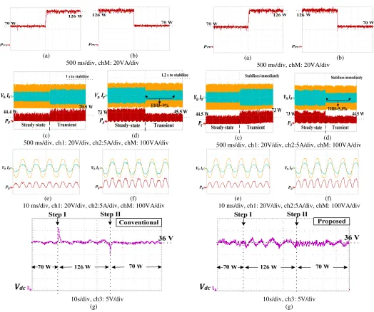
Both techniques' practical results are presented and analysed at Vdc=36 V and under the two step-changes in the input power
from the PV simulator (first from 70W to 126W, then from 126W to 70W).
Two step changes are applied to compare between the transient performances of both techniques. This can be explained as
follows; during the two step changes, both the conventional and the proposed control techniques; are capable of extracting PV
simulator maximum power at both power levels as shown in fig. 7 parts (a) and (b), and fig. 8 parts (a) and (b). However, the
conventional scheme takes longer time to stabilize Vdc at 36V as demonstrated before. During the first step change (from low to
high power level), the conventional scheme exhibits a Vdc increase to 41V (overshoot of 13.9%) then takes almost 1 s to stabilize
Vdc at 36V. This causes a decrease in the grid power, during this transient period, of about 3% than its steady-state value at high
power level (73W) as shown in fig. 7 (c). This transient decrease in grid power occurs in order to compensate for the converter
loss in addition to Cdc losses as the transient Vdc increase to 41V. During the second step change (from high to low power level),
the conventional technique experiences Vdc decrease to 32 V (undershoot of 11.11%) and takes almost 1.2 s to stabilize Vdc at
36V. This, in turn, increases the grid power, during this transient period, of about 2.5% than its steady-state value at low power
level (44.4W) as shown in fig. 7(d). However, during this transient period, the grid current suffers from high THDi beyond the
[image:17.612.39.529.193.365.2]18
proposed technique, immediately adjusts the DC voltage to its required value (36V) and sustains the grid power to its
steady-state value during high power level (73W) and during low power level (44.5W) as shown in fig. 8 parts (c) and (d). During the
second step-change, unlike the conventional technique, the proposed scheme exhibits transient grid current of 5.3% THD.
At steady-state, both schemes succeed in extracting PV simulator maximum power at low PV power level (70W) and at high
PV power level (126W). At the grid side, the steady-state grid powers achieved by both techniques are similar during low grid
power level (about 44.5W) as shown in fig. 7(e) and fig. 8(e); as well as at high grid power level (about 73W) as shown in fig.
8(f) and fig. 8(f). In addition, both schemes achieve near-unity power factor at both power levels and that their exhibited grid
power oscillates around double the line frequency (100 Hz).
(a) (b)
500 ms/div, chM: 20VA/div (a) (b) 500 ms/div, chM: 20VA/div
(c) (d)
500 ms/div, ch1: 20V/div, ch2:5A/div, chM: 100VA/div
(c) (d)
500 ms/div, ch1: 20V/div, ch2:5A/div, chM: 100VA/div
(e) (f)
10 ms/div, ch1: 20V/div, ch2:5A/div, chM: 100VA/div
10s/div, ch3: 5V/div (g)
(e) (f)
10 ms/div, ch1: 20V/div, ch2:5A/div, chM: 100VA/div
10s/div, ch3: 5V/div (g) Fig. 7: Conventional technique performance: PV power; Grid voltage,
current, and power at (a), (c): step change I and (b), (d), : step change II, and steady-state grid voltage, current, and power at (e): low power level and (f): high power level
[image:18.612.49.573.224.662.2] [image:18.612.52.309.232.658.2]19
Fig. 7(g) and Fig. 8(g) show the DC-link voltage adjusted by both techniques at 36 V during both step-changes. During the first
step-change, the conventional technique is slower to stabilize Vdc(tsettling=1s) and experiences an overshoot of about 5V (13.9%)
which will increase the transient grid losses. During the second step-change, similarly, the conventional scheme shows poorer
transient response with settling time of about 1.2s and Vdc undershoot of almost 4V (11.11%). The latter would affect THDi
during this transient period. On the other hand, the proposed technique shows fast transient response during both sudden
changes.
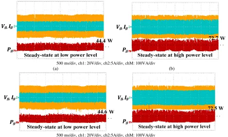
For more clarification regarding the steady-state, fig. 9 illustrates a zooming on the system performance under the conventional
and the proposed technique both tested at low and high power levels. It can be remarked that the proposed control technique
succeeded in attaining the same steady-state performance of the conventional technique with the merit of being DC-link voltage
sensorless control based.
500 ms/div, ch1: 20V/div, ch2:5A/div, chM: 100VA/div
(a) (b)
500 ms/div, ch1: 20V/div, ch2:5A/div, chM: 100VA/div
[image:19.612.72.541.278.561.2](c) (d) Fig. 9: Steady state performance for the investigated system featuring Vg, Ig, and Pg for: (a, b) Conventional control technique (c, d) proposed control technique
20
VIII. Parameters’ Sensitivity Analysis
As the proposed technique is DC-link voltage sensorless based, to what extend the proposed technique is tolerant to system
parameters’ variation is a critical issue to be investigated. This subsection investigates the system performance under
measurement errors and system parameters variations for both conventional and proposed techniques.
A. Measurement error sensitivity analysis
In this subsection, eight simulation runs have been performed. At each simulation run, an error of 5% in the measurement of
Vpv, Ipv and Ig is performed on-purposed in addition to another simulation run with the grid voltage distorted with 5th
harmonic with 5% rms of the fundamental. Similar conditions were performed for the conventional DC-link control
technique.
The DC-link voltage simulation results of both the conventional and the proposed techniques are compared in the following
table with Ppv variations as follows: 1000 W/m2 from 0s to 6s, 600W/m2 from 6s to 9s, and 800 W/m2 from 9s to12s
TABLE IV: Comparison between conventional and proposed techniques’ performance under signal measurement errors
Proposed technique
Conventional technique
Vdc
(V)
Time (s)
Normal case
21
Vdc
(V)
Time (s) Vdc
(V)
Time (s)
5% error in Ipv measurement
Vdc
(V)
Time (s)
5% error in Ig measurement
5th harmonic with amplitude
of 5% of the fundamental in
Vg measurement
It can be noticed that the effect of the measurements’ error on the conventional technique is minimal, which was expected
due to the dedicated DC-link voltage control loop.
The proposed technique, as it mainly depends on the empirical PPV-Icomp relation, the deviation in Vpv and Ipv
measurement causes an error in estimating the actual required compensating current which consequently leads to a
deviation of the DC-link voltage from the desired value, 400V in the above simulated case. But the encouraging thing that
the deviation from the DC-link reference does not exceed 25V from a 400V reference, hence less than 6.3% DC-link
voltage error for a 5% deviation of the Vpv and Ipv measurement. Same results are obtained in case of Ig for 5% deviation
measurement.
Referring to famous LEM® voltage/current sensors LV-25P [62] and LA-55P [63], the guaranteed maximum error in
reading is 0.9% for the voltage and 0.65% for the current.
Although the carried simulations were performed with 5 times the guaranteed error in measurements sensor practical
22
low, hence the effectiveness and tolerance of the proposed system against measurement deviations is validated by worst
case scenarios rigours simulation.
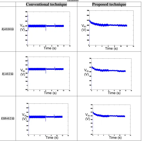
B. Converter parameters sensitivity analysis
In this section, three main factors that affect the inverter loss are varied from their nominal values to study their effect on
the system performance. Those factors are: Output grid side inductor filter resistance, the DC-link capacitor ESR resistance,
[image:22.612.63.554.236.724.2]and the inverter MOSFET on-state resistance. The flowing table illustrates the simulation results
TABLE V: Comparison between conventional and proposed techniques’ performance under converter parameters’ variations
Proposed technique
Conventional technique
Rf=0.04 Ω
Rf =0.2 Ω
23 ESR=0.4 Ω
Ron=0.1 Ω
Ron=0.5 Ω
A deep investigation of the presented results reveals several facts:
for the conventional technique: the effect of variation of the loss-responsible components is nearly unnoticeable. This result
was expected basically due to the presence of dedicated DC-link voltage controller in the conventional technique.
for the proposed technique: the effect of variation of the loss-responsible components is relatively very limited. This result
was basically unexpected due to the absence of dedicated DC-link voltage controller in the proposed technique.
Hence it needs better understanding why those element variation effect is minimal compared to that was recorded in the
case of voltage/current measurement error as illustrated in the previous subsection.
The main reason that the effect of those parameters have is minimal on the system performance is that the investigated
24
contrary to the error in signals’ measurement which directly affects the proper determination of the compensating current
which have higher impact on the system performance.
Therefore, the authors performed rigours investigation, specially from manufacturer data sheets, to reveal the real variation
of the above investigated parameters to avoid any inaccurate parameter values estimation.
Considering Ron, referring to ON Semiconductors® (formerly Fairchild®), considering the power rating of the system under
investigation, one can utilize FCPF150N65F N-channel MOSFET 650V 24A [64], it was found that the on-state resistance
is typically 0.133 Ω and increased by factor 1.7 at 1000C, reaching 0.22. In the investigated simulation, the authors vary Ron
from 0.1 Ω to 0.5 Ω, i.e 5 times greater than the expected values from the manufacturer data sheet.
Considering Rf, referring to HAMMOND
®
, one can utilize 195G10 5mH 10A power inductor [65] as the VSI output filter,
it was found that the inductor internal resistance is typically 0.04 Ω. In the investigated simulation, the authors vary Rf from
0.04 Ω to 0.2 Ω, i.e 5 times greater than the rated values from the manufacturer data sheet.
Considering ESR, referring to Cornell Dubilier CDE®, considering the power rating investigated, one can utilize 300µF 450V DC power capacitor [66] as the VSI DC-link capacitor, it was found that the capacitor ESR is typically 0.268 Ω. In
the investigated simulation, the authors vary ESR from 0.2 Ω to 0.4 Ω, i.e 2 times greater than the rated values from the manufacturer data sheet.
As it can be concluded, the investigated parameters variations, even under the worst case scenarios, has minimal effect on
the system performance under the proposed technique due to their relatively small contribution to loss compared to the
25
IX. Conclusion
This paper proposes an enhanced performance DC-link voltage sensorless control technique for the grid interface of
single-phase two-stage PV converters. This new technique eliminates the need of an outer DC-link voltage control loop. Alternatively,
a new reference grid current generation method is presented to transfer the PV power to the grid. Thus, power balance is
achieved at the DC-link and DC voltage stabilizes at a predetermined level. Consequently, system implementation is simplified
and the control scheme complexity is minimized. Furthermore, the absence of the DC-link high voltage sensor reduces the
system footprint and cost. Although the proposed technique needs system training and mapping between PV power and system
losses, yet the outer loop controller, in the conventional technique, must be precisely tuned to limit THDi. Simulation results of
both schemes are analysed and compared. The proposed technique takes longer time to stabilize the DC-link bus voltage at
operation start-up. However, once the required DC-link voltage is reached, it shows better transient response during sudden
irradiance changes. At steady-state, both techniques give close results, which proves the feasibility of the proposed technique.
Experimental results validate the proposed sensorless scheme effectiveness and show its superiority regarding the transient
response concurrently with its similarity regarding steady-state performance when compared to conventional technique. TABLE
VI lists a comparison between the proposed control technique with recent PV grid connected control schemes from recent
26 where--- not clarified in the corresponding reference.
* Due the bulky grid interfacing transformer impedance which does not exist in case of practical string PV system
References Simulation/ Experimental Work
System Configuration
Control Scheme Power level
Vdc fsw(i) AC
filter
THDi ζ
[17] Simulated System
Single-phase Single- stage grid-tied PV array
(VSI)
--- 6 kW
(220V)
400V 20 kHz L --- 95.7%
Single-phase Two- stage grid-tied PV array (boost chopper +VSI)
--- 6 kW
(220V)
400V 20 kHz L --- 95.5%
[29] Experimental prototype
Single-phase Two- stage grid-tied PV array (ZVT
interleaved boost chopper +VSI )
Sensorless MPPT with PI DC voltage controller
and PI grid current controller
2 kW (220V)
380V 20 kHz L 3.38% 87%
[31]
Simulated System
Single-phase single stage grid-tied PV array
(VSI) Voltage-sensorless One Cycle Control 2kW (230V)
600V 20kHz L --- 81%
Experimental prototype
Single-phase single stage grid-tied Agilent
E4360A Solar Array Simulator. Voltage-sensorless One Cycle Control 205W (30V)
118V 20kHz L 6% 78%
[37] Experimental prototype
Single-phase single stage grid-tied PV array
(proposed Inverter topology)
Grid current PI controller
4.5 kW (230V)
375-537 V
16 kHz LC 2% 98%
for Vdc =375 V
[50] Simulated Experimental prototype
Single-phase grid-tied PV inverter (VSI)
Grid current non ideal PR controller
3 kW (150V)
300V 10kHz LCL 8% ---
[55] Experimental prototype
Single-phase two-stage grid-tied PV system (Boost chopper + VSI)
Grid current PR integral (PRI)
controller
150 W (230/15V)
40V 40kHz L 4.97% ---
[56] Simulated and Experimental prototype
Single-phase single stage grid-tied PV array
(VSI) Grid current Optimal PR controller 1.5kW (220 V)
600V 15kHz LCL --- ---
[58] Experimental prototype
Three-phase single stage grid-tied PV emulator
(Amrel SPS-800-12-D013), (VSI)
Grid current non ideal PR controller with modified harmonic compensator 3.2 kW (200V)
650V 10 kHz LCL 1.5% 84%
Proposed
Simulated System
Single-phase Two stage grid-tied PV string (Boost Chopper + VSI)
Proposed sensorless technique with grid current ideal
PR controller
1.5 kW (220V)
320V 15kHz L 2% 93%
Experimental prototype
Single-phase Two stage grid-tied PV emulator (Boost Chopper + VSI)
Proposed sensorless technique with grid current ideal
PR controller
150 W (220/22V)
27
Acknowledgment
The authors gratefully acknowledge both Renewable Energy and Power Electronics Applications (REPEA) research centre at
28
Appendix 1
A. Boost converter design
In this work, the applied step-up chopper is a single-switch boost converter [35]. It amplifies the PV input voltage level with
a gain given as [36];
,S''*6='/ / =
-O =
1
1 − US''*6 (V. 1)
where VPVis the PV string voltage, Vdc is the DC-link mean voltage and Dboost is the chopper duty ratio. The inductance of the
boost converter (Lboost) is determined by selecting acceptable current ripple passing through it (∆IL) from (A.2):
∆Y=ZUS''*6-O *[(S)\S''*6=
US''*6(1 − US''*6)
Z*[(S)\S''*6 (V. 2)
where fsw(b)is the switching frequency of the boost converter.
B. Decoupling capacitor selection
The high voltage DC-link capacitor, which is the main limiting factor of the inverter lifetime, should be kept as small as
possible and preferably substituted with film capacitors [8]. However, it must be properly sized, to limit DC-voltage ripples to a
desired value in order to prevent over-voltages on the DC-bus and minimize power oscillations whose effect is reflected in the
grid current. DC-link capacitor value is selected according to equation (A.3) neglecting converter losses [8, 37]:
=
∆(()=
2∆ (V. 3)
where Pg is the average active power injected into the grid,ωis the line angular frequency in rad/s,∆(() is the peak to peak
DC-link voltage ripple and∆vdc is the amplitude of the DC-link voltage ripple.
C. Full Bridge VSI
The second stage involves a current controlled full-bridge single-phase VSI operating with sinusoidal pulse width
modulation (SPWM) featuring carrier frequency of 15 kHz. The inverter output filter inductor (Lac) is designed so as to limit the
magnitude of the switching harmonics in grid current. For high switching frequency and near-unity power factor operation, the
inverter output voltage is approximately equal to the grid voltage and the modulation index amplitude (ma) is given by [38, 39]:
M=
(V. 4)
where is the grid voltage amplitude.
For single-phase inverters, Vdc level is determined such that M≤ 1 so as to achieve acceptable total harmonic distortion in
29 ∆=2Z
*[()\
1
2√3]12 M−3π M8 _+38 M` (V. 5)
where ∆Ig is the rms ripple component of the grid current and fsw(i) is the switching frequency of the inverter. ∆Ig can be
calculated from (A.6) [39]:
abU =∆
(&)× 100 ≤ abU (defJde) (V. 6)
where Ig(1) is the rms value of fundamental frequency component of the grid current.
Nominal Short Circuit Current ISCn 8.37A
Nominal Open Circuit Voltage VOCn 22.1V Maximum Power Current IMPP 7.63A Maximum Power Voltage VMPP 17.7V
Maximum Output Power Pmax 135W
Current /Temp. Coefficient Ki 5.02e-3A/oC Voltage/Temp. Coefficient Kv -8e-2V/oC
Number of Series Cells 36
TABLEI.KD135SX_UPUMODULE SPECIFICATIONS AT 25O
[image:29.612.216.454.255.357.2]30
Appendix 2
DC-link voltage and grid current controllers design procedure
For the conventional technique:
The conventional technique features a DC-link voltage controller, basically Proportional-Integral (PI), which is optimized for enhanced performance.
The system runs with Kp only presented by small value with Zero integral part. The value of Kp gradually increases till a sustained oscillation in the Vdc is noticed. The corresponding critical gain Kp-critical and oscillating period Tcritical are recorded. Famous Ziegler - Nichols PID tuning table is utilized for obtaining the utilized PI parameters. For more enhanced performance, a new added block in the Matlab/Simulink R2014 environment which is PID controller with auto-tuning and anti wind-up features is utilized to evaluate the final DC-link voltage PI parameters. Those parameters are used in the experimental setup by means of the embedded code generator library C2000 for the implemented DSP TMS320F28335. Hence, parameters optimization is ensured in both simulation and experimental results. The following figure illustrates the DC-link voltage controller parameters’ tuning process.
For the proposed technique:
The proposed technique features only a conventional Grid current Proportional-Integral controller similar to that utilized in the conventional technique. The DC-link voltage stabilization is achieved naturally when the converter fulfils the adequate required power balance as illustrated in the manuscript.
The following table lists the parameters for the designed grid current PR and DC-link voltage PI controllers respectively Conventional technique Proposed technique
Kp Ki Ts ω Kp Ki Ts ω
31
Start simulation with Kp=0.001 While the Integral
part is zero
Increment Kpuntil
Vdcshows
sustained oscillations
hence Kp-criticalis
reached, record the oscillation
period Tcritical
Start auto-tune process
Start simulation with final auto-tuned controller
variables
Utilize in the embedded C2000
32
Appendix 3
Experimental setup details
(a) (b)
(c) (d)
A.1: Experimental validation (a) experimental system configuration, (b) P-V, I-V curves of PV experimental emulating circuit for two different values of Rs, (c) PPV-Icomp experimental mapping for various DC link voltage values, and (d) test rig photography
(a) (b)