Diffraction grating characterisation for cold-atom
experiments
J. P. M
CG
ILLIGAN, P. F. G
RIFFIN, E. R
IIS ANDA. S. A
RNOLD∗11Dept. of Physics, SUPA, University of Strathclyde, Glasgow G4 0NG, UK *[email protected]
Compiled April 25, 2016
We have studied the optical properties of gratings micro-fabricated into semiconductor wafers, which can be used for simplifying cold-atom experiments. The study entailed characterisation of diffraction efficiency as a function of coating, periodicity, duty cycle and geometry using over 100 distinct gratings. The critical parameters of experimental use, such as diffraction angle and wavelength are also discussed, with an outlook to achieving optimal ultracold experimental conditions.
OCIS codes: (140.3320) Laser cooling; (140.7010) Laser trapping. (050.1950) Diffraction gratings. (050.1960) Diffraction theory. http://dx.doi.org/10.1364/josab.XX.XXXXXX
1. INTRODUCTION
Cold atom technologies have dominated precision measure-ments in recent years [1–4]. The preference for cold atoms arises from the increased interrogation time that is provided in an iso-lated environment, allowing higher precision to be taken from a measurement [7]. Although many metrological experiments ben-efit from cold atom measurements [8,9], the standard apparatus required is typically too large for portable devices. Despite the fact that current miniaturised metrological devices have proven highly successful [10], their precision and accuracy is limited by their use of thermal atoms.
The source of cold atoms in most experiments is a standard magneto-optical trap (MOT) [11,12] which utilise 6 indepen-dent beams, each with their own alignment and polarisation optics. We have previously demonstrated a device that collects cold atoms in an optically compact geometry using a grating magneto-optical trap, GMOT [13, 14], which is an extension of the equivalent MOT using a tetrahedral reflector [15]. Such MOTs are grating/mirror variants of the original 4-beam MOT by Shimizuet al.[16]. The simple design of the GMOT reduces the standard 6-beam MOT experimental set-up to one incident beam upon a surface-etched, silicon wafer diffraction grating. The grating uses the incident light and first diffracted orders to produce balanced radiation pressure, allowing us to trap a large number of atoms at sub-Doppler temperatures [14,17]. This greatly reduces the scale and complexity of optics used in laser cooling apparatus to facilitate applications [18–20].
In this paper we present a detailed optical characterisation of these micro-fabricated diffraction gratings, with a view to aid-ing future cold atom quantum technologies. Comparisons are made with basic theoretical models of the light diffracted from
binary periodic diffraction gratings. This study will be aimed to-wards an understanding of how metal coatings, periodicity, duty cycles and geometry affect the diffraction efficiency, a crucial parameter for creating balanced radiation pressure. Finally, we discuss additional parameters that have proven critical during our studies.
2. THEORY: DIFFRACTION GRATINGS
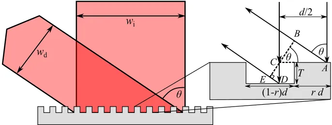
Previous efforts made towards producing a reliable theory of diffraction require a typically complex derivation of Maxwell’s equations [5,6]. However, significant insight into the optical performance of our MOT gratings can be obtained from a sim-plified theory for determination of the first and zeroth order diffraction efficiencies. We would like to draw attention to the optical theory expounded in Ref. [22], and use the same notation throughout this paper for convenience in comparison. However, here we use an even simpler phasor-based version of the theory which gives a surprisingly good agreement to experiment. Note also that the zeroth order is calculated via an alternative method. The diffraction gratings considered in this work are com-posed of a combination of reflecting elements arranged in a periodic array, separated by a distance comparable to the wave-length of study, and alternate elements etched into the surface as seen in Fig. 1. This structure is directly analogous to transmissive classical slits [21].
θ
B
w
iw
dT
d
/2
θ
θ
A
C
D
E
[image:2.612.131.474.45.174.2](1
-r
)
d
r d
Fig. 1.Surface of a binary diffraction grating of etch depthT, diffraction angleθ, perioddand duty cyclerand 1−rfor trough and peak respectively.
equation simplifies to the Bragg condition,
mλ=dsinθ, (1)
whereθis now the angle of diffraction.
Fig. 1 shows how the total electric field can be represented as the sum of diffracted orders from the trough and peak of the grating, which are weighted by their relative sizes(1−r)d=rcd andrd, respectively and phase shifted by the path difference between AB = d/2 sinθ(= mλ/2 from Eq.1) and CDE = T(1+cosθ), i.e.:
Etot/ρ1/2 ∝ (r+rceiφ) (2)
where φ = 2π λ
(mλ/2−T(1+cosθ)),
whereTis the etch depth,λthe wavelength of incident light, andρis the metal reflectivity. This gives a simple ‘phasor’ model of the diffraction efficiency.
Using this electric field, in the case of 50/50 duty cycle,r= rc=0.5, and a 1D grating then the intensity efficiency,η1, in the
first diffracted orders can be calculated via
η1=ρ|1+exp[iπ(1−2T(1+cosθ)/λ)]|
2
8 , (3)
whereρis the reflectivity of the coating metal used, allowing for losses (see more on this in Sec.4).
Eq. (3) now provides a simple relation between the intensity of the light diffracted in the first order relative to the period of the grating. A simple model could thus assume that, for lossless diffraction with no grating orders|m| ≥1, the zeroth order can be described by,
2η1+η0=ρ, (4)
If the etch depth,T, is designed such thatT=λd/4, whereλd is the design wavelength and cosθ≈1 then Eq. (3) simplifies further to,
η1=R
1+exp(iπλd 2λ)
2
8 . (5)
Note that to apply first order diffraction efficiencies,η1, to 2D
gratings we simply multiply by 1/2, to account for twice as many diffracted beams.
To determine how these diffracted efficiencies relate to creat-ing a balanced radiation pressure we must account for the verti-cal intensity balance between the incident,Ii, and the diffracted
orders,Id, described as IIdi =η1
wi
wd =
η1
cosθ, wherewi(Fig. 1) is the incident beam waist andwd is the diffracted beam waist.
The radial balance is not considered as this is automatic if the beam center is positioned on the grating center. The net incident intensity on the gratingIi(1−η0)is ideally balanced with the
component of the diffracted intensity which is anti-parallel with the incident light, i.e.N IdcosθwhereNaccounts for the num-ber of diffracted first orders, which simplifies toN Iiη1. Thus,
for all models the balance between incident and diffracted light, perpendicular to the grating and taking the zeroth order into account, is described mathematically through the dimensionless quantity,
ηB=Nη1/(1−η0) (6)
which is ideally one.
In summary we have used a simple model, adapted from Ref. [22], for zeroth and first order diffraction efficiencyη0and
η1 and thereby the radiation balance ηB. The model uses a
simple two phasor addition (Eqs.3,4) which can be shown to be directly proportional to a more complete phase integral across the grating, but ignoring the effect of shadowing.
3. EXPERIMENT: GRATING CHARACTERISATION
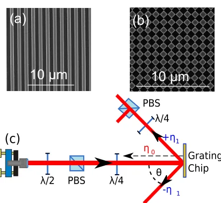
The diffraction gratings used were manufactured with a dry etch into silicon wafers and patterned using electron beam lithogra-phy [23,24] to an ideal etch depth ofh=λd/4 (λd=780 nm) and chosen periodicity. The wafer on which the Au gratings were etched is composed of silicon topped with 10 nm Ti and 20 nm Pt, whereas no adhesion layer was required for an Al grating. These are then sputter coated with a variable thickness coating layer. The geometry of the etch can vary between one dimen-sional, 1D, and two dimendimen-sional, 2D, gratings as illustrated in the scanning electron microscope images in Fig. 2(a) and (b), respectively. The 2D grating produces four first order diffracted terms compared to the two produced in a 1D geometry.
To produce the ideal grating, a thorough investigation of how fabrication parameters affect the diffraction efficiency is required. To determine the optimum settings for future diffraction grat-ings we commissioned the construction of over one hundred 2 mm×2 mm gratings, produced with a variety of periodicity, duty cycles, geometrical layout, coating metal and coating thick-ness. In order to measure the properties of the large quantity of diffraction gratings we constructed a dedicated testing station with incident collimated, circularly polarised light of known wavelength and power, as can be seen in Fig.2.
10 μm
(a)
10 μm
(b)
λ
/2
λ
/4
Grating
Chip
PBS
PBS
λ
/4
+
η
1-
η
1η
0 [image:3.612.61.284.38.242.2]θ
(c)
Fig. 2.(a) (b): Scanning electron microscope images of 1D and 2D gratings respectively. (c): Set-up used for grating efficiency and polarisation purity analysis. Abbreviations areλ/2 and λ/4 for the half and quarter wave-plates respectively, PBS for polarising beam splitter,ηirepresents the relative power in the ithorder of diffraction andθis the angle of diffraction.
discussed later. The position of the diffracted order was noted, andθmeasured. This allowed the periodicity to be inferred through the Bragg condition, Eq. (1). The diffracted order is mea-sured for diffracted power, then passes through aλ/4 plate and PBS to measure any degradation of polarisation that may have occurred during diffraction. The results of this investigation can be seen in Figs.3and4, and in greater detail in their associated Appendix (Sec.8) Figs.7and8respectively.
Fig.3depicts how the relative diffracted power and beam intensity balance vary with diffraction angle,θfor 1D and 2D gratings. The circles and squares represent gratings with spatial dimension etched:unetched duty cycles over one grating period of 60%:40% and 50%:50% respectively. Both data sets provided have a coating of 80 nm Au, however, further investigation was carried out into thicker coatings on Au as well as Al, with both 1D and 2D geometries. The results provided in Fig.3are typical of all data sets recorded. Associated Appendix (Sec.8) Figs.7 and8provide detailed diffraction efficiency and polarisation pu-rity information, respectively, for 1D and 2D gratings with two different thicknesses of gold and aluminium coating. Moreover, Fig.7also shows that – for the 1D gratings – gold with a thin 20nm alumina coating has similar reflectivity to plain gold. The purpose of the alumina coating was to introduce a layer between the Au surface of the grating and the Rb metal vapour inside the vacuum system, which corrodes the Au.
The first point of interest is the decrease of the diffracted order relative to diffraction angle. As the first order decreases, the light in the zeroth order increases at the same rate, maintaining a close to constant total power. This decay is weaker in the gratings with 60%:40% duty cycle, making this the preferable choice to 50%:50% duty cycle. Analysis of experimental data proved that a thicker coating material causes no notable change in the 1D gratings. However, the diffraction efficiency was seen to increase by≈10% when twice the coating thickness was applied to 2D gratings. A gold coating produces a stronger diffracted order than that of the aluminium of similar coating depth due to the
(
a
)
30 40 50 60 70 0
20 40 60 80 100 120 140
θ(deg)
η0
,
η1
,
3
η1
/(
1
-η0
)(
%
)
(
b
)
30 40 50 60 70 0
20 40 60 80 100 120
θ(deg)
η0
,
2
η1
,
4
η1
/(
1
-η0
)(
%
[image:3.612.324.563.50.201.2])
Fig. 3.Diffraction angle vs. radiation balance and diffraction efficiency. (a): 1D gratings with 80 nm Au coating. (b): 2D gratings with 80 nm Au coating. Blue and red represent the diffracted(η1)and reflected(η0)orders respectively, with
black illustrating the radiation balance for gratings with duty cycles of 40%:60% and 50%:50% (circles and squares). The theory models are based on Eqs.3,4(solid curves).
higher reflectivity of gold. The results from the duty cycle are conclusive that 60%:40% duty cycle produces a lower zeroth order and higher diffraction efficiency. The reasoning for this is not completely understood, but further modelling will be provided in Ref. [25].
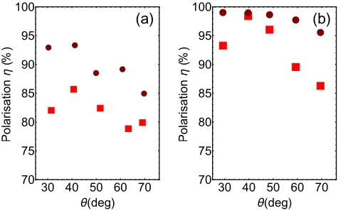
Fig. 3also illustrates the balance of light force from Eq. (6) for the respective geometry of the gratings intended use, as a function of diffraction angle. Axial balance between the incident downward beam and diffracted upward orders is achieved at 100% in Fig.3. This balancing force is notably higher in the 1D gratings compared to the 2D gratings as the 1D gratings only diffract into 2 beams rather than 4. However, with appropriate filtering of the incident beam, this can be overcome to produce well balanced radiation forces [17] required for laser cooling [26, 27]. Using a 4 beam configuration with a linear grating provides close to ideal balance already without need for further adaptations to the apparatus. The results are typical of 1D and 2D gratings. Testing was also carried out on Au coated gratings with a top layer of alumina. Although there was no difference in diffraction efficiency between the gratings with and without the alumina, the additional layer was observed to degrade the polarisation purity of the diffracted order, Fig.4.
(
a
)
30 40 50 60 70 70
75 80 85 90 95 100
θ(deg)
Polarisation
η
(%
)
(
b
)
30 40 50 60 70 70
75 80 85 90 95 100
θ(deg)
Polarisation
η
(%
[image:4.612.320.562.43.191.2])
Fig. 4.Diffraction angle vs. polarisation purity. (a): 1D grat-ings with 80 nm Au and Alumina layer. (b): 1D gratgrat-ings with 80 nm Au. Associated Appendix (Sec.8) Fig.8provides de-tailed polarisation efficiency information for 1D and 2D grat-ings with two different thicknesses of gold and aluminium coating. Fig.8also shows the effect of the 20nm alumina coat-ing for three sets of 1D gratcoat-ing chips. In all images duty cycles of 60%:40% and 50%:50% are indicated by circles and squares, respectively.
4. EXPERIMENT: LOST LIGHT
As has been pointed out with the diffraction efficiency data, the total power measured in the diffracted orders fell short of the incident power by≈18 %. The theoretical reasoning for this can be conceived as shadowing of the beam/diffraction losses in the pits of the grating and is discussed in more detail in [25] – here we discuss experiment measurement of the losses. An initial investigation into the elusive light was carried out through the investigation of the absorption profile of a grating by measuring the transfer of light to heat. For this, a small thermistor was well insulated to the back of a 4 mm×4 mm Au coated diffraction grating, to read out the heating rate of the grating with a known incident laser power. This absorption rate can be seen in Fig.5. To calibrate the grating heating to a known power, Ohmic heating was applied through a 1.5 kΩresistor thermally attached to the back of the grating, separate from the thermistor. This resistor was connected in series to a voltage supply to deposit known amounts of power onto the grating, whilst measuring the heating rate. This Ohmic heating rate was then matched to that of the laser heating to determine the amount of laser power absorbed by the grating during the heating process.
In order to account for thermal gradients in the area of the grating, the measurement procedure was also carried out for a plain Au coated wafer. Since plain Au has a known 3 % ab-sorption at 780 nm [28] we could use this to account for thermal gradients in the measurement area, that could then be applied to the grating data. Applying this correction factor allows us to de-duce that 12±2 % of incident light is absorbed by the diffraction grating.
A further study into the possibility of the missing light be-ing scattered was carried out to see if fabrication imperfections were projecting light into unwanted diffraction angles [29]. This was carried out by taking long exposure images around a 90◦ plane of diffraction and normalising the range of exposure times to determine the relative power in an minuscule peaks found. The data from this provided that<1% of lost light was being
0 20 40 60 80 100
0 2 4 6 8
Time(s)
Δ
T
(
K
[image:4.612.44.285.51.201.2])
Fig. 5.Absorption rate of 1D Au coated grating heated with laser light (red) and calibrated with Ohmic heating (dashed blue).
scattered by the grating.
5. EXPERIMENT: CRITICAL PARAMETERS
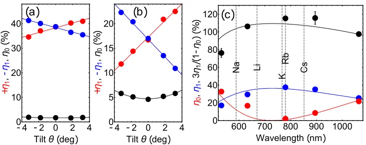
When implementing the diffraction grating into an experimental set-up, it is mounted perpendicular to the incident beam, how-ever, the extent to which this angle of incidence can be varied is an important consideration. We investigated the angle sen-sitivity using the same set-up as in Fig.2(c), with variable tilt applied to the grating mount. Whilst in this configuration, a known amount of light was incident upon the grating, held at a variable tilt angle whilst the diffracted orders where measured. This procedure was carried out for both 1D and 2D gratings, the results of which are seen in Fig.6(a) - (b).
The blue and red data sets represent the opposite first diffracted orders, with black representing the zeroth, with best fitting lines and parabola applied. Fig.6(a)- (b) demonstrates that a small deviation from 90◦will symmetrically imbalance the first diffracted orders, and increase the unwanted zeroth order. This asymmetry vs angle is markedly more for 2D gratings (b) in comparison to 1D gratings (a).
It would also be of importance to know how the diffraction gratings’ diffracted efficiency varies with the wavelength of in-cident light, as a wide bandwidth of wavelengths could unlock alkaline earth metals as possible species to be used in the grat-ing MOT configuration. Additionally, knowgrat-ing the dependence uponλwould also provide understanding of etch depth, where h=λ/4. For this investigation the same set-up was used as in Fig.2, with 5 different lasers, covering a range of wavelengths seen in Fig.6(c). The red and blue data points depict the mea-surements of first and zeroth diffracted orders, with the fits derived from Eq. (5). The black data points again depict the in-tensity balance from Eq. (6). As is illustrated, the grating would deliver reasonably balanced cooling within±200 nm of the de-sign wavelength of 780 nm, and would be useful for cooling a variety of alkali metals.
6. CONCLUSIONS AND OUTLOOK
(
a
)
-4 -2 0 2 4
0 10 20 30 40
Tiltθ(deg)
+
η1
,
-η1
,
η0
(%
)
(
b
)
-4 -2 0 2 4
0 5 10 15 20
Tiltθ(deg)
+
η1
,
-η1
,
η0
(%
)
(
c
)
Na Li
K
Rb
Cs
600 700 800 900 1000
0 20 40 60 80 100 120
Wavelength(nm)
η0
,
η1
,3
η1
/(
1
-η0
)
(%
[image:5.612.124.496.42.190.2])
Fig. 6.Left: The grating angle tilt vs. the power in the relative diffracted orders with simple linear/parabolic fits for (a): Al 1D grating,d= 1478 nm. (b): Au 2D grating,d= 1056 nm. (c): Using the same grating as in (a), the wavelength of incident light is varied and recorded against the powers of first and zeroth diffracted orders and fit against theory from Eq. (5). Black data points represent the intensity balance from Eq. (6). The same set-up as in Fig.2was used, except theλ/4 wave-plates were replaced by Fresnel rhombs due to their achromatic retardance. The alkaliD2line wavelengths typically used for laser cooling are indicated by
dashed vertical lines, showing wide grating versatility.
We conclude that future gratings should be created with a higher duty cycle, as was seen from our study between 50%:50% and 60%:40% duty cycles. The study of coating thickness has also demonstrated that for the 2D geometry the thicker coating metal is preferable for higher diffraction efficiency. If an additional coating of alumina is placed on top of the grating for use within a vacuum system then a degradation of the polarisation purity has been noted. However, the efficiency of the weaker polarisation, with the correct duty cycle, does not hinder the creation of a MOT.
Finally, the critical parameters discussed demonstrate that, when implemented experimentally, the grating should be as close to perfectly perpendicular as possible to maintain balance between the diffracted orders, especially for the 2D gratings. The study of wavelength demonstrates broadband diffractive ef-ficiency, opening the door to the cooling of elements on multiple atomic transitions.
7. ACKNOWLEDGEMENTS AND FUNDING
We are grateful for valuable discussions with Joe Cotter and Ed Hinds. EPSRC (EP/M013294/1); DSTL (DSTLX-100095636R); ESA (4000110231/13/NL/PA); InnovateUK QuDOS.
8. APPENDIX: CHARACTERISING GRATING DIFFRAC-TION AND POLARISADIFFRAC-TION EFFECTS VS. COATING
Please see Figs.7and8after the references.
REFERENCES
1. M. Takamoto, F. L. Hong, R. Higashi, and H. Katori, “An optical lattice clock,”Nature435, 321-324 (2005).
2. C. Deutsch, F. Ramirez-Martinez, C. Lacroûte, F. Reinhard, T. Schnei-der, J. N. Fuchs, F. Piéchon, F. Laloë, J. Reichel, and P. Rosenbusch, “Spin self-rephasing and very long coherence times in a trapped atomic ensemble,”Phys. Rev. Lett.105, 020401 (2010).
3. N. Poli, F. Y. Wang, M. G. Tarallo, A. Alberti, M. Prevedelli and G. M. Tino, “Precision measurement of gravity with cold atoms in an optical lattice and comparison with a classical gravimeter,”Phys. Rev. Lett.106, 038501 (2011).
4. C. Gross, T. Zibold, E. Nicklas, J. Estève, and M. K. Oberthaler, “Nonlin-ear atom interferometer surpasses classical precision limit,”Nature464, 1165-1169 (2010).
5. M. A. Golub and A. A. Friesem, “Effective grating theory for resonance domain surface-relief diffraction gratings,”J. Opt. Soc. Am. A22, 1115-1126 (2005).
6. E. G. Loewen, D. Maystre, R. C. McPhedran and I. Wilson, “Correlation between Efficiency of Diffraction Gratings and Theoretical Calculations over a Wide Range,”J. Appl. Phys.14, 143-152 (1975).
7. S. Bize, P. Laurent, M. Abgrall, H. Marion, I. Maksimovic, L. Cacciapuoti, J. Grunert, C. Vian, F. Pereira dos Santos, P. Rosenbusch, P. Lemonde, G. Santarelli, P. Wolf, A. Clairon, A. Luiten, M. Tobar, and C. Salomon, “Cold atom clocks and applications,”J. Phys. B38, 449-468 (2005). 8. B. J. Bloom, T. L. Nicholson, J. R. Williams, S. L. Campbell, M. Bishof, X.
Zhang, W. Zhang, S. L. Bromley, and J. Ye, “An optical lattice clock with accuracy and stability at the10−18level,”Nature506, 71-75 (2014). 9. M. E. Zawadzki, P. F. Griffin, E. Riis, and A. S. Arnold, “Spatial
interfer-ence from well-separated split condensates,”Phys. Rev. A81, 043608 (2010).
10. P. D. D. Schwindt, S. Knappe, V. Shah, L. Hollberg, J. Kitching, L. A. Liew, and J. Moreland, “Chip-scale atomic magnetometer,”Appl. Phys. Lett.85, 6409-6411 (2004).
11. E. L. Raab, M. Prentiss, A. Cable, S. Chu, and D. E. Pritchard, “Trapping of neutral Sodium atoms with radiation pressure,”Phys. Rev. Lett.59, 2631 (1987).
12. C. Monroe, W. Swann, H. Robinson, and C. Wieman, “Very cold trapped atoms in a vapor cell,”Phys. Rev. Lett65, 1571 (1990).
13. M. Vangeleyn, P. F. Griffin, E. Riis, and A. S. Arnold, “Laser cooling with a single laser beam and a planar diffractor,”Opt. Lett.35, 3453-3455 (2010).
14. C. C. Nshii, M. Vangeleyn, J. P. Cotter, P. F. Griffin, E. A. Hinds, C. N. Ironside, P. See, A. G. Sinclair, E. Riis, and A. S. Arnold, “A surface-patterned chip as a strong source of ultracold atoms for quantum tech-nologies,”Nature Nanotech.8, 321-324 (2013).
15. M. Vangeleyn, P. F. Griffin, E. Riis and A. S. Arnold, “Single-laser, one beam, tetrahedral magneto-optical trap,”Opt. Express17, 13601-13608 (2009).
16. F. Shimizu, K. Shimizu, and H. Takuma, “Four-beam laser trap of neutral atoms,”Opt. Lett.16, 339-341 (1991).
17. J. P. McGilligan, P. F. Griffin, E. Riis, and A. S. Arnold, “Phase-space properties of magneto-optical traps utilising micro-fabricated gratings," Opt. Express 23, 8948-8959 (2015).
18. J. A. Rushton, M. Aldous, and M. D. Himsworth, “The feasibility of a fully miniaturized magneto-optical trap for ultracold quantum technology,” Rev. Sci. Instrum.85, 121501 (2014).
20. R. Szmuk, V. Dugrain, W. Maineult, J. Reichel, and P. Rosenbusch, “Stability of a trapped atom clock on a chip,”Phys. Rev. A92, 012106 (1985).
21. C. A. Palmer and E. G. Loewen, “Diffraction grating handbook,” Spring-field, OH: Newport Corporation (2005).
22. J. P. Cotter, J. P. McGilligan, P. F. Griffin, I. M. Rabey, K. Docherty, E. Riis, A. S. Arnold and E. A. Hinds,arXiv:1601.05548
23. A. A. Tseng, C. Kuan, C. D. Chen, and K. J. Ma, “Electron beam lithography in nanoscale fabrication: recent development,”Electronics Packaging Manufacturing, IEEE transactions26, 141-149 (2003). 24. U. D. Zeitner, M. Oliva, F. Fuchs, D. Michaelis, T. Benkenstein T.
Harzen-dorf, and E-B Kley, “High performance diffraction gratings made by e-beam lithography,”Appl. Phys. A109, 789–796 (2012).
25. J. P. Cotteret al., submitted (2016).
26. S. Chu, L. Hollberg, J. E. Bjorkholm, A. Cable, and A. Ashkin, “Three-dimensional viscous confinement and cooling of atoms by resonance radiation pressure,”Phys. Rev. Lett.55, 48 (1985).
27. J. Dalibard and C. Cohen-Tannoudji, “Laser cooling below the Doppler limit by polarization gradients: simple theoretical models,”J. Opt. Soc. Am. B6, 2023-2045 (1989).
28. V. R. Weidner and J. J. Hsia, “NBS measurement services: spec-tral reflectance,”Center for radiation research, National Measurement Laboratory, NBS, MD 20899 (1987).
30 40 50 60 70 0 20 40 60 80 100 120 140
θ(deg)
η0 , η1 , 3 η1 /( 1 -η0 )( % ) 200nm Al
30 40 50 60 70 0 20 40 60 80 100 120 140
θ(deg)
η0 , η1 , 3 η1 /( 1 -η0 )( % ) 100nm Al
30 40 50 60 70 0 20 40 60 80 100 120 140
θ(deg)
η0 , η1 , 3 η1 /( 1 -η0 )( % ) 180nm Au
30 40 50 60 70 0 20 40 60 80 100 120 140
θ(deg)
η0 , η1 , 3 η1 /( 1 -η0 )( % ) 80nm Au 1D data
30 40 50 60 70 0 20 40 60 80 100 120 140 θ(deg) η0 , η1 ,3 η1 /( 1 -η0 )( % ) 195nm depth
30 40 50 60 70 0 20 40 60 80 100 120 140 θ(deg) η0 , η1 ,3 η1 /( 1 -η0 )( % ) 200nm depth
30 40 50 60 70 0 20 40 60 80 100 120 140 θ(deg) η0 , η1 ,3 η1 /( 1 -η0 )( % ) 170nm depth 1D 80nm Au with Alumina data
30 40 50 60 70 0 20 40 60 80 100 120
θ(deg)
η0 , 2 η1 , 4 η1 /( 1 -η0 )( % ) 200nm Al
30 40 50 60 70 0 20 40 60 80 100 120
θ(deg)
η0 , 2 η1 , 4 η1 /( 1 -η0 )( % ) 100nm Al
30 40 50 60 70 0 20 40 60 80 100 120
θ(deg)
η0 , 2 η1 , 4 η1 /( 1 -η0 )( % ) 180nm Au
30 40 50 60 70 0 20 40 60 80 100 120
θ(deg)
[image:7.612.79.539.91.636.2]η0 , 2 η1 , 4 η1 /( 1 -η0 )( % ) 80nm Au 2D data
30 40 50 60 70 70
75 80 85 90 95 100
θ(deg)
Polarisation
η
(%
)
200nm Al
30 40 50 60 70 70
75 80 85 90 95 100
θ(deg)
Polarisation
η
(%
)
100nm Al
30 40 50 60 70 70
75 80 85 90 95 100
θ(deg)
Polarisation
η
(%
)
180nm Au
30 40 50 60 70 70
75 80 85 90 95 100
θ(deg)
Polarisation
η
(%
)
80nm Au 1D data
30 40 50 60 70 60
70 80 90 100
θ(deg)
Polarisation
η
(%
)
195nm depth
30 40 50 60 70 60
70 80 90 100
θ(deg)
Polarisation
η
(%
)
200nm depth
30 40 50 60 70 60
70 80 90 100
θ(deg)
Polarisation
η
(%
)
170nm depth
1D 80nm Au with Alumina data
30 40 50 60 70 70
75 80 85 90 95 100
θ(deg)
Polarisation
η
(%
)
200nm Al
30 40 50 60 70 70
75 80 85 90 95 100
θ(deg)
Polarisation
η
(%
)
100nm Al
30 40 50 60 70 70
75 80 85 90 95 100
θ(deg)
Polarisation
η
(%
)
180nm Au
30 40 50 60 70 70
75 80 85 90 95 100
θ(deg)
Polarisation
η
(%
)
[image:8.612.83.532.111.640.2]80nm Au 2D data