Phonon Spectroscopy at Atomic Resolution
F. S. Hage,1,* D. M. Kepaptsoglou,1,2 Q. M. Ramasse,1,3,† and L. J. Allen4,5,‡ 1
SuperSTEM Laboratory, SciTech Daresbury Campus, Daresbury WA4 4AD, United Kingdom
2York JEOL Nanocentre and Department of Physics, University of York, Heslington, York YO10 5BR, United Kingdom 3
School of Physics and School of Chemical and Process Engineering, University of Leeds, Leeds LS2 9JT, United Kingdom
4School of Physics, University of Melbourne, Parkville, Victoria 3010, Australia 5
Ernst Ruska-Centre for Microscopy and Spectroscopy with Electrons, Forschungszentrum Jülich, 52425 Jülich, Germany
(Received 26 September 2018; published 10 January 2019)
Advances in source monochromation in transmission electron microscopy have opened up new possibilities for investigations of condensed matter using the phonon-loss sector of the energy-loss spectrum. Here, we explore the spatial variations of the spectrum as an atomic-sized probe is scanned across a thin flake of hexagonal boron nitride. We demonstrate that phonon spectral mapping of atomic structure is possible. These results are consistent with a model for the quantum excitation of phonons and confirm thatZ-contrast imaging is based on inelastic scattering associated with phonon excitation.
DOI:10.1103/PhysRevLett.122.016103
Improvements in monochromation of electron sources and in spectrometer designs mean that an energy resolution of the order of 10 meV or better is now achievable in experimental electron energy-loss spectroscopy (EELS) [1–3]. This allows the details of energy-loss spectra to be observed down to THz frequencies, meaning that vibrational spectra associated with phonon excitations are accessible.
Opening up the phonon-loss sector is of importance in physics and materials science since this will allow detailed studies of bonding arrangements, thermal and optical transport, as well as the detection of hydrogen and other light elements directly in the electron microscope. The atomic-scale focused coherent probe in scanning trans-mission electron microscopy (STEM) allows the vibra-tional information to be obtained from nanometer-sized regions, making it possible to detect localized vibrational excitations and states. There have been several prospective explorations of these possibilities [4–7]and initial exper-imental applications have included the measurement of vibrational modes of an ionic liquid [2], the detection of water and its derivatives on individual nanoparticles [8], and the mapping of vibrational surface and bulk modes in a single MgO nanocube[9]. Further methodological devel-opments have enabled local temperature measurements based on energy gain and loss spectroscopy [10], while momentum-resolved vibrational-loss spectroscopy has recently demonstrated the ability to map both acoustic and optical phonons across the first Brillouin zone of a crystal using a nanometer-sized electron probe[11,12].
Several authors have considered whether phonon scat-tering could give rise to higher resolution signals [6,7, 13–16], taking full advantage of the atomic-sized probe in STEM. This issue has been discussed vigorously since
energy losses in the phonon sector are small (of the order of 1–500 meV for single phonon excitation), implying sig-nificant delocalization. However, as discussed in Ref.[16], atomically resolved vibrational EELS should be possible since atomic resolution high-angle annular dark-field (HAADF) imaging, also known as Z-contrast imaging, detects electrons which have been scattered to large angles after the excitation of phonons, as we will confirm in this Letter.
Dwyer et al. [17] demonstrated, using a specimen of hexagonal boron nitride, that a focused beam of high-energy electrons can map the vibrational modes of a material with a spatial resolution better than two nanometers. Hexagonal boron nitride is a polar dielectric that gives rise to both localized (impact) and delocalized (dipole) electron-vibrational scattering. The dipole scattering gives rise to a background in the images. Dwyer showed that an annular collection geometry should significantly reduce the dipole background, thereby reducing the electron dose required to observe atomic-scale contrast in phonon images[18].
In this Letter, we show that a resolution an order of magnitude better than in Ref.[17]is possible, also using a specimen of hexagonal boron nitride. We demonstrate that electrons in the phonon sector of the energy-loss spectrum provide atomic resolution structure maps of the specimen when the detector is moved off the optical axis and outside the bright-field disk to angular ranges used for typical Z-contrast imaging detection geometries. The variation in such spectra with the probe positioned both on and off atomic columns is investigated and the underlying physics is discussed. The structure maps can only be understood using the quantum excitation of phonons (QEP) model[19] and not in the context of the widely used frozen phonon model[20,21]. The frozen phonon model is often used to
PHYSICAL REVIEW LETTERS
122,
016103 (2019)
modelZ-contrast imaging assuming elastic scattering from different atomic configurations but the results here show unambiguously that it is inelastically scattered electrons, involved in phonon excitation, which form such images.
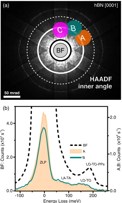
Energy-loss spectra were acquired at an acceleration voltage of 60 kV and a probe convergence semiangle of 31.5 mrad, resulting in a 1 Å probe size, using a Nion UltraSTEM 100MC scanning transmission electron micro-scope, equipped with a Gatan Enfinium ERS EEL spec-trometer. The different detector positionsA–Cindicated in Fig.1(a)were obtained by using a combination of micro-scope postspecimen deflectors to shift the diffraction pattern with respect to the spectrometer entrance aperture (and HAADF detector). The semiangle of the detectors (i.e., the spectrometer entrance aperture) is 22 mrad in each case. More experimental parameters are given in [22].
Figure 1(b) shows low-loss spectra averaged over the detector for three of the geometries indicated in Fig. 1(a) and normalized by the total acquisition time. The signal is clearly much larger for the detector at the bright-field (BF) position than at the off-axis positions (AorB), especially for the zero-loss peak (ZLP). Its full width at half maximum (a commonly used measure of the achieved energy reso-lution) is slightly increased at positionsAandB(52 meV, compared to 28 meV at the BF position) but this is primarily due to a combination of instrumental factors, as discussed in Ref. [11].
More importantly, phonon-loss peaks are clearly observ-able between 50–200 meV: both longitudinal (L) and transverse (T) acoustic (A) and optical (O) phonon branches and surface phonon polaritons (PPs) [11,12]. PPs appear at energy losses between theTOandLObulk modes[11,12,17,23]. The PP contribution is significant for small wave vectors q when the detector is at the BF position, where by comparison the contribution of the acoustic modes is expected to be small. The energy resolution chosen here, to maximize the signal-to-noise ratio, leads to a single optical“LO-TO-PP”loss peak when the detector is at the BF position. Similarly, at theAorB position, we observe acoustic “LA-TA” and optical “LO-TO” loss peaks.
For detector positionAin Fig.1(a), corresponding to a 77 mrad displacement and located on one of the main Kikuchi bands, the zero-loss peak in Fig.1(b)is substan-tially reduced and the phonon sector of the spectrum is better exposed, wherein the acoustical phonon contribu-tions between 50 and 100 meV are evident. Moving the detector to position B, also displaced by 77 mrad but located between the major Kikuchi bands, further reduces the contribution due to elastic scattering, while some subtle changes in the phonon fine structure can be observed. If instead of displacing the detector an annular entrance aperture of similar angular range were used [18] any azimuthal variation in spectral features and intensities would effectively be averaged out and the resulting
spectrum would be expected to resemble an average of spectraAand Bin Fig. 1(b).
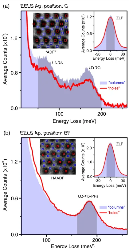
In Fig.2(a)we explore the sensitivity of the vibrational-loss spectrum to probe position for the aperture at position C (almost equivalent to position A but displaced by 61 mrad), as the probe is scanned across an area of the hexagonal boron nitride flake oriented in a [0001] zone axis. In this orientation of theAA’stacked hexagonal BN flake, atomic columns consisting of alternating B and N atoms through the thickness of the sample are arranged in a honeycomb pattern [24,25]. The flake thickness was
HAADF inner angle HAADF inner angle
BF
50 mrad
(b)
BF: Counts (x10
s
)
3-1
A,B: Counts (x10
s
)
2-1
1.0 2.0
0.0 2.0
4.0
0.0
Energy Loss (meV)
0 100 200
-100
BF
B A
LO-TO LA-TA
LO-TO-PPs ZLP
hBN [0001]
(a)
A
B
c
[image:2.612.333.544.46.396.2]estimated to be 153nm, corresponding to between 40 and 50 BN layers. The result labeled columns is obtained by averaging spectra recorded when the probe is on the columns (blue squares in the inset on the left-hand side) and that labeled holes when the probe is between the columns (red squares). There is a clear dependence of the signal on probe position, with the intensity of the phonon sector of the spectrum increasing noticeably when the probe is on the columns as the EELS aperture is positioned off axis in position C.
When the EELS aperture is on axis in the BF position, Fig. 2(b), the LA-TA peak seen in Fig. 2(b)is no longer
evident. This is consistent with calculations that suggest theLO-TO-PPs peaks at approximately 170 meV are the dominant contribution to spectra recorded in these exper-imental conditions[11,12]. Furthermore, the sensitivity to probe position of the spectrum in theLO-TO-PPs region is now strongly damped. A further feature in Fig.2(b)is an increase in signal within the tail of the zero-loss peak, below about 100 meV, when the probe is in the holes between the columns compared to when it is positioned on the columns. We will elaborate on this in the discussion of Fig.4.
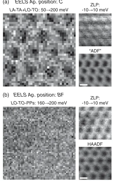
In view of the clear dependence of the spectrum on probe position observed in Fig.2(a), it makes sense to form EELS maps by integrating the signal over the energy-loss sectors indicated in the spectra. Shown in Fig. 3(a), where the detector is in positionC, are the maps from the quasielastic zero-loss peak, −10→10meV, and the phonon sector, with the range 50→200meV encompassing all the phonon modes expected to dominate the spectrum intensity in this geometry [12]. These can be compared with the signal simultaneously recorded by the HAADF detector, which due to the diffraction pattern shift is not symmet-rically placed, hence the nomenclature “ADF.” Note that separate maps of the optical or of the acoustic peaks alone using narrower integration windows show the same overall contrast as the50→200meV map, but with poorer signal to noise (see the additional data provided in [22]). The contrast of the phonon sector map mirrors that of the ADF image, significantly different from that of the ZLP map— see also[22], and is consistent with the map in Fig.3(a) being dominated by inelastic phonon scattering.
Similar results are shown in Fig.3(b)for the detector in position BF, but the integration of the phonon sector covers a different range 160→200meV, that which includes the optical phonon energy losses known to dominate the spectrum in the on-axis geometry[12]. This map shows the lack of contrast consistent with the discussion of Fig.2(b). Clearly, if phonon excitation events with suitably large momentum transfers are used to form the image then atomic resolution mapping is possible, something which is self-evident if one accepts that a conventional HAADF detector is effectively integrating over the phonon spectrum for a suitably large range ofq values to yield an atomic resolution image. Here, we have shown that this is also possible for a range of somewhat smallerqvalues for the detector positionC.
The interpretation of the experimental results is further validated in Fig.4(a)by simulations for a 15 nm thick slab ofAA’-stacked hexagonal boron nitride, carried out using the QEP model[19], when the convergent-beam diffraction (CBED) pattern expected on the detector is effectively shifted so that positionCcoincides with the detector in the forward direction (top right panel)—i.e., by a magnitude of 61 mrad in the direction shown. The left panel shows the spectrum map for phonons scattered into the 22 mrad
A
v
erage Counts (x10
)
3
0.6 1.2
0.0
100
1.0 2.0
0.0
Energy Loss (meV)
A
verage Counts (x10
)
5
-30 30
Energy Loss (meV) 0
-30 30
Energy Loss (meV) 0
0.8 1.6
0.0
A
verage Counts (x10
)
2
100 200
Energy Loss (meV)
(b) (a)
A
verage Counts (x10
)
3
0.6 1.2
0.0
EELS Ap. position: BF EELS Ap. position: C
200
“columns”
“holes”
“ADF”
HAADF
“columns”
“holes” LO-TO LA-TA
LO-TO-PPs
[image:3.612.69.279.42.445.2]ZLP ZLP
detector. These results are calculated using an Einstein model—to a very good approximation, the same as the integrated spectrum in a correlated model[26]. Last, we have the signal into the HAADF detector, again denoted ADF.
Figure4(b)is the same as Fig.4(a)but for no deflection of the diffraction pattern. Note that in this case the contrast of the spectrum map for scattering into the 22 mrad detector is reduced by a factor of ≈3, defined in terms of the maximum and minimum intensity by ðImax−IminÞ=
ðImaxþIminÞ. Each of Figs. 4(a) and 4(b) is plotted on its own gray scale for visibility, so that the contrast in Fig. 4(b) is “stretched” relative to that in Fig. 4(a) and artificially appears stronger than it is in absolute terms. The simulations in Fig.4were done taking into account the high resolution (impact) scattering. The slowly varying background due to the delocalized dipole scattering [18,27], important for small momentum transfersq, further diminishes contrast, consistent with the experimental results shown in the left panel of Fig.3(b).
Simulations exploring the angular dependence of the contributions to the contrast of the spectrum map in Fig. 4(b) are shown in [22]. The contrast reversal for 0≲15mrad is consistent with the observation, made when discussing Fig. 2(b), that there is more signal for energy
losses≲100meV when the probe is in the holes between the columns; smaller momentum transfers are correlated with smaller energy losses[26]. The contributions from the (larger area) annular region from approximately 15 to 22 mrad (and which correlates with larger energy losses), where there is more signal on the columns, dominates the contrast to give the result shown in the left panel of Fig.4(b). The slight minima on atomic sites in Fig.4(b)are attributable to more scattering to largerqwhen the probe couples to a column.
In conclusion, we have shown that there are atomic-scale variations in the vibrational-loss spectrum from a thin flake of hexagonal boron nitride as an atomic-sized probe is scanned across the specimen. In particular, spectral map-ping of atomic structure using the phonon sector of the energy-loss spectrum is demonstrated for an off-axis collection geometry, a setup which also suppresses the contribution due to dipole scattering. Possible future
"ADF"
HAADF CBED
CBED (a) EELS Ap. position: C
0-22 mrad
0-22 mrad (b) EELS Ap. position: BF
Contrast: 0.52
[image:4.612.78.269.48.352.2]Contrast: 0.17
FIG. 4. (a) Simulations of the CBED pattern tilted to effec-tively put the detector, in the forward direction, in positionC; of the spectrum map into the 22 mrad detector; and of the image into the ADF detector. (b) The same as (a) but the detector is in the BF position. The contrast is defined in terms of the maximum and minimum intensity by ðImax−IminÞ=
ðImaxþIminÞ. Scale bars: 2 Å.
(a)
ZLP:
LA-TA LO-TO+ : 50 200 meV -10 10 meV
“ADF”
ZLP:
LO-TO-PPs: 160 200 meV -10 10 meV
HAADF
(b) EELS Ap. position: BF EELS Ap. position: C
[image:4.612.338.535.51.384.2]applications of this technique include mapping of localized, defect-induced, finiteqvibrational modes as well as similar local modifications of the vibrational response of materials. Additionally, these results support the quantum excitation of phonons model and confirm that the standard technique of Z-contrast imaging is based on the inelastic scattering associated with phonon excitations, not consistent with the frozen phonon model which assumes elastic scattering from different configurations of the atoms in the specimen.
This research was supported under the Discovery Projects funding scheme (Project No. DP140102538) of the Australian Research Council and by the Alexander von Humboldt Foundation. L. J. A. thanks Dr. Hamish Brown and Dr. Scott Findlay for helpful discussions. SuperSTEM is the U.K. Engineering and Physical Sciences Research Council (EPSRC) National Research Facility for Advanced Electron Microscopy.
*
[email protected] †[email protected] ‡[email protected]
[1] O. L. Krivanek, T. C. Lovejoy, N. Dellby, T. Aoki, R. W. Carpenter, P. Rez, E. Soignard, J. Zhu, P. E. Batson, M. J. Lagos, R. F. Egerton, and P. A. Crozier, Nature (London)
514, 209 (2014).
[2] T. Miyata, M. Fukuyama, A. Hibara, E. Okunishi, M. Mukai, and T. Mizoguchi,Microscopy63, 377 (2014). [3] T. C. Lovejoy, G. C. Corbin, N. Dellby, M. V. Hoffman, and
O. L. Krivanek,Microsc. Microanal.24, 446 (2018). [4] O. Krivanek, N. Dellby, T. Lovejoy, N. Bacon, G. Corbin,
P. Hrncirik, Z. S. Szilagyi, T. Aoki, R. W. Carpenter, and P. A. Crozieret al.,Microsc. Microanal.20, 66 (2014). [5] P. A. Crozier, J. Zhu, T. Aoki, P. Rez, W. J. Bowman, R. W.
Carpenter, O. L. Krivanek, N. Dellby, T. C. Lovejoy, and R. F. Egerton,Microsc. Microanal.20, 72 (2014). [6] R. F. Egerton,Microsc. Microanal.20, 658 (2014). [7] R. Egoavil, N. Gauquelin, G. T. Martinez, S. Van Aert, G. Van
Tendeloo, and J. Verbeeck,Ultramicroscopy147, 1 (2014). [8] P. A. Crozier, T. Aoki, and Q. Liu,Ultramicroscopy169, 30
(2016).
[9] M. J. Lagos, A. Trügler, U. Hohenester, and P. E. Batson, Nature (London)543, 529 (2017).
[10] J. C. Idrobo, A. R. Lupini, T. Feng, R. R. Unocic, F. S. Walden, D. S. Gardiner, T. C. Lovejoy, N. Dellby, S. T. Pantelides, and O. L. Krivanek, Phys. Rev. Lett. 120, 095901 (2018).
[11] F. S. Hage, R. J. Nicholls, J. R. Yates, D. G. McCulloch, T. C. Lovejoy, N. Dellby, O. L. Krivanek, K. Refson, and Q. M. Ramasse,Sci. Adv.4, eaar7495 (2018). [12] R. J. Nicholls, F. S. Hage, D. G. McCulloch, Q. M. Ramasse,
K. Refson, and J. R. Yates,arXiv:1804.10475. [13] P. Rez,Ultramicroscopy52, 260 (1993). [14] C. Dwyer,Phys. Rev. B89, 054103 (2014). [15] P. Rez,Microsc. Microanal.20, 671 (2014).
[16] N. R. Lugg, B. D. Forbes, S. D. Findlay, and L. J. Allen, Phys. Rev. B91, 144108 (2015).
[17] C. Dwyer, T. Aoki, P. Rez, S. L. Y. Chang, T. C. Lovejoy, and O. L. Krivanek, Phys. Rev. Lett. 117, 256101 (2016).
[18] C. Dwyer,Phys. Rev. B96, 224102 (2017).
[19] B. D. Forbes, A. V. Martin, S. D. Findlay, A. J. D’Alfonso, and L. J. Allen, Phys. Rev. B82, 104103 (2010). [20] R. F. Loane, P. Xu, and J. Silcox,Acta Crystallogr. Sect. A
47, 267 (1991).
[21] E. J. Kirkland,Advanced Computing in Electron Micros-copy (Springer Science & Business Media, New York, 2010).
[22] See Supplemental Material at http://link.aps.org/
supplemental/10.1103/PhysRevLett.122.016103 for more
experimental parameters; Fig. S1, experimental off-axis spectrum maps of the LA-TA and LO-TO phonon-loss peaks, and Fig. S2, annular contributions to Fig. 4(b) over the ranges 0–15 mrad and 15–22 mrad.
[23] A. A. Govyadinov, A. Konečná, A. Chuvilin, S. V´elez, I. Dolado, A. Y. Nikitin, S. Lopatin, F. Casanova, L. E. Hueso, J. Aizpurua, and R. Hillenbrand, Nat. Commun. 8, 95 (2017).
[24] A. Shmeliov, J. S. Kim, K. B. Borisenko, P. Wang, E. Okunishi, M. Shannon, A. I. Kirkland, P. D. Nellist, and V. Nicolosi,Nanoscale5, 2290 (2013).
[25] G. Constantinescu, A. Kuc, and T. Heine,Phys. Rev. Lett.
111, 036104 (2013).
[26] B. D. Forbes and L. J. Allen, Phys. Rev. B 94, 014110 (2016).