Int. J. Electrochem. Sci., 8 (2013) 6988 - 6996
International Journal of
ELECTROCHEMICAL
SCIENCE
www.electrochemsci.orgFabrication and Characterization of an
n
-CdO/
p
-Si Solar Cell
by Thermal Evaporation in a Vacuum
M. Zaien1,2,*, N. M. Ahmed1, and Z.Hassan1
1
Nano-Optoelectronics Research and Technology Laboratory, School of Physics, Universiti Sains Malaysia, 11800 USM, Penang, Malaysia
2
Department of Physics, College of Education for Pure Sciences, University of Anbar, Iraq *
E-mail: mustafa1973_zzz@yahoo.com
Received: 7 February 2013 / Accepted: 5 April 2013 / Published: 1 May 2013
A CdO/Si solar cell was fabricated via deposition of a CdO thin film on p-type silicon substrate at room temperature by thermal evaporation technique for CdO powder in a vacuum (2.2 105
mbar). The synthesized thin film has a thickness of approximately 346 nm. Scanning electron microscopy revealed that the thin film had a good quality structure. X-ray diffraction and energy dispersive X-ray analysis were used to characterize the structural properties of the solar cell. The CdO thin film had a grain size of 34 nm. The solar cell yielded a minimum effective reflectance that exhibited excellent light-trapping at wavelengths ranging from 400 nm to 1000 nm. Photoluminescence spectroscopy was conducted to investigate the optical properties. The direct band gap energy of the CdO thin film was 2.46 eV. The photovoltaic properties of the CdO/Si solar cell were examined under 100 mW/cm2 solar radiation. The cell had an open circuit voltage (Voc) of 460 mV, a short-circuit current density (Jsc) of 18.8 mA/cm2, a fill factor (FF) of 0.685, and a conversion efficiency (η) of 5.92%.
Keywords: Cadmium oxide ; Thin film ; Thermal evaporation in vacuum ; Solar cell.
1. INTRODUCTION
2. MATERIALS AND METHODOLOGY
A CdO/Si solar cell was fabricated using the thermal evaporation technique in a vacuum system of 2.2 10-5 mbar, with a thin film thickness of approximately 346 nm. This method was selected because of its lower cost and simplicity. The RCA (Radio Corporation of America) process was used to remove the oxide layer from a p-type Si wafer (1 cm × 1 cm × 283 μm) with a (111) orientation and a resistivity of 0.75 Ω cm. The Alcatel-101 evaporator system, equipped with a common diffusion and rotary pump, was used to evacuate the high vacuum chamber. The Si substrate was loaded onto the holder at the top of the vacuum chamber, whereas a tungsten boat was used to hold molten CdO for evaporation. The CdO powder (purity, 99.99%; Aldrich) as the source of CdO was loaded onto a tungsten crucible. Prior to CdO deposition, the tungsten boat was cleaned with alcohol to remove any contamination and dried using nitrogen gas. The vacuum chamber was evacuated to 2.2 10-5
mbar before the source was heated. The tungsten boat was then heated using 60 Amp of direct current for 10 sec to melt the CdO. The current was increased slowly to 160 Amp until all CdO evaporated. The substrate was then removed after waiting a few minutes for the chamber to cool down.
[image:2.596.171.426.504.703.2]
Figure 2. Schematic illustration of the (n-CdO/p-Si) solar cell.
Silver evaporation was used in front of the sample (n-CdO) to form metallization grid pattern as shown in Fig. 1, whereas aluminum evaporation was used at the back (p-Si) to form a reflector contact via thermal evaporation in a vacuum (Edwards Auto 306). The schematic illustration of the (n-CdO/p-Si) solar cell is shown in Fig. 2. Annealing was achieved at 400 °C for 20 min to ensure optimal contact.
X-ray diffraction (XRD) measurements were carried out using a high-resolution X-ray diffractometer system (X’Pert PRO MRD PW3040, PANalytical) to determine the CdO crystallite structure. Scanning electron microscopy (SEM) and energy dispersive X-ray (EDX) analysis (JSM-6460 LV, Japan) were conducted to determine the surface morphology and composition of the CdO/Si, respectively.The photoluminescence (PL) study was carried out via a spectroscopy system (HR 800UV, Jobin Yvon, USA) at room temperature using He-Cd laser (λ = 325 nm). CdO thin film thickness and optical reflectance of the CdO/Si were measured using an optical reflectometer (Filmetrics, F20, USA). Topography of the thin film was studied using atomic force microscopy (AFM) (Dimension edge, Bruker) with tapping operation mode. Current density-Voltage (J–V) measurements were performed in forward bias with a computer-controlled Keithley 2400 Source Meter under 100 mW/cm2 illumination from a solar simulator. A 100 W xenon lamp served as the light source, and the light intensity was calibrated using a standard silicon solar cell.
3. RESULTS AND DISCUSSION
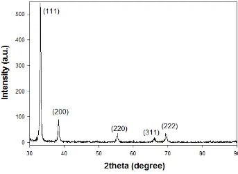
Fig. 3 shows the XRD patterns of the CdO thin film on Si substrate. The diffraction peaks observed at diffraction 2θ angles of 33o
O ZZ
C
%
(2)
Where C represents the lattice constant of the CdO thin film estimated from XRD data and CO
[image:4.596.124.467.356.607.2]is the standard lattice constant for the unstrained CdO [19]. The negative value of the strain (− 0.068%) revealed the compressive strain of the CdO thin film. This low value of compressive strain suggests that the synthesized CdO thin film have high-quality crystal geometry.
Figure 3. XRD spectrum of the CdO thin film on silicon substrate.
concentrations of these elements are indicated by the peaks, showing clearly that the elements corresponding to the peaks comprise the CdO/Si without impurities.
Figure 4. SEM image and EDX analysis of the CdO/Si.
Fig. 5 shows an SEM cross-sectional image of the CdO/Si. The CdO thin film was distinguished due to its different structure with Si substrate and has formed a uniform surface over the entire substrate. The figure also reveals the thickness of the CdO thin film was 346 nm.
Figure 5. SEM cross-sectional image of the CdO/Si.
[image:5.596.102.496.132.334.2] [image:5.596.170.421.468.638.2]Figure 6. Photoluminescence spectroscopy of the CdO/Si.
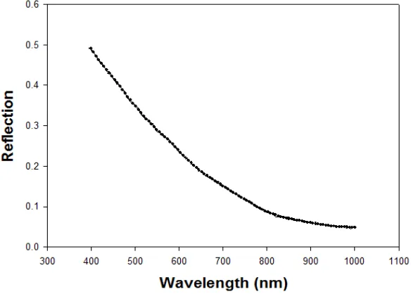
AFM was used to characterize the topography (2D, 3D) of the CdO thin film, as shown in Fig. 7. The mean surface roughness was measured to be 65.73 nm. Therefore, the high degree of roughness of the CdO thin film reduces light reflection, but increases light absorption in the visible region of the solar spectrum in solar cells.
Figure 7. Atomic Force Microscope (AFM) (3D, 2D) of the CdO/Si.
[image:6.596.144.450.69.303.2] [image:6.596.111.491.454.637.2]
Figure 8. Reflection spectra of the CdO/Si.
Fig. 9 shows the J–V characteristics of the solar cell under a 100 mW/cm2 illumination condition.
Figure 9. Current density-Voltage curves of the (n-CdO/p-Si) solar cell.
In the present study, the CdO/Si solar cell has an open-circuit voltage (Voc) of 460 mV, a short-circuit current density (Jsc) of 18.8 mA/cm2, a maximum voltage (Vmax) of 359 mV, and a maximum current (Jmax) of 16.5 mA/cm2. The fill factor (FF) was calculated as follows [20,16]:
OC
SC V
J V J FF
max max
[image:7.596.125.477.401.615.2]4. CONCLUSION
A CdO thin film was successfully deposited on a p-Si substrate to yield a solar cell via thermal evaporation in a vacuum. The XRD pattern showed that the thin film was polycrystalline in nature with a cubic structure and that the prepared film has a (111) preferred orientation. SEM results showed that the thin film exhibited a uniform surface morphology over the entire substrate and has a good quality structure. The direct band gap energy of the CdO thin film was 2.46 eV. The minimum effective reflectance was obtained from the deposition of the n-CdO on the p-Si substrate, evidently reducing light reflection and increasing light-trapping at 400 mm to 1000 nm wavelengths due to the high degree of roughness and large thickness of the CdO thin film. Moreover, the solar cell conversion efficiency (n-CdO/p-Si) was 5.92% under a 100 mW/cm2 illumination condition using thermal evaporation in a vacuum.
ACKNOWLEDGEMENT
The authors gratefully acknowledge the support of the School of Physics in Universiti Sains Malaysia.
References
1. L. M. Su , N. Grote and F. Schmitt, Electron.Lett., 20 (1984 ) 716-717.
2. Z. Zhao, D. L. Morel and C. S. Ferekides, Thin Solid Films, 413 (2002) 203-211. 3. Y. Hames and S. E. San, Solar Energy, 77 (2004) 291-294.
4. K. Senthil, Y. Tak, M. Soel and K. Yong, J. Nanoscale Res Lett., 4 (2009) 1329-1334.
5. K. Gurumurugan, D. Mangalaraj and Sa. K. Narayandass, J. Cryst. Growth, 147 (1995) 355-360. 6. M. Ristić, S. Popović and S. Musić, Mater. Lett., 58 (2004 ) 2494-2499.
7. S. Reddy, B. E. Kumara Swamy, Umesh Chandra, B. S. Sherigara and H. Jayadevappa, Int. J.Electrochem. Sci., 5 (2010) 10-17.
8. K. T. Ramakrishna Reddy, G. M. Shanthini, D. Johnston and R. W. Miles, Thin Solid Films, 427 (2003) 397-400.
9. M. Ortega, G. Santane and A. Morales-Acevedo, superficies y Vacio, 9 (1999) 294-295. 10.F. A. Benko and F. P. Koffyberg, Solid State Commun., 57 (1986) 901-903.
11.R. J. Deokate, S. M. Pawar, A. V. Moholkar, V. S. Sawant, C. A. Pawar, C. H. Bhosale and K. Y. Rajpure, Appl. Surf. Sci., 254 (2008) 2187-2195.
13.D. S. Dhawale, A. M. More, S. S. Latthe, K. Y. Rajpure and C. D. Lokhande, Applied Surface Science, 254 (2008) 3269-3273.
14.P. K. Ghosh, S. Das, S. Kundoo and K. K. Chattopadhyay, J.Sol-Gel Science and Technology, 34 (2005) 173-179.
15.Tz-Jun Kuo and Michael H. Huang, J. Phys.Chem. B, 110 (2006) 13717-13721.
16.M. Zaien, N. M. Ahmed and Z. Hassan, Superlattices and Microstructures, 52 (2012) 800-806. 17.M. Zaien, N. M. Ahmed and Z. Hassan, Advanced Materials Research, 620 (2013) 241-245. 18.C.-Y. Tsay, K.-S. Fan, S.-H. Chen and C.-H. Tsai, J. Alloys Compd., 495 (2010) 126-130. 19.C. Dantus, R. S. Rusu and G. I. Rusu, Superlattices and Microstructures, 50 (2011) 303-310. 20.B. Alfa, M. T. Tsepav, R. L. Njinga and I. Abdulrauf, Applied Physics Research, 4 ( 2012) 48-56.