Int. J. Electrochem. Sci., 8 (2013) 7724 - 7733
International Journal of
ELECTROCHEMICAL
SCIENCE
www.electrochemsci.org
Synthesis and Characterization of ZnO Flower-Like Multisheets
Grown on Metal Buffer Layer
A. Kamalianfar1,3,5*, S.A.Halim1,2*, Mahmoud Goodarz Naseri1,5 , M. Navasery1, Fasih Ud Din1, J. A. M. Zahedi4, K.P.Lim1, E.B.Saion1 and C.K.Chen1, A.Lavari Monfared 6
1
Department of Physics, Faculty of Science, University Putra Malaysia, 43400 UPM Serdang, Selangor, Malaysia
2
Institute of Advanced Materials, University Putra Malaysia, 43400 UPM Serdang, Selangor, Malaysia
3
Department of Physics, Jahrom University, Jahrom, Iran
4
Department of Physics, Karaj Branch, Islamic Azad University, Karaj, Iran
5
Department of Physics, Faculty of Science, Malayer University, Malayer, Iran
6
Department of Physics, Faculty of Science, Farhangian University, Iran
*
E-mail: [email protected] , [email protected]
Received: 24 January 2013 / Accepted: 3 May 2013 / Published: 1 June 2013
ZnO flower-like multisheets were synthesized on Si (1 1 1) and corning glass substrates with Cu and Au-Cu alloy buffer layers via vapor phase transport (VPT) method. The structures and morphologies of the products were investigated using X-ray diffraction (XRD) and field emission scanning electron microscopy (FESEM). The flowers have several parallel petal-like nanosheets that are perpendicular to the main axis. The metal buffer layer affects the growth rates and initial nucleation of ZnO structures, resulting in different numbers and shapes of petals. The optical properties were studied with photoluminescence (PL) and Raman spectroscopy. The intensity of the visible emission peak for Cu coated silicon was the lowest, which may indicate that the surface of defects being covered with Cu atoms. The presence of the E1(LO) and A1(LO) phonon peaks in the Raman spectra reveal the status of
c-axis and the surface of the samples. In addition, the growth mechanism of the ZnO flower-like multisheet structure was investigated based on the FESEM images for different growth times.
Keywords: ZnO nano/microstructure, Flower-like, ZnO multisheet, superlattice.
1. INTRODUCTION
method, a number of morphologies can be produced [1]. During the past decades, a significant step after the growth of single component nanostructures is the synthesis of hetero-structure nanocrystals of materials. The study of metal interfaces in metal-semiconductor hetero-structure nanocrystals systems has been of great interest to improve the optical properties including luminescence intensity and enhance the efficiency of light-emitting materials [2,3]. Additional, the interaction between the components can produce new physical properties which may be of great use in electronic and optoelectronic devices.
A versatile semiconductor material, Wurtzite ZnO has a wide direct band gap (Eg=3.37 eV) and high value exciton binding energy (~ 60 meV), making it a promising candidate for optoelectronic devices, UV lasers, and sensors [4,5,6]. In addition to one dimensional ZnO structures, some novel nano- and micro-scale morphologies, such as sheets, plates, disks and flowers, in two or three dimensions are of interest for their high surface to volume ratio, nanometer scale thickness, excellent permeation, and distinct optical and photocatalytic activities for applications such as sensing [7,8,9].
In other side, some metals transform to their oxide phase during experiment process due to the high temperature condition. Therefore, the integration of wurzite ZnO with metal oxide provides a hetero-junction with the unique ferroelectric, ferromagnetic and sensing properties which has strong potential for applications in Humidity Sensor [10], and gas sensors [11].
ZnO structures have been synthesized with various methods, such as chemical vapour deposition [12], vapor-phase oxidation of metallic Zn powders [13], and pulsed laser deposition [14]. Vapor phase transport is a simple and cost-effective approach frequently used to grow micro and nanostructures on a relatively large scale.
Herein, we study the effect of Cu and Au-Cu alloy buffer layer on morphological and optical properties of flower-like ZnO structures on silicon and corning glass substrates via the vapor phase transport method. All the substrates were placed close to each others to maintain the same growth conditions. As a point of reference, clean silicon and glass were also chosen. The products were characterized and the proposed growth mechanism explained.
2. EXPERIMENTAL
electric tube. The sample was heated at a rate of 20˚C/min. When the temperature of the furnace reached to 700˚C, nitrogen as carrier gas was supplied to the furnace tube at a constant rate of 70 sccm. The temperature and gas flow rate were kept constant during the growth process for 50 minutes, while the temperature of the source was 950 °C. Under these conditions, the substrate temperatures were estimated to be approximately 650 °C. Finally, the electric furnace was cooled to room temperature.
The phase of the ZnO microstructures was determined using X-ray diffraction, performed on a XPERT PRO PANALYTIAL (pw 3040 MPD) XRD diffraction spectrometer. Field emission scanning electron microscopy (FESEM, JSM 6700) was used to observe the morphology of the samples. The room temperature PL and Raman spectrum of the samples were recorded with a fluorescence spectrometer (LS 55) using a Xe lamp at room temperature with an excitation wavelength of 320nm and Raman spectrometer (Renishaw inVia with λ=514 nm laser excitation), respectively.
3. RESULTS AND DISCUSSION
3.1. Structural and morphological properties
[image:3.596.126.468.359.727.2]
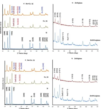
Fig.1 shows the XRD patterns of ZnO as-grown flower-like multisheet ZnO on different substrates. Fig .1(a) presents a comparison of the XRD patterns for ZnO flowers grown on Cu/Si and Au-Cu/Si substrates with a clean silicon substrate. The ZnO diffraction peaks can be indexed to the hexagonal wurtzite structure with lattice constants of a= 3.2490 Å and c=5.2050 Å (PDF Card No. 00-005-0664).
The intensity of the ZnO diffraction peaks grown on the Si was greater than those with buffer layers. In addition, the diffraction peaks of the flowers grown on the metal buffer layers were broader than those of the clean silicon substrate. This broadening can be attributed to a distribution of strain in the flowers samples due to different degrees of bending [15]. The relative intensity of the XRD diffraction peaks in the samples with metal buffer layers are attributed not only to the ZnO structure, but also to the buffer layers (i.e from Cu and its oxide CuO). It can be suggested that the combination of the metal buffer layers with Zn and O forms a new phase of zinc-metal.
Therefore, the peak at 43.3 and a low intensity peak at approximately 39 can be indexed to Cu (1 1 1) (PDF Card 01-085-1326) and CuO (1 1 1) (PDF Card 00-0011-1117) due to oxidation of copper at temperatures above 350 C. In case of Au+Cu/Si, three extra peaks at 39.1 , 44.5 and 64 attributed to the gold were observed in the pattern.
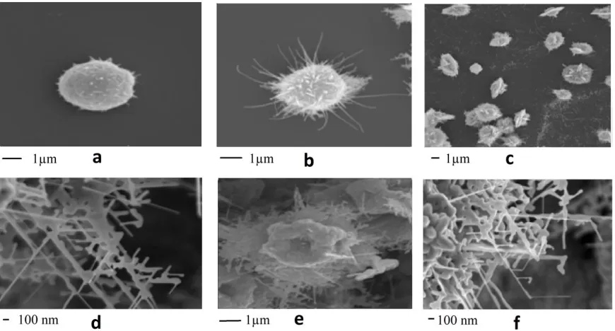
Figure 2. FESEM images of ZnO flower-like multisheets on : a) a clean Si covered with multisheets flowers b) clean Si c) Cu/Si d) Au+Cu/Si e) Cu/glass f) clean glass
[image:4.596.65.527.357.655.2]
This indicates that the copper and glass alloy prepared a new surface condition to absorb Zn and assist the formation of a crystalline structure.
Fig .2 shows the morphological features of the as-prepared ZnO samples. The surfaces of the substrates were densely covered with the ZnO flower-like multisheets (Fig .2(a)). The high magnification images provide a closer view of typical flower morphology of the samples (Fig .2(b-e)). Each flower consists of several parallel nanosheets that are perpendicular to the main axis in the form of petal-like film.
Overall, although the flowers have various shapes, the diameter of the petals became smaller starting from the base of the lowest node and working upwards. The change in the diameter of the nanosheets or petals during the growth process can be assigned to variation in the growth velocity. ZnO is a polar surface due to Zn+2 and O-2 ions. For ZnO, the speed of growth for the {001} direction is significantly faster than {100} and {210}, because the growth speed is crystallographic-direction-dependent. The depletion of building blocks in combination with the polar features enables a change in the growth speed. Changing in the growth relation may cause a prismatic growth of the nanosheets on the parallel planes. The various morphologies produce under the same conditions reveal the effect of the substrate on the initial nucleation. Fig .2(b) shows a typical flower grown on the clean silicon substrate. The flower has a number of symmetric petal-like nanosheets. The petals in each plane are connected to the center and the planes are nearly parallel to each other. The average height of a typical flower is several micrometers. The average dimensions of these interwoven petals were estimated to be in the range of 200–300 nm, with thickness of 100–150 nm. A typical flower grown on Cu/Si substrate is shown in Fig .2(c). The flower has only two or three petals. The upper sheet consists of a hemisphere with ZnO nanowires extending out from it.
Fig. 2(d) shows a generic flower grown on the Au-Cu alloy coated silicon substrate. The main feature of the flowers is a hole on the size range of 1-2 micrometers on the surface of most flowers. The holes on the surface structural probably formed during the ripening or initial nucleation of the flowers (see also Fig. 3(e)). The morphology of the as-grown ZnO on amorphous corning glass is different. Interference in formation of multisheet clearly can be observed in Fig. 2(f). The Cu coated glass substrate has an organized morphology as shown in Fig. 2(e). The obtained morphology is similar to a rose flower. Although the boundaries of the sheets are not very smooth, the average diameter of the petals is on the range of 3-4 micrometers. Comparison between Fig. 2(c) and Fig. 2(e), indicates that the Cu buffer layer has a significant effect on the initial nucleation of the Zn on the corning glass. Due to the fixed external conditions such as temperature for all the samples, formation of different flower shapes can be attributed to the internal parameters such as buffer layer. It means that the formation of ZnO structure directly related to the most stable adsorption locations. In result, the Surface geometry and adsorption sites (e.g hcp or fcc) of buffer layers are significant parameters for initial nucleation of Zn on the surfaces.
3.2. Mechanism of growth
complex structures such as ZnO architectures and hierarchical nanostructures and also no Cu or Au signal was detected by EDX analysis (not shown here). Thus, the vapor-solid (VS) process is the most likely process to explain the formation of complex structures.
The proposal process of the growth is shown in Fig .3. A multisheet consists of several 2D nanosheets. In the VPT method, ZnO powders will be reduced to Zn or ZnOx (x<1) in vapor phase, which are transported toward the lower temperature zone of the furnace, and after absorption by the substrate, they form a droplet.
Figure 3. (a-e) Process of formation of ZnO flower-like multisheets f) dendrites in different planes.
The wet surface has a higher sticking coefficient and is a preferred absorption site [16], resulting in the formation of microstructured of Zn or ZnO (after combination with oxygen), as shown in Fig. 3(a). Under ambient conditions and due to the large iconicity of the bands between atoms of zinc and oxygen, the vicinity of the Zn+2 and O-2 results ZnO nanowires extend out from Zn particle (Fig. 3(b)). In the solidification process of metal alloys [17], a regular crystal growth morphology is dendrite shape (Fig. 3(d)). The different branches of the dendrites can change shape into 2D sheet-like structure by crystal growth into the space between the dendrite arms on the same plane (Fig. 3(e). Hence, 2D sheet-like appears with a thickness on the same order as, or greater than, the main arm of the dendrite. Finally, this process of branching of the dendrites in different planes leads to the formation of a multisheet (Fig. 3(f)).
4. OPTICAL PROPERTIES
4.1. Raman spectroscopy
[image:6.596.74.509.209.443.2]
Raman features of the samples at room temperature. For the samples on the silicon substrate, a sharp peak at 520 cm-1 corresponds to silicon. As it is expected by coating the silicon substrates with buffer layers, the intensity of the related peaks was reduced. A sharp and dominant mode of E2(high) at 436.5
cm-1 for the silicon substrate without buffer layer and 433 cm-1 for silicon with metal buffer layer were detected. The shift of the E2 mode indicated that the nanowires or nanosheets grown on metal buffer
layers are under more in-plane stress [18]. The E2(high) mode for ZnO on the corning glass is very
weak and broad.
A weak E1(TO) mode at 409 cm-1 was found in the spectra of ZnO grown on the silicon
substrate due to the polycrystalline structure. For ZnO bulk crystal, the frequency of A1(LO) phonon
peak at 574 cm-1 appears when the surface of the sample and c-axis of wurtzite ZnO are parallel, and the presence of E1(LO) phonon peak at 583 cm-1 appears when they are perpendicular [19]. Therefore,
the E1(LO) peak at 583.5 cm-1 in the Si substrate spectrum indicates that the surface of the sample and
c-axis of wurtzite ZnO are perpendicular, however, they are parallel in the case of the Cu/Si and Au-Cu/Si substrates. The peaks at 572.5 and 573.5 cm-1 are shown in Fig .4. This peak also appeared at 572 cm-1 for flowers grown on Cu/glass. The shift in the E1(LO) phonon mode in comparison with
ZnO bulk crystal is probably due to the tensile strain effect, optical phonon confinement, or defects in the multisheet structures. The E1(LO) mode is most likely due to the formation of defects (oxygen
vacancies or zinc interstitials) [20].
[image:7.596.203.399.394.695.2]
From the comparative intensity of E1(LO), it can be understood that the crystal quality of the
sample with the copper buffer layer is better than that of the Au-Cu alloy coated silicon substrate. Other peaks at 332 cm-1 and 380 cm-1 were also observed in the spectrum, and they were assigned to the (E2(h)-E2(l)) (multi phonon), A1(T) modes E1(T) modes, respectively.
4.2. Photoluminescence spectroscopy
[image:8.596.59.537.329.475.2]The recorded PL spectrum of the samples is shown in Fig. 3a and 3b. The PL spectrum of the ZnO grown on silicon substrates consists of a weak UV peak at 375-382 nm and a dominant visible emission manifested as a broad feature in range of 420-550 nm. The UV emission band is attributed to the near band edge emission of ZnO that results from the recombination of free excitons [21]. The broad visible emission is due to the various types of defects [22].
Figure 5. Room temperature PL spectra of the ZnO flower-like multisheets.
of the ZnO grown on it had a broad UV peak centered at 380 nm and the visible emission peak is vanished. This is most likely due to the surface defects being covered by Cu atoms.
5. CONCLUSION
ZnO flower-like multisheets were produced by the vapor phase transport method on silicon and glass substrates with Cu and Au-Cu alloy. The morphology of the grown ZnO on different substrates varied with the introduction of a metal buffer layer. When the amorphous glass substrate was coated with a thin layer of copper, the visible emission peak was suppressed, suggesting that some of the surface defects were covered by Cu atoms indicating a better crystalline structure and enhancing the optical properties. A big hole on the surface of most flowers was observed for ZnO multisheets grown on the Au-Cu alloy coated silicon. The related Pl spectra showed an increase in the surface defects. The experiment reveals the effect of the Surface geometry and adsorption sites (e.g hcp or fcc) of buffer layers are significant parameters for initial nucleation of Zn on the surfaces.
ACKNOWLEDGEMENT
Financial support from Exploratory Research grant (ERGS), ERGS//11/STG/UPM/01/3, is greatly acknowledged.
References
1. X. Y. Kong, Z. L. Wang, Nano Lett. 3 (2003) 1625-1631.
2. J. S. Biteen, D. Pacifici, N. S. Lewis and H. A. Atwater, Nano Lett, 5 (2005) 1768. 3. A. Kamalianfar, S.A.Halim, et al. Chin. Phys. Lett. 29(12) (2012) 128102.
4. H. Kind, H. Yan, B. Messer, M. Law, P. Yang, Adv. Mater. 14 (2002) 158-160. 5. Z. Jing, J. Zhan, Adv. Mater. 20 (2008) 4547-4551.
6. S.M.U. Ali, M. Kashif, Z.H. Ibupoto, M. Fakhar-e-Alam, U. Hashim, and M. Willander,Micro & Nano Letters, 6 (2011) 609-13.
7. Wang N, Lin H, Li J B, Zhang L Z, Li X, Wu J and Li C F, J. Am. Ceram. Soc. 90 (2007) 635-645.. 8. H. T. Ng, J. Li, M. K. Smith, P. Nguyen, A. Cassell, J. Han, M. Meyyappan, Science. 300 (2003)
1249.
9. R. C. Pawar, J. S. Shaikh, S. S. Suryavanshi, P. S. Patil, Curr. Appl. Phys. 12 (2012) 778-783. 10.A. Zainelabdin , G. Amin , S. Zaman , O. Nur , J. Lu , L. Hultman and M. Willander, J. Mater.
Chem. 22 (2012) 11583.
11.Y. W. Zhu, C.H Sow, T. Yu, Q. Zhao, P. Li, Adv Funct Mater. 16 (2006) 2415-2422. 12.Peng Xu, and Huizhao Zhuang,Micro & Nano Letters, 6 (2011) 985-87.
13.Y. Dai, Y. Zhang, Q.K. Li, et al., Chem. Phys. Lett. 358 (2002) 83-86.
14.A.Kamalianfar, S. A. HALIM, et al, J. Optoelectron. Adv. Mater. 15 3-4(2013) 239-243. 15.J. L. Yang, S. J. An, W. I. Park, G. C. Yi, W. Choi, Adv. Mater.16 (2004) 1661-1664. 16.Z. Zhu, T. L. Chen, Y. Gu, J. Warren, R. M. Osgood, Chem Mater. 17 (2005) 4227-4234. 17.Y. Wu, P. Yang, J. Am. Chem. Soc. 123 (2001) 3165-3166.
18.R.D. Doherty, Crystal Growth, 2nd edn., ed. by B.R. Pamplin, Pergamon, Oxford, 1980. 19.J.M. Calleja, M. Cardona, Phys. Rev. B 16 (1977) 3753-3761
21.X. Wang, Q. Li, Z. Liu, J. Zhang, et al., Appl. Phys. Lett. 84 (2004) 4941-4943. 22.Y.C. Kong, D.P. Yu, B. Zhang, et al., Appl. Phys. Lett. 78 (2001) 407-409. 23.R. Dingle, Phys. Rev. Lett. 23 (1969) 579-581.
24.Z.L. Wang, J. Phys. Condens. Matter. 16 (2004) R829.
25.N. Kiomarsipour, R. Shoja Razavi, Superlattic Microst. 52 (2012) 704-710. 26.R. Yousefi, B. Kamaluddin ,Appl. Surf. Sci. 256 (2009) 329-331.