~~
·
apricot
\)
~~
o
apricot
Technical
Portions of this manual contain material reprinted by permission of:
SONY Corporation, Copyright 1982.
TRADEMARKS
MicroScreen is a registered trademark of ACT.
MS is a registered trademark of the Microsoft Corporation.
CP 1M is a registered trademark of Digital Research.
IBM is a registered trademark of International Business Machines.
ACKNOWLEDGEMENTS
ACT wish to acknowledge the invaluable assistance afforded by its consultants in bringing Project Apricot to fruition.
QED Project Design, Clarence House, Newport, Gwent.
CAPA,
Aberdeen House, Highbury Grove, Islington, LondonN2.
Information contained in this document is subject to
change without notice and does not represent a commitment on the part of ACT.
All rights reserved, no use or disclosure without written consent.
Copyright
©
1983 ACT (International) Limited,appendices, as detailed below. This manual is intended for programmers and engineers involved in hardware and software design for Apricot.
l.SYSTEM OVERVIEW
This section provides an overall description of the Apricot computer and is divided into three chapters:
1-1 HARDWARE, describes the hardware of Apricot in
its basic configuration, and forms the introduction to the three elements which constitute the
microcomputer;the System Unit,the Keyboard Unit and the Display Uni t.
1-2 SOFTWARE, provides a brief description of the
operating system and its interface to the associated BIOS. An introduction to the software modules which constitute the BIOS is also provided.
1-3 OPTIONS, forms the introduction to the hardware
options available for the microcomputer, at the time of printing the manual.
2.HARDWARE DETAIL
This section contains a detailed description of all software aspects of the BIOS and is also divided into a number of chapters. The first provides a detailed description of the BIOS as a whole with subsequent chapters detailing the individual hardware drivers.
APPENDICES.
1-1 HARDWARE
CONTENTS ... 1
INTRODUCTION ... ... .... ... ... 1
SYSTEM UNIT ... ... ... .... ... ... ... .... ... 3
KEYBOARD UNIT .... .... ... ... ... ... .... ... ... ... 5
DISPLAY UNIT ... ... ... .... ... ... ... 7
1-2 SOFTWARE CONTENTS ... 1
INTRODUCTION ... ... ... ... ... ... 1
BIOS FEATURES-OVERVIEW OF CAPABILITIES ... ... .... ... ... 2
Foreground and Background Operations ... 2
Multi -sector Reads and Writes ... 3
Tri -buffer ... ... .... .. .. .. .. .. .... .. .. ... .. . . .. .... .. ... ... .... .... 3
Apricot Control Device ... 4
System Configuration Block ... 4
MicroScreen Driver ... 4
Time and Date Clock ... 5
Calculator ... 5
General Hardware Support ... 5
1-3 OPTIONS CONTENTS ... 1
INTRODUCTION ... ... ... ... ... ... 1
FLOPPY DISK OPTIONS .... ... .... ... ... 1
128KBYTERAMEXPANSIONBOARD ... 2
MODEM ... 2
SECTION 2.HARWARE DETAIL
2-1 SYSTEM UNIT
CONTENTS ... 1
INTRODUCTION .... ... ... ... ... ... 1
SYSTEM BOARD ... ... ... ... ... 2
DISK DRIVES ... 3
POWER SUPPLY DETAILS ... 3
General ... 3
DC Supply Distribution ... 4
Fuse Rating ... 4
PHYSICAL DIMENSIONS .... ... ... 5
2-2 SYSTEM BOARD CONTENTS ... 1
INTRODUCTION ... : ... 1
DESCRIPTION ... ... ... ... ... ... ... ... ... 1
Processors ... , ., ., ., . 1
Communications Handling ... 2
Sound Generation ... 3
System Memory ... 3
CRT Controller ... 4
Floppy Disk Controller ... 4
Expansion Slots ... 4
Interrupt Controller ... 4
Timer ... 4
Input/Output Space ... 5
2-3 INTERRUPT CONTROLLER CONTENTS ... 1
INTRODUCTION . ... ... ... ... ... 1
DESCRIPTION ... ... ... .... ... ... 3
General ... 3
Interrupt Sequence ... 4
Interrupt Masking ... 5
PROGRAMMING CONSIDERATIONS ... 5
General ... "'... 5
Initialization Command Words ... 6
2-4 TIMER
CONTENTS ... 1
INTRODUCTION ... ... ... ... ... 1
DESCRIPTION ... ... ... ... ... ... 2
General ... 2
Counter 0 ... 5
Counter 1 and 2 ... 6
Baud Rates ... 8
2-5 CRT CONTROL CONTENTS ... 1
INTRODUCTION ... ... ... .... ... ... 1
DESCRIPTION .... ... ... ... ... ... 2
General ... 2
Mode Selection ... 8
CRTCDETAIL ... , ... 10
General ... 10
Register Description ... 13
Initialising the CR TC ... ... .. .. . ... ... ... .. ... 16
CR TC Connections ... ... 17
SCREEN RAM ... ... ... ... ... ... ... 19
General ... 19
Text Mode ... ... 20
Graphics Mode ... 22
SYSTEM RAM UTILISATION ... ... ... 23
General ... 23
Text Mode ... 24
Graphics Mode ... 25
DISPLAY UNIT CONNECTOR DETAIL ... 26
2-6 FLOPPY DISK INTERFACE CONTENTS ... 1
INTRODUCTION ... ... .... ... ... ... 2
DESCRIPTION ... ... .... ... ... ... 4
General ... 4
Disk Write ... 5
Disk Read ... 5
Disk Formatting ... 6
"-.
FDC DETAIL ... 9
General ... 9
Processor Interface . ... .. .. .. ... ... ... ... 10
Disk Drive Control ... 13
Command Register ... 14
Status Register ... 15
Track Register ... 15
Sector Register ... 15
Data Register ... 16
PROGRAMMING CONSIDERATIONS ... 16
Disk Drive Selection ... 16
Head Loading ... 16
Head Positioning ... 17
Data Transfers ... 21
Formatting Commands ... 26
Force Interrupt Command ... 32
INTERFACE CONNECTION DETAILS ... 33
System Connections ... ... 33
Disk Drive Connections ... 35
TRACKFORMAT ... 37
2-7 SERIAL INTERFACE CONTENTS ... 1
INTRODUCTION ... ... ... .... ... .... ... ... ... .... 1
DESCRIPTION ... ... ... .... ... ... ... 3
General ... 3
SIO Overview ... 4
SIO Architecture ... 6
Processor Interface ... 10
Write Register Definition ... 11
Read Register Definition ... 25
SIO Interrupt Sequence ... 30
KEYBOARD COMMUNICATIONS ... 32
General ... 32
Keyboard Connector Detail ... 33
Channel B Programming Details ... 34
PARALLEL INTERFACE INTERRUPTS ... ... 36
RS232CCOMMUNICATIONS ... 37
General ... 37
RS232C Connector Detail ... ... 38
SIO PIN DETAIL ... 42
System Connections ... 43
Channel A Connections ... 44
Channel B Connections ... 47
2-8 PARALLEL INTERFACE CONTENTS ... 1
INTRODUCTION .. ... .... ... ... ... ... ... 1
DESCRIPTION ... ... .... ... ... 3
General ... 3
Printer Interface ... 4
System Control Interface ... 6
2-9 SOUND GENERATION CONTENTS ... 1
INTRODUCTION .... ... ... ... ... ... 1
DESCRIPTION ... ... ... ... ... ... ... ... ... 2
General ... 2
Tone Generation ... 4
Noise Generation ... 6
2-10 EXPANSION SLOTS CONTENTS ... : ... 1
INTRODUCTION . ... ... ... 1
DESCRIPTION ... 3
Electrical Specification ... 3
Pin Detail .. .. ... . ... .. .. .. .. ... .. .. ... ... 5
Address Allocation ... 10
Expansion Board Layout Detail... 10
2-11 DISK DRIVE CONTENTS ... 1
INTRODUCTION ... ... ... ... ... ... 1
DESCRIPTION ... 2
- General ... 2
Interface Connections ... 3
Disk Drive Mechanism ... 7
Read/Write Head ... 7
Head Load Mechanism ... 7
Sensors and Detectors ... 8
Drive Switch Settings ... 8
Drive Specification ... 9
DISKS ... 10
General ... 10
Disk Precautions ... 11
Disk Insertion/Removal ... 12
Write Protecting ... 12
Disk Format ... 12
2-12 KEYBOARD CONTENTS ... 1
INTRODUCTION ... ... .... ... ... ... .... 1
SERIAL LINK CONTROL AND FORMAT .... ... 2
KEYSWITCH OPERATION ... ... ... ... .... 3
MICROSCREEN OPERATION ... .... ... ... ... 4
CLOCK OPERATION ... 6
MOUSE PORT OPERATION ... 7
KEYBOARD FIRMWARE ... ... ... ... 8
Keyboard to System Unit Character Codes 10 System Unit to Keyboard Character Codes ... 11
2-13 DISPLAY UNIT INTRODUCTION ... ... .... ... ... ... 1
DESCRIPTION .... ... ... ... ... ... ... 1
General ... 1
SECTION
3.S0FTWAR~DETAIL
3-1 PROGRAMMERS GUIDE TO THE BIOS
INTRODUCTION ... ... ... ... ... ... ... 1
BIOS Internal Structure - Memory Map ... 1
VECTORS ... 3
POINTERS ... 3
CHARACTER FONTS 1, 2 and 3 ... 4
SECONDARY CACHE ... 5
PRIMARYCACHE ... 5
SYSINIT ... 5
BIOS CODE ... 5
BIOS CONSTANTS . .... ... ... ... ... ... ... .... 5
GLOBALDATAAREA ... 6
BIOS HEAP AND STACK ... 6
MS-DOS 2.00 ... 6
USERRAM ... 6
3-2 SCREEN DRIVER INTRODUCTION ... ... ... ... .... 1
APPLICATIONS INTEREST .... ... ... 1
Escape Sequence Management Functions ... 1
Environment Flags ... 8
ANSI Escape Sequences ... ... 9
Physical Screen Layout ... 12
Reverse Field Video ... 13
High/Low Intensity ... 13
Underline ... 13
Strikethrough ... 13
Software Reserved ... ... 13
Character Font-cell ... 14
SYSTEMS INTEREST ... 15
CRTC Initialization ... 15
Low-level Display routines ... 15
Cursor management routines ... 15
3-3 MICROSCREEN DRIVER
INTRODUCTION ... ... .... ... ... ... ... ... 1
APPLICATIONS INTEREST ... 1
SYSTEMS INTEREST ... ... ... ... ... 4
3-4 KEYBOARD DRIVER INTRODUCTION ... ... ... ... ... ... 1
APPLICATIONS INTEREST .... ... .... ... ... ... 1
Keyboard Look-up table ... 1
SYSTEMS INTEREST . ... ... ... ... ... 4
Keyboard to Apricot Handler ... ... 4
Key Make Code handler ... ... 5
Key Break Code handler ... 7
Translation of data routines ... 8
Auto Repeat handler ... 8
Non make/break code interpreter ... 8
Queue handlers for data to MS-DOS ... 9
MS-DOS queue ... 9
Local queue ... 9
Keyboard queue ... 10
3-5 CONTROL DEVICE DRIVER INTRODUCTION ... ... ... ... 1
APPLICATIONS INTEREST ... ... .... ... 1
Calling the control device ... 1
Specification of the Apricot Control Device ... 3
Screen Driver ... 3
Keyboard Driver ... 3
MicroScreen Driver ... 5
Serial Port Driver ... 6
Parallel I/O Driver ... 12
Sound Generator ... 14
Floppy Disk Drivers ... 15
Cache/Graphics/IBM configuration ... 16
3-6 DISK INPUT/OUTPUT SYSTEM
INTRODUCTION .. ... ... ... ... ... ... 1
APPLICATIONS INTEREST ... ... ... ... 1
SYSTEMS INTEREST ... 1
Disl< Format ... 2
The Label Sector ... 3
MS-DOS AND BIOS UTILISATION OF THE DISKS ... 4
FAT's 1 and2 ... 4
Directory ... ;... 4
Character Font ... 4
Key board table ... 5
SYSINIT ... 5
BIOS code ... 5
MS-DOS 2.0 ... 5
Configuration data ... 5
3-7 BOOT ROM INTRODUCTION . ... ... ... ... ... ... ... ... 1
APPLICATIONS INTERST ... ... ... ... 1
Software Reset ... 1
Logo display ... 1
3-8 CALCULATOR INTRODUCTION ... ... ... ... 1
APPLICATIONS INTEREST . ... .... ... ... ... .... 1
SYSTEMS INTEREST ... ... .... ... ... .... 2
3-9 SOUND GENERATION INTRODUCTION ... ... ... ... ... ... 1
APPLICATIONS INTEREST ... .... .... ... ... 1
3-10 AUXILIARY DEVICE/SERIAL PORT INTRODUCTION ... ... ... ... ... 1
APPLICATIONS INTEREST ... 1
SYSTEMS INTEREST ... ... ... ... ... 1
3-11 GRAPHICS SYSTEM EXTENSION SYSTEM
INTRODUCTION ... ... ... ... .... ... 1
APPLICATIONS INTEREST ... 1
Graphic System Extension Functions ... ... 1
How to use Graphic Systems Extension ... 1
What is Graphic System Extensions? ... 2
SYSTEMS INTEREST ... .... ... ... 2
GRAPHICS.EXE ... ... ... ... ... ... .... 2
ASSIGN.SYS ... 3
DDACRT.SYS ... 3
ACT GRAPHICS SYSTEM - DDACRT.SYS ... 3
APPENDICES
SYSTEM OVERVIEW
INTRODUCTION . ... ... ... ... ... 1
SYSTEM UNIT ... 3
KEYBOARD UNIT ... ... .... ... ... ... 5
DISPLAY UNIT ... ... ... ... ... ... .... 7
List of Illustrations Figure Apricot Computer ... 1
Apricot Computer block diagram ... 2
INTRODUCTION
The Apricot is the generic name given to a family of 16-bit microcomputers, possessing a diverse range of
hardware facilities to suit the needs and requirements of the user in a wide variety of applications. Each member of the family is produced starting from an Apricot in its basic operational configuration. This is then transformed into a different member of the family by the addition of options, as required. A more detailed treatment of the options is
provided in a subsequent chapter.
All Apricot computers are composed of three separate elements; a System Unit, a Keyboard Unit and a Display
Unit as illustrated on Figure 1.
The System Unit is the area of the computer, which houses the majority of the processing elements, the system memory components and the interface circuitry for
peripheral equipment. The Unit also contains the following items:
(a) At least one micro floppy disk drive. (b) A power supply module.
The Keyboard Unit consists of, a standard layout typewriter keyboard, a calculator keypad, a number of programmable function keys with associated LED
indicators, a set of "fixed" function keys, and a 2 line by 40 character MicroScreen. The Keyboard Unit also contains processing circuitry which provides the interface between the keys and the System Unit.
The standard Display Unit is a high resolution 9 inch monochrome display which fits into a shallow recess on the top of the System Unit. The Display Unit tilts, swivels and slides, enabling the operator to position the screen to obtain the optimum viewing angle. An anti-reflective mesh is incorporated on the screen to minimise the possibility of eye fatigue.
In its basic configuration, the Apricot Computer incorporates the following:
(a) An Intel 8086 16-bit processor.
(b) An Intel 8089 16-bit input/output processor. (c) 256 Kbytes of dynamic RAM.
(d) A single 3.5 inch MicroFloppy disk drive.
(e) A Centronics parallel port for connecting a printer. (f) An RS232C serial interface for data
communica tions.
(g) A port for connecting a "mouse" device. (h) A sound generator to provide audio feedback. (i) Two internal expansion slots to cater for RAM expansion and connecting other optional facilities.
(j) A port for connecting a light pen plus associated
ancillary electronics.
The basic configuration of the microcomputer can be expanded by the addition of two further options, in addition to the optional facilities available via the internal expansion slots. These two further options are as follows:
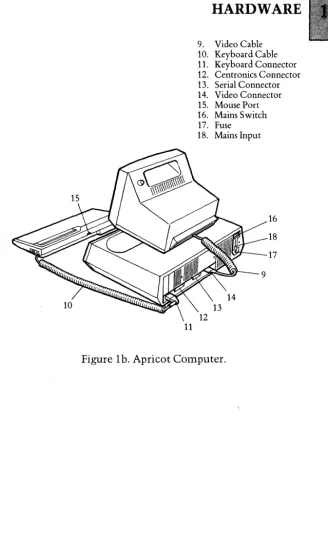
Connections for the printer, data communications equipment and mains input are located at the rear of the System Unit, together with connectors for the Keyboard and Display Units. The expansion slots and the connection for the light pen and associated circuitry are located within the System Unit. The connection for the "mouse" device is located at the rear of the Keyboard Unit.
SYSTEM UNIT
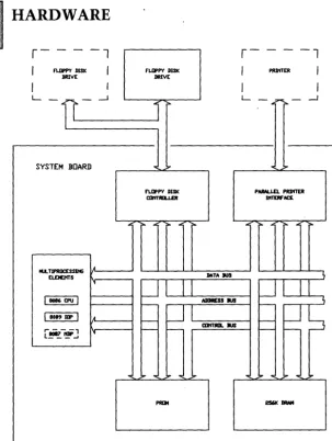
All the processing and control circuitry within the System Unit is contained on a single printed circuit board, designated the System Board, which is 'fitted horizontally inside the System Unit housing. The major elements of the System Board are illustrated on the block diagram, Figure 2a/2b. The System Board incorporates the following items:
(a) The system processing elements. (b) The Boot PROMs.
(c) 256 Kbytes of DRAM. (d) A floppy disk controller. (e) A parallel printer interface.
(f) A dual channel serial interface, one channel for the Keyboard and the other for the RS232C connector. (g) A display controller.
(h) Two expansion slots.
The processing elements on the System Board are
arranged in a multiprocessing configuration which includes two Intel16-bit microprocessors; an 8086 central processing unit (CPU) and an 8089 input/output processor (lOP). The two microprocessors are connected in parallel and share a common bus structure. This configuration is termed (by Intel), a local multiprocessing configuration. The number of microprocessors within the local multiprocessing
configuration is increased to three if the optional lntel8087
numeric data processor (NDP) is fitted.
High speed DMA data transfers, from a selected source (memory or peripheral) toa selected destination (memory or peripheral), are performed by the lOP. The lOP is able to transfer data whilst the central processing unit is engaged in executing tasks which do not require use of the buses.
The 8087 numeric data processor extends the processing capabilities of the Apricot computer, by performing arithmetic and comparison operations on numeric types
which can vary from 16 to 80 bits. It is also able to execute
numerous transcendental functions (e.g.tangent and logari thmic functions).
-The Apricot computer uses 3.5 inch Sony disk drives and employs the IBM system 34 format in the double density mode, with 512 bytes per sector (and 9 sectors per track). The total storage capacity of each disk is 315 Kbytes of formatted data. The floppy disk controller incorporates the necessary capability to control a second floppy disk drive without any modification to the hardware.
The serial interface provides two separate channels; one channel for communication between the System Board and the Keyboard Unit; the second channel for communication between the System Board and data communications equipment. The serial link to the keyboard is a full duplex asynchronous communications channel, which transmits and receives data at a fixed baud rate.
The RS232C channel can be programmed to operate in both asynchronous and synchronous modes, with the programmer having independent control over transmit and receive baud rates. The rates can be generated by either an internal programmable timer or determined by the external data communications equipment. Both byte and bit
oriented synchronous modes are available. These include the byte oriented modes, Monosync and Bisync, and the bit oriented modes, SDLC ana HDLC.
and data buses) plus additional control and timing signals. These include interrupt request lines and control lines for DMA transfers.
Regulated supply voltages, for the System Board,
Keyboard Unit, Monitor Unit, floppy disk drivels) and any optional boards connected to the expansion slots, are supplied from the power supply module located within the System Unit. A switch on the rear of the System Unit switches the mains supply through to the power supply module. An LED in the centre of the Keyboard acts as a power supply present indicator.
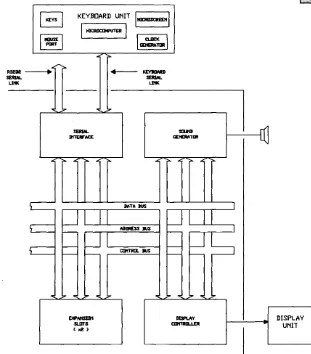
KEYBOARD UNIT
The Keyboard Unit provides the normal interface between the user and the microcomputer. The keys of the Keyboard are divided into a number of functional groups, as follows:
(aJ The standard typewriter, cursor control and editing keys occupying the majority of the keyboard space. (b) The calculator keypad located at the far right of the keyboard.
(c) A group of general function keys (grey keys located above the typewriter keys).
(d) A group of "soft" function keys. (The six membrane keys located directly below the MicroScreenJ.
The system reset button is located on the right hand side of the Keyboard and has a one second delay to prevent the accidental resetting of the system.
In addition to the keys, the Keyboard Unit has a number of display features, which are the six LEDs and the
MicroScreen. These are controlled by software from the System Unit, which transmits the display data to the Keyboard via the serial link.
A thumbwheel control on the right hand side of the Keyboard Unit adjusts the viewing angle of the MicroScreen.
The MicroScreen can be used in a variety of applications; e.g. for displaying:
(a) A real time clock,consisting of the time, the day and the date.
(b) Labels for the six 'soft' function keys.
(c) A copy of the data as it appears on the CRT display. (d) System prompts.
(e) Operands and results during calculator operations.
The electronic circuitry of the Keyboard Unit is contained on a single printed circuit board fitted horizontally within the Keyboard Unit housing. A block diagram of the
keyboard circuitry is shown on Figure 2a/2b.
All the keys are of a capacitive type with keyboard
scanning performed using a single chip microcomputer. The microcomputer translates the selected key switch into a scan code, which is transferred to the System Unit via the serial link. The use of scan codes enables application programs to redefine the code (or sequences of codes) generated by the system, as required.
All communication between the Keyboard and the System Unit is handled by the microcomputer within the Keyboard. In addition to transmitting the keyboard scan codes to the System Unit, the microcomputer also provides the System Unit with the following serial data:
(a) Current time and date information on request from the System Unit.
(b) Control codes generated by the movement of a "mouse" device, when connected to the Keyboard mouse port.
DISPLAY UNIT
The standard Display Unit is a high resolution 9 inch green on black display. A long persistence phosphor (P39) is used to reduce operator eye fatigue by minimising display flicker. A control next to the recessed carrying handle adjusts the brightness of the display.
The Display Unit is connected to the System Unit by means of a six way cable, which carries the video data,
synchronising pulses and
+
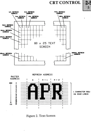
12V supply.The Apricot computer is capable of displaying bit mapped images with a resolution of 800 pixels horizontally by 400 pixels vertically. In the character mode, a text display area of 80 characters by 25 lines is available, using a character cell of 10 pixels by 16 pixels. The video attributes in the character mode are:
3. Keyboard 4. Microscreen tm
5. 'Touch Sensitive Keys 6. Fbt.ed Function Keys 7. Door 8. BrightnesS control
1
11
9. Video Cable 10. Keyboard Cable 11. Keyboard Connector 12. Centronics Connector 13. Serial Connector 14. Video Connector 15. Mouse Port 16. Mains Switch 17. Fuse
18. Mains Input
16
18
[image:25.426.53.382.37.589.2]17
r - - - - 1 r - - - -1
I FLOPPY DISK I FLOPPY DISK I PlW'lTER I
DRIVE DRIVE
I I I I
L
-11-
....J ... L,- .. ::>"'<,..-
....JSYSTEM BOARD _ ... ... ... ...
f"LII'Py DISK PARALLD. PRJrITER cartTRII.J.£R JlffERf'M:£
..
..
..
..
..
.....
,....
i"- ..i"-lIA. TJPRIIC[SSlHG IA
EL.DIOtTS , DAT" JUS ~
~
U
111086 CPU I ADIII£SS IUS j
-~
r--~s
I 8089 lIP I A -
r--- - UItTIIIIL IUS f -r - - - , I'
L!"!. '!" ..J
... ~ ... ... ... :.- ... :.- ... ... ...
[image:26.427.56.359.34.436.2]:.-PRtJiI 256K IIRAH
KEYBOARD UNIT IIUCRIISCRmII
[image:27.421.59.370.75.429.2]IMl~RI
...
c:=
~
-~
c:=
--
-.. !;or .. !;or . . . .
I
Dl'NISIII1 SLDTS
(>12)
\ra:tltl
Jll\TA IUS
AIIDR£SS JUS
aJrfTIItL JUS
I
SDIItI GEItEltATtit
..
...
. . . !..
DISPLAV
carntILLEIt
l
I
Figure 2b. Apricot Computer block diagram
DISPLAY
INTRODUCTION ... ... ... ... .... ... ... ... ... 1 BIOS FEATURES - OVERVIEW OF CAPABILITIES ... 2 Foreground and Background Operations ... 2 Multi-sector Reads and Writes ... 3 Tri-buffer ... 3 Apricot Control Device ... 4 System Configuration Block ... 4 MicroScreen Driver ... 4 Time and Date Clock ... 5 Calculator ... 5 General Hardware Support ... 5
INTRODUCTION
The control software for the Apricot Computer consists of two modules: the BIOS and the DOS, collectively referred to as the OPERATING SYSTEM. The BIOS (an acronym for Basic Input Output System) is generally 'in charge' of the hardware in the computer. The DOS (Disk Operating System) is the interface between the user, application program and the BIOS. The DOS is loaded into memory by the BIOS when the system is booted up and then takes control of the entire system. It can be considered as a "black box", which can request various services from the BIOS. For
example, if the DOS wants to print a character on the
screen, it has to interrupt the BIOS and giveit the necessary instructions to carry out the operation.
The DOS is Microsoft's MS-DOS Version 2.0, which has many advanced features to make the running of application software extremely efficient. The BIOS was written by ACT (Advanced Technology) Ltd. specifically to run in
MS-DOS 2.0 is a direct descendant of MS-DOS 1.25 which became widely used on 3rd generation 16-bit
microcomputers such as the ACT Sirius 1, and (as PC-DOS) on the IBM PC. It was written by MicroSoft Corporation, one of the worlds leading micro-computer software houses. Cosmetically similar to CP/M-like operating systems, most of its advantages are with its internal commands, such as UNIX-type features including Piping, tree-structured directories and Background operations.
The BIOS consists of a number of hardware device drivers which MS-DOS makes use of. There are drivers for the keyboard, screen, MicroScreen, communications ports, clock, disk drives, sound and various hardware add-ons. There are also software drivers, which control graphics, background printing, disk cache and calculator.
The BIOS was written in 8086 assembly language and Pascal. Most of the hardware interfacing code, such as the keyboard, video display driver and low-level device I/O was written in assembler, leaving the code which involves large-scale decision making such as the disk handler to be written in Pascal. Insource form, it consists of a number of modules which have to be linked together to form the BIOS.
BIOS FEATURES - OVERVIEW OF CAPABILITIES
The Apricot BIOS is a modular system written using the latest structured programming techniques. It is a fast, efficient piece of code which is capable of making
maximum use of the Apricot's advanced hardware features.
This BIOS has many features implemented over and
above the those incorporated in other 10 systems.
Foreground and Background Operations
The Apricot BIOS has been implemented in such a manner that fully-Hedged "foreground" and "background" processing is supported. That is all hardware operations to and from I/O drivers are buffered and interrupt driven. This
m~kes it possible to use MS-DOS in a real-time
Multi-sector Reads and Writes
The 8089 Input/Output Processor has been programmed to perform submerged (in the 'background' or simultaneous with 8086 operations) disk read and write functions on multiple sectors. This increases the speed of most disk operations and fits into the philosophy of MS-DOS 2.0 multiple driver request operations.
Tri-buffer
1. Disk Cache Memory. The cache memory is used by the
disk driver to hold a number of disk sectors, and operates in the following manner:
Disk READ
Disk WRITE
The disk driver, on receiving a request for a sector to be read, first examines the cache to
find out if the sector is resident in memory. If
resident, the sector is immediately returned to
the DOS. If not resident, the sector will be read
from disk and if there is room within the cache,
the sector is saved, as well as returned to the
DOS. If there is no space, the cache overwrites
the sector image within the cache which has not been accessed for the longest period of time with the new sector.
When a disk write request is made to the disk driver, the sector is written to disk as well as
being saved within the cache. If there is no
space, again the sector image within the cache not accessed for the longest period of time is overwritten with the new one. All sector writes to disk are performed in the background, so the BIOS does not need to wait around until the operation is complete before returning to the DOS. This background operation is possible because of the 8089 lOP and the cache.
2. Print buffer. The Print buffer has the same effect on
As a command is issued by MS-DOS for the Bios to print a character on a connected line printer, the Bios will place this character in a 2K buffer, and returns control back to MS-DOS immediately. When the lines from the printer state that it is ready for another character, the next entry in the buffer is sent to the printer to be printed and room is made in the buffer for another character.
3. Communications buffer. The communications buffer· allows high speed transfer (up to 9.6 kbaud) of data between the Apricot and other computers. The serial driver supports full XON /XOFF protocol to prevent the loss of data when the buffer fills.
Apricot Control Device
This is a software device which enables the programmer to pass parameters to routines in the BIOS for controlling various hardware and software functions without having to resort to assembly language programming. As a result no low-level hardware knowledge of the Apricot is required by applications programmers.
System Configuration Block
The system configuration block is a small block of memory which contains the reference values that the BIOS uses for port characteristics, character sets and keyboard tables. By changing certain parts of this area it becomes easy for the programmer to change the hardware and software configuration of the Apricot.
MicroScreen driver
Time and Date Clock
The time of day clock (located within the Keyboard) has . been fully integrated within the BIOS. So on power up,
MS-DOS will display the correct time and date which can easily be changed with the TIME and DATE commands.
Calculator
From power up, a simple four-function calculator is available without the need to insert a disk. This calculator can also be accessed from within an application and results of calculations can be sent to the screen as if they were typed in from the keyboard.
General Hardware support
The BIOS also supports the Apricot hardware to a greater extent than on other systems:
The Keyboard. Each of the keys on the Apricot keyboard can
be made to produce up to three different codes, when pressed in the Unshifted, Shifted or Control modes. These codes can be:
1. A single character.
2. A string of characters, maximum length 255. 3. A number of prefix codes can be sent, such as ESCAPE.
4. The key can be defined as LOCAL, where its output is sent directly to the screen driver.
5. The key can have a combination of attributes, where it can be affected by the CAPS lock, or SHIFT lock
modes. .
6. An auto-repeat mode can be selected where a depressed key continues producing its code until released
Screen Driver. The screen display is totally compatible with
the Sirius. All the escape codes can be used directly, and the screen buffer is physically in the same place within
high intensity, strikeout) are supported. Also included is the ANSI escape sequence set, (which is IBM PC compatible) allowing extremely advanced screen modes such as windowing and left and right scrolling to be incorporated within applications.
Character sets. The character set cell is Sirius Compatible, using the fulllOx16 matrix, with shapes easily changed by using the Font Editor.
Communications. An auxilliary serial RS232 and a parallel Centronics-compatible port, fully supported within the BIOS, ensure that the Apricot immediately has access to many hardware add-ons such as printers, plotters and modems.
Graphics. The Digital Research Graphics System Extension,· fast becoming the "industry standard" graphics application software is fully supported.
It has its own application interface in the form of a
INTRODUCTION .. ... ... ... ... ... ... 1 FLOPPY DISK OPTIONS .. ... ... ... ... 1 128 KBYTE RAM BOARD ... ... ... ... ... .... 2 MODEM ... 2 NUMERICDATAPROCESSOR ... 3
INTRODUCTION
NOTE: All options are installed internally within the Apricot. This task must only be undertaken by a qualified dealer or a trained service engineer.
The basic configuration of the Apricot Computer can be altered by the addition of various hardware options to reflect the differing requirements of the user. These hardware options are listed below and described in greater detail in subsequent paragraphs.
(a) Floppy disk drive options. These include the addition of a second 3.5 inch disk drive and also utilising 3.5 inch disk drives which use MicroFloppy disks with a total storage capacity of 720 Kbytes of formatted data.
(b) 128 Kbyte RAM expansion boards. (c) Modem.
(d) Numeric Data Processor.
FLOPPY DISK OPTIONS
A second 3.5 inch floppy disk drive which uses single sided disks with a storage capacity of 315 Kbytes of formatted data can be fitted into the System Unit without any modification to the existing hardware, to provide a dual MicroFloppy disk drive system. Each disk has 70 tracks and is soft-sectored employing the IBM system 34 format in the double density mode with 512 bytes per sector and 9 sectors
An alternative version of the 3.5 inch floppy disk drive can be installed within the System Unit, as a direct
replacement for the floppy disk drives described above. This alternative provides an increase in the size of the floppy disk storage space available.
The alternative version uses 80 track double sided disks (i.e. 160 tracks per disk) and also employs the same format, mode and sector size as detailed above. Each disk has the capacity to store 720 Kbytes of formatted data, producing a corresponding increase in total disk capacity for a dual MicroFloppy disk drive system to 1.44 Mbytes.
128KBYTE RAM EXPANSION BOARD
The 128 Kbyte RAM Expansion Board fits into the expansion slots within the System Unit. Both expansion slots can accommodate the RAM board, thus providing an increase in the size of the RAM within the Apricot to either 384 Kbytes (one board), or 512 Kbytes (two boards).
MODEM
The Modem option is a communications facility to allow an Apricot computer to transmit and receive data via the Public Switched Telephone Network (PSTNj. The option is installed within the Apricot by inserting the Modem Board into one of the expansion slots and making a minor
modification to the rear panel of the System Unit to replace the expansion plate.
The Modem Board consists of a modem and a
microprocessor control system. The modem conforms to both CCITT V23 and V21 standards and operates in anyone of the following software selectable modes:
(a) Full duplex 1200/75 bps. (b) Full duplex 300/300 bps. (c)Half duplex 1200/1200 bps.
autodialler facility. Telephone numbers can be "dialled" via the Apricot keyboard, transferred to the microprocessor control system on the Modem Board and retained in its internal memory. Automatic dialling of the number stored in modem memory, is performed under the control of the Modem microprocessor.
NUMERIC DATA PROCESSOR
The Numeric Data Processor (NDP) option is an Intel 8087 16-bit microprocessor which can be fitted onto the System Board within the System Unit to extend the processing capabilities of the Apricot in mathematical and scientific applications. The NDP is a simple plug-in item which fits into a socket already provided on the System Board.
The NDP acts as a co-processor to the 8086 central processing unit (CPU), and fits into the local
multiprocessing configuration on the System Board. In effect, the NDP provides an extension of the instruction set of the CPU, allowing the Apricot to perform arithmetic computations and comparison operations on numeric types of varying size from 16 to 80 bits. In addition to arithmetic and comparison operations, the NDP also executes
HARDWARE DETAIL
SYSTEM UNIT ... 2-1 SYSTEM BOARD ... ... 2-2
INTERRUPT CONTROLLER ... 2-3
INTERVAL TIMER ... ... 2-4 CRT CONTROL ... ... 2-5
FLOPPYDISKINTERFACE ... 2-6
SERIAL INTERFACE ... 2-7 PARALLEL INTERFACE ... 2-8
SOUND GENERATION ... 2-9
EXPANSION SLOTS ... 2-10 DISK DRIVE ... 2-11
KEYBOARD ... 2-12
INTRODUCTION ... 1
SYSTEM BOARD ... 2
DISK DRIVES ... 3
POWER SUPPLY DETAILS ... 3
General ... :... 3
DC Supply Distribution ... 4
Fuse rating ... 4
PHYSICAL DIMENSIONS ... 5
List of Illustrations Figure
System Unit external detail ... 1 System Unit internal detail ... 2
INTRODUCTION
The System Unit is the area of the computer, which houses the processors, the system memory, disk drive(s), the Power Supply Unit, a cooling fan and all the interface circuitry for connecting the Keyboard, Display Unit and other peripheral equipment.
All the electrical and electronic components are contained internally within the plastic cas,e. A shallow recess at the top of the case is provided for the Display Unit.
The Unit is designed for ease of transportation, incorporating a carrying handle which slides out from underneath the disk drive(sl, and a sliding cover to prevent dust or any other objects entering the disk drive inputs during transit. The Keyboard can also be carried attached to the underside of the System Unit, utilising the clips
Connectors for the Keyboard, the Display Unit, the mains input and other peripheral equipment are all located on the rear panel of the Systems Unit. The connectors from left to right when looking at the rear panel are as follows:
1. The Keyboard connector (9-pin female D-type).
2. A parallel printer port (36-way female Centronics). 3. An RS232C communications port (25-pin female D-type).
4. The Display Unit connector (9-pin male D-type).
Also included on the rear panel is the mains switch and the mains input fuse. The indicator on the switch is illuminated when the Systems Unit is switched on.·
Two plastic expansion plates are located above the
Keyboard connector on the rear panel. These are removed to allow external equipment to be connected to the expansion boards with a minimum of modification to the rear panel.
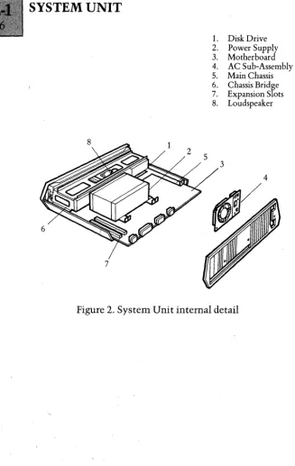
All the processing circuitry is contained on a single printed circuit board, the System Board, which fits horizontaJly into the base of the Systems Unit. Located above the System Board inside the Unit, is the Power Supply Unit, a loudspeaker and either one or two disk drives. The cooling fan is attached to the inside of the rear panel.
SYSTEM BOARD
The System Board incorporates:
(a) The system processors. (b) The Boot Proms.
(c) Thesystem memory (256 kbytes of dynamic RAM). (d) TwoExpansion Slots.
(e) Circuitry for controlling the monochrome Display Unit.
(f) A dual channel Serial Interface, one channel for communicating with peripheral equipment via an RS232C link, one channel for keyboard
communications.
A description of the System Board and all the major
circuit elements on the board listed above are detailed in I
subsequent chapters.
DISK DRIVES
One or two disk drives can be fitted inside the System Unit. In a single drive system, the disk drive is fitted on the left hand side (as viewed from tile front). Single drive systems can be upgraded into a dual drive system by adding a second disk drive without any modification to the
hardware.
The disk drives are mounted on a metal chassis assembly above the System Board, and secured in place by two pairs of screws in each of the chassis side plates. The disk eject button and the activity indicator of the disk drive fit through the front facia of the System Unit. The function of the disk eject button is self-explanatory. The activity indicator is illuminated when disk read and write
operations are in progress, and also momentarily when the disk is first inserted into the drive.
A ribbon cable assembly connects the disk drive to the disk interface on the System Board. Regulated power
supplies are supplied to the drive from the System Board, via a 4-way cable assembly.
The standard disk drives use 70-track single sided
MicroFloppy disks with a total storage capacity of 315
kbytes of formatted data. A detailed description of these disks and further details of the disk drives can be found in the Disk Drive section.
POWER SUPPLY DETAILS
General
The power supply unit is of switched mode design, providing regulated outputs of + 12V, +SV and-12V for use by the System Board, the Keyboard, the disk drives, the Display Unit and any expansion boards fitted. The power supply components are housed in a shielded case. A fuse is located in the mains input line, internally within the unit.
DC Supply Distribution
The regulated outputs from the PSU are supplied to the System Board via a 7-wire cable assembly, terminated at both ends in Molex connectors. The PSU provides two separate regulated supplies of + 12V, a single regulated supply of +SV and a single regulated supply of -12V. The maximum current rating for the four supplies are detailed below. The "V" prefix corresponds to a pin/number of pins on thePSUDC connector.
VI (+SV supply) 6.0A V2 (+ 12V supply) l.SA V3 (+12Vsupply) 2.1A V4 (-12V supply) O.2SA
Distribution of the supplies from the System Board to the other areas are via the board wiring to the appropriate connector. The board provides:
1. + 12V to the Display Unit via the Display Unit connector.
2. + 12V and -12V to the Keyboard via the Keyboard connector.
3. + 12V, +SV and -12V to the expansion connectors. 4. + 12V and +SV to the disk drive(s) via Molex connectors and 4-wire cable assemblies.
Fuse rating
The rating of the fuse on the rear panel of the System Unit is dependent on the mains input voltage, as detailed below.
PHYSICAL DIMENSIONS
5
Height: 4.0 inches
Width: 16.5 inches
Depth: 12.5 inches
Weight: 14.2lbs (Dual disk drive version, single disk drive version, 1.5lbs less).
2
1
~4
9 8
1. Systems Base 2. Systems Cover 3. Rear Panel 4. Facia Bezel 5. Door
6. Expansion Plates 7. Handle
8. Base Clip 9. Base Button
[image:42.424.61.373.206.560.2]10. Keyboard Cable Clips
Figure 1. System Unit External Detail
6
1. Disk Drive 2. Power Supply 3. Motherboard 4. AC Sub-Assembly 5. Main Chassis 6. Chassis Bridge 7. Expansion Slots 8. Loudspeaker
[image:43.427.34.361.41.558.2]INTRODUCTION ... '" ... ... .... 1
DESCRIPTION .. ... .... ... ... ... ... ... ... 1
Processors . .. . ... .. ... .. . ... .... .. .. . . .. .. .... . ... ... .... ... .... .. 1
Communications Handling ... 2
Sound Generation ... 3 System Memory ... 3
CRT controller ... 4 Floppy Disk Controller ... 4 Expansion Slots ... '... 4
Interrupt Controller ... 4 Timer ... 4
Input/Output Space ... 5
INTRODUCTION
The architecture of the Apricot System Board can be split into 9 main sections, as detailed below:
1. Processors
2. Communications 3. Sound Generation 4. System Memory 5. Expansion Slots 6. CRT control
7. Floppy Disk control
B. Interrupt Handling
9. Timer
DESCRIPTION
Processors
The Apricot has, as standard, two 16-bit processors: the
Intel BOB6 microprocessor and the Intel BOB9 I/O processor.
Available as an option is the BOB 7 Mathematics
8086. The 8086 processor is directly language-compatible with the 8088 processor which is used on many 3rd
Generation machines. It runs at a clock speed of 5 MHz,
typically executing 1.4 million instructions per second, and has a 16-bit data-bus which enables it to read and write words into memory in one access as opposed to two with the 8088.
8089. The 8089 is an I/O processor and two-channel DMA
device which is used mainly for disk reads and writes. It has
the capability to transfer data from memory to memory, memory to port, port to memory and port to port
8087 (optional). The 8087 mathematics co-processor is used
in parallel with the 8086. Full floating-point and intrinsic arithmetic is supported and the 8087 has its own
instruction set which in effect extends the instruction set of the 8086.
Communications Handling
The Apricot has two peripheral ports, a parallel printer port driven by the Intel 8255 PIO, and a serial
communications port driven by the Zilog Z80 SIO.
Z80 SIO. The Z80 Serial I/O Controller has two
independant full-duplex channels with separate control and
status lines for modems or other devices. Data rates from
a
to SOaK bits/second can be accomplished. Full Synchronous and Asynchronous control is provided, but the current BIOS only supports Asynchronous protocols. In the Async mode, 5,6, 7 or 8 bits/character and variable stop-bit configuration is available. Also included is Break Generation and
detection, parity, overrun and framing error detection. The controller itself also has interfacing for daisy-chain
interrupt vectoring without external logic.
8255A-5 PI~. The 8255 Parallel Input/Output interface
provides the communications interface between the Apricot and an external printer, via the Centronics connector. It also produces a series of control outputs to various areas of circuitry under software control. Though bi -directional communication is supported in hardware, the current BIOS only uses the standard form of
Sound Generation
The Apricot uses the Texas Instruments SN 76489 sound generator, which consists of the following major
components:
1. Three programmable tone generators, each with
associated control registers. (Tone generators I, 2 and
3).
2. A single programmable noise generator with associated control registers.
3. An 8-bit parallel interface for transferring data from the data bus to the control registers.
4.An Audio output buffer stage.
Within the BIOS, the sound generator is used for keyclick (using the noise generator) or the "bell" tone (using one of the tone generator channels).
Systenn ~ennory
Address (hex) Utilisation
00000 - 3FFFF Standard RAM
40000 - EFFFF RAM Expansion
FOOOO - FOFFF Screen Buffer
F1000 - F7FFF Unused
F8000 - FBFFF Unused
Feooo - FFFFF Bootstrap ROM
The standard System RAM consists of 32 64k x 1 bit DRAMs, arranged in two blocks of 128Kbytes.
The RAM expansion is by way of the Expansion Sockets.
The Screen Buffer RAM is located in two separate Static RAM units.
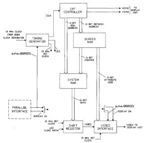
CRT Controller
The CRT control circuitry is, centred around the Motorola 6845 CRT Controller. The hardware can be
software configured for either standard 80 x 25 text mode, or 800 x 400 pixel graphics.
Floppy Disk Controller
The Floppy Disk Interface is the Western Digital
WD2797-02 FDC, a series of buffers, a decoding circuit and the interface connector. Extensive use is made of the 8089 I/O Processor when reading and writing to disks.
Expansion Slots
The Apricot has two expansion slots which are
essentially extensions of the standard system address, data and control busses.
Interrupt controller
The Intel 8259A Programmable Interrupt Controller (PIC) forms the interface between the devices capable of
generating interrupt requests and the interrupt control line of the 8086 processor.
Timer
Input/Output Space
All the peripheral components located on the board are mapped into the Input/Output space, with address locations allocated as detailed below.
DEVICE I/O ADDRESS LOCATION
(Hexadecimal)
PIC 0,2
FDC 40, 42, 44, 46
PIO 48, 4A, 4C, 4E
SOUND '50
GENERATOR
TIMER 58, SA, 5C, 5E
SIO 60, 62, 64, 66
CRTC 68,6A
8089 70,72
EXPANSION 80 to IFFF
INTRODUCTION . ... ... ... .... .... ... ... ... ... 1
DESCRIPTION ... 3
General ... 3
Interrupt Sequence ... 4
Interrupt Masking ... 5
PROGRAMMING CONSIDERATIONS ... 5
General ... 5
Initialization Command Words ... 6
Operational Command Words ... 8
List of Illustrations Figure
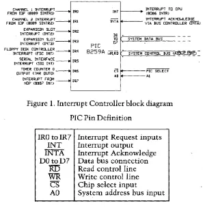
Interrupt Controller block diagram ... 1
INTRODUCTION
The Intel 8259A Programmable Interrupt Controller (PIC) forms the interface between the devices capable of
generating interrupt requests and the interrupt control line of the 8086 processor (CPU on the System Board). Interrupt requests are supplied to the PIC, when the device requires an associated service routine to be undertaken.
CHANNEL 1 INTERRUPT IRO INT INTERRUPT T[] CPU
FROM IDP (8089 SINTRD (8086 INTR)
CHANNEL 2 INTERRUPT
IRl INTA INTERRUPT ACKNOWLEDGE
FROM IDP (8089 SINTR2) VIA BUS CONTROLLER (INTA)
EXPANSION SLOT IR2
INTERRUPT (INT2) DO
EXPANSION SLOT
IR3 TO SYSTEM DATA BUS
INTERRUPT (INT3) prc D7
FLOPPY DISK CONTROLLER
INTERRUPT (FDC INT) IR4 8259A WR:RIi SYSTEM CONTROL BUS <AI~~.~):= SERIAL INTERFACE
IR5 INTERRUPT <SID INT)
TIMER COUNTER 0 IR6 cs PIC SELECT
OUTPUT <TMR OUTO)
AO Al
[image:50.426.59.362.78.385.2]INTERRUPT FROM IR7 NDP (8087 INT>
Figure 1. Interrupt Controller block diagram
PIC Pin Definition
IRDtoIR7 INT INTA DDtoD7
RI5
WR CS AD
Interrupt Request inputs Interrupt output
Interrupt Ackno-wledge Data bus connection Read control line Write control line Chip select input
DESCRIPTION
General
The device connections to the interrupt request lines of the PIC are illustrated on the block diagram on Figure land expanded in more detail below. An active interrupt request is indicated by a logichigh state on the appropriate request line.
8089 Interrupt from Input/Output Channell of the
SINTRl 8089 Input Output Processor (lOP).
8089 Interrupt from Input/Output Channel 2 of the
SINTR2 8089 Input Output Processor.
INT2 Interrupt control line wired to both Expansion
Slots.
INT3 Interrupt control line wired to both Expansion
Slots.
FDC INT Interrupt from the Floppy Disk C'ontroller.
SIO INT Interrupt from the SIO of the Serial Interface.
TMR
OUTO
Output from Counter 0 of the Programmable
Interval Timer (TMR). .
The system software views the PIC as two input/output
ports, with each port able to accept and provide a vari~of
data bytes. The port address locations, defined by the PIC select line and the system bus connection, together with the abbreviations of the data bytes are given below. A detailed explanation of the data can be found in the
PROGRAMMING CONSIDERATIONS section following.
Port Address Data Bytes Transfer Operation
0 IRR/ISR Read
0 ICWl/OCW2/0CW3 Write
1 IMR Read
1 OCWI/ICW2/ICW4 Write
Interrupt Sequence
The interrupt sequence, entered on receipt of a logic high on any of the interrupt request lines of the PIC is described in the following paragraphs. This sequence is the same regardless of the actual PIC interrupt request line being set active.
When one or more of the interrupt request lines are set into the active high state, corresponding bits in an 8-bit internal register within the PIC (the Interrupt Request Register-IRRj are also set. The PIC selects the highest priority bit stored in the IRR, which is not masked by the software, for comparison with bits stored in a second 8-bit register (the Interrupt Service Register-ISRj, to determine whether an interrupt should be issued to the CPU.
The Interrupt Service Register contains bits which indicate the interrupt service routines currently being
executed by the CPU. If the highest priority unmasked
interrupt request is of a higher priority than the highest priority bit set within the ISR, the interrupt control line to
the CPU is set into the active state. If the highest priority
Providing the software controlled interrupt-enable flag of the CPU is enabled, the CPU acknowledges the interrupt, by issuing two Interrupt Acknowledge pulses (INTApulses) to the PIC, via the 8288 Bus Controller. The first INTA pulse latches the highest priority interrupt request from the
IRR through to the ISR. The second
INTA
pulse enablesvectoring data associated with the highest priority bit within the ISR onto the system data bus.
The vectoring data (designated an interrupt number) is a single software defined byte, which is used by the CPU to specify the address location of the corresponding service routine. On completion of the service routine, the
associated ISR bit within the Interrupt Service Register is reset under software control.
Interrupt Masking
Masking any of the interrupt requests is achieved under software control by utilising a third internal8-bit register located within the PIC, known as the Interrupt Mask Register (IMR). The 8-bits within the IMR directly correspond to the 8-bits within the Interrupt Request Register. Setting an IMR bit prevents the PIC actioning any active state on the associated interrupt request line.
PROGRAMMING CONSIDERATIONS
General
Before the PIC can operate normally within the processing system, it has to be initialized with a series of command words which define the required operating mode, the vectoring data and the initial priority of the interrupt request inputs.
Once initialised, the operation of the PIC can be modified and controlled by a second series of command words which:
(a) Enable the interrupt request lines to be individually masked.
(c) Enable the priority of the interrupt request lines to be changed.
(d) Allow the status of the bits of the three internal registers within the PIC (IRR, ISR and IMR) to be analyzed.
The first series of command words are called Initialization Command Words and the second series, Operational Command Words.
Initialization Command Words
Three Initialization Command Words (ICWs) are required to set the PIC into an initial operating condition. The three
words have to be issued in a fixed sequence, and if any
changes to the initial operating condition are required, the whole sequence must be reprogrammed. Once initialized; the priority of the interrupt requests are automatically assigned from IRO (highest priority) through to IR7 (lowest priority); the PIC is able to accept interrupt requests.
The initialization programming sequence is ICWl first, ICW2 next, and finally ICW 4. ICW3 is not required since the system operates using a single PIC.
ICWl defines two parameters when the PIC is used with an 8086 CPU. These are as follows:
(a) The way the PIC senses an active interrupt request (either edge or level sensitive interrupt request). (b) Whether there is more than one PIC operating within the processing environment.
Due to the fact that the two interrupt request lines from the Expansion Slots are connected to both Expansion Slots (in effect in wire-ORed fashion), the level sensitive interrupt mode must be adopted. (In the edge sensitive mode, a
transition on an interrupt request line from a device connected to one of the Expansion Slots would be
undetected by the PIC, if the interrupt request line is
Since the PIC has to respond to a level sensitive interrupt request and there is only one PIC, the format of ICWl is fixed as detailed below. The address location ICWl is written to, is OOH in the system input/output space.
D7 DO
x indicates that the logic state is immaterial program to zero.
The function of ICW2 is to define a base address for the interrupt number. This is signified by five bits within the control word. The three other bits required to form the whole interrupt number (the 3 least significant bits - LSB) are auto.matically inserted by the PIC and are dependent on the interrupt request line as detailed below.
IR T2 Tl TO
0 0 0 0
1 0 0 1
2 0 1 0
3 0 1 1
4 1 0 0
5 1 0 1
6 1 1 0
7 1 1 1
T* = Interrupt Number bit
The base address of the eight interrupt numbers assigned to the PIC is SOH as defined by the ICW2 format below. The I/O address location ICW2 is written to, is 02H.
T7 T6 T5 T4 T3
assigns the following interrupt numbers to the interrupt request lines.
IR Input Type Vector
0 lOP SINTRl SOH
1 lOP SINTR2 5lH
2 INT2 52H
3 INT3 53H
4 FDC INT 54H
5 SIO INT 55H
6 TMROUTO 56H
7 NDP INT 57H
The majority of the features provided by ICW4 are for use with systems utilising more than one PIC and therefore not relevant to the single PIC environment operated on the System Board. The command word still has to be issued, to provide the PIC with the following information:
(a) The associated CPU is an 8086 device.
(b) Termination of an interrupt service routine is to be signified by software using an Operational Control Word, and not by the automatic end of interrupt
facility (AEOI), available during the hardware interrupt acknowledge cycle. (AEOI is only suitable for systems with interrupts which occur at a predetermined rate).
The required format for ICW 4 is as detailed below and is written to the address location 02H in the system input/ output space.
I
0I
0I
0I
0I
0I
xI
0I
1I
ICW4Operational Command Words
modified using anyone of three Operational Control Words (OCWl, OCW2 or OCW3). The OCWs are not dependent on each other and can be issued at any time during program execution.
OCWl provides the facility for enabling/disabling individual interrupt request lines. This is achieved by issuing the control word to the 8-bit Interrupt Mask Register (IMR) within the PIC. The address location of the IMR is 02H within the system input/output space and the format of OCW 1 is as follows.
I
M71 M61 M51 M41 M31 M21 Ml
I
MO
I
DeW1Each bit within the IMR directly corresponds to an interrupt request line (MO of the IMR affects IRO, Ml of the IMR affects IRl, M2 affects IR2 etc.).
Interrupt request lines are disabled (masked) when the corresponding bit within the IMR is set to logic high, and enabled (not masked), when the corresponding bit is set to logic low.
The status of the bits within the mask register can also be read by the programmer at address location 02H within the I/O space.
OCW2 is a dual purpose control word, which allows the priority of the interrupt requests assigned during the initialization sequence to be altered, and is also used to inform the PIC that an interrupt service routine is terminating.
The facilities prilvided by OCW2 for altering the priority of the interrupt requests are not required, since the actual hardware IR connections have been made on the basis of the priority assigned during the initialization routine.
Register), is as detailed below. The address location OCW2 is written to, is OOH within the I/O space.
OCW3 is a command word which provides more facilities to alter the priority of the interrupt request lines, and also allows the status of two internal registers within the PIC, the Interrupt Request Register (IRR) and the Interrupt Service Register (ISR), to be checked. Facilities for altering the priority of the interrupt request lines are not required as explained above.
To read either of the two registers requires two operations to be carried out; a write operation using OCW3 to select the register; followed by a read operation to access the data within the register. The format of OCW3 to select the registers is detailed below. The address location of OCW3 is OOH within the I/O space. The address location, the register data is read from is also OOH within the system input/ output space.
I
xI
0I
0I
0I
1I
0I
1IRIsl
OCW31 - Read ISR
INTRODUCTION ... .... ... ... ... ... ... 1
DESCRIPTION ... ... ... ... ... ... 2
General ... 2
CounterO ... 5
Counter 1 and 2 ... 6
Baud Rates ... 8
List of Illustrations Figure
Programmable Interval Timer block diagram ... 1 Mode 0 timing diagram ... 2 Mode 3 timing diagram ... 3
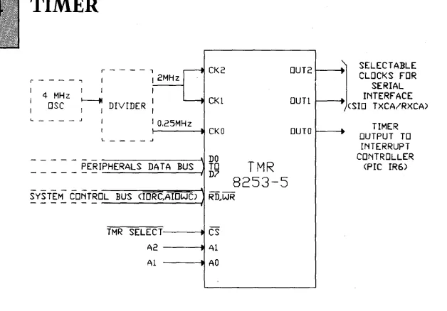
INTRODUCTION
The Intel 8253-5 Programmable Interval Timer (TMR) is located on the System Board. The timer utilizes two clock inputs from a divider circuit to generate:
CK2 OUT2 r - - - - . , I
I 4 MHz I I I
I OSC ~ DIVIDER : CKI OUTI
IO,25MHz
CKO OUTO
- - - \ 1 DO
_ _ _ _ _ ~E~IPHERALS DATA BUS TO T M R
D7 8253-5
~Y~T~~ ~O~T§O-L-B-U-S -(l=O=RC-',A-ro-W-C--"')I Ri),WR
TMR SELECT CS
A2 Al
Al AO
~
SELECTABLE CLOCKS FORSERIAL INTERFACE (SID TXCA/RXCA)
TIMER OUTPUT TO
INTERRUPT CONTROLLER
[image:60.422.45.359.42.261.2](PIC IR6)
Figure I.Programmable Interval Timer block diagram
TMR Pin Definition
CKO CKI CK2
OUT 0
OUT 1
OUT 2
DOtoD7 RD WR CS AO,AI DESCRIPTION General
Clock input for Counter 0
Clock input for Counter 1
Clock input for Counter 2
Output from Counter 0
Output from Counter 1
Output from Counter 2
Data bus connection Read control line Write control line Chip select input
System address bus inputs
The timer is organized internally as three independent I6-bit counters, each with an associated control word register which determines the operating mode of the I6-bit counter. The counters count down on the negative edge of
The system software views the three counters and the control word register set as an array of peripheral input/ output ports. The port address locations defined by the timer select and system address bus connections are detailed below:
Port Address Data
Counter 0 58H Count state 0
Counter 1 5AH Count state 1
Counter 2 5CH Count state 2
Control word register set 5EH Control word
Data can be written to all four address locations but can be read only from the three counter locations. Each counter has to be initialized with the required mode of operation, the count state format, and the number of bytes in the count state, using the control word, prior to loading the count state. The counters begin counting downwards on completion of the count state load operation. The count state can be one or two bytes. The format of the control word is as follows:
Control Word Format
07 DO
I sCllscoIRLI\RLo\M2\ MI \ MolBCD \
IT
~counter
formatL
ModeCount state byte operation
' - - - Control word selection
Control word selection
SCI SC2
0 0 Counter 0 0 I Counter I I 0 Counter 2
Count state byte operation
RLI RL2
0 0 Latch count state into storage register 0 1 Read/load most significant byte only 1 0 Read/load least significant byte only 1 1 Read/load least significant byte followed
by most significant byte.
Mode
M2 Ml MO
0 0 0
0 0 1
x 1 0
x 1 1
1 0 0
1 0 1
Mode 0 Interrupt on terminal count Mode 1 Programmable one shot. Mode 2 Rate generator
Mode 3 Squarewave rate generator Mode 4 Software triggered strobe Mode 5 Hardware triggered strobe
Counter format
BCD
Binary Counter BCD Counter
Initializing a selected counter requires the control word to be assembled as detailed below and then written to the control word register set address location.
Counter format
number of bytes
' - - - S e l e c t Counter
condition for loading one byte only into the counter, automatically sets the other byte to zero count state. The counter begins decrementing after the full count value has been loaded.
Two methods are available to read the count values reached by the counters, whilst the counters are counting down. Both methods have no affect on the operation of the counters. The first method is achieved by reading the data stored at the selected counter address location using two consecutive read operations. The first read operation returns the least significant byte of the count state and the second, the most significant byte.
The second method ensures that a stable count state reading is obtained by utilising the control word to latch the count state into a storage register associated with each counter. The count state is then obtained in the same
manner as the first method. (By performing two consecutive
read operations to access the stored count values at the counter address location). To latch the count state into the storage register, the control word is written into the address location of the control word register set, with the format as detailed below.
D7 DO
c=
Logic state ·immaterial 'L...-_ _ _ _ _ Defines latch operation
L...-_ _ _ _ _ _ Selects counter
Counter 0
For the output of Counter 0 (OUT 0) to be used as an interrupt request line to the Interrupt Controller, the
counter must be set to operate in Mode O. When the counter