Rochester Institute of Technology
RIT Scholar Works
Theses
Thesis/Dissertation Collections
11-1-2002
A New electronic image array: The Active pixel
charge injection device
George Lungu
Follow this and additional works at:
http://scholarworks.rit.edu/theses
This Dissertation is brought to you for free and open access by the Thesis/Dissertation Collections at RIT Scholar Works. It has been accepted for
inclusion in Theses by an authorized administrator of RIT Scholar Works. For more information, please contact
.
Recommended Citation
A NEW ELECTRONIC IMAGE ARRAY: THE ACTIVE PIXEL CHARGE
INJECTION DEVICE
by
George S. Lungu
Diploma in Electronics and Telecommunications Engineering,
Polytechnic Institute of Bucharest, 1990
A dissertation submitted in partial fulfillment of the
requirements for the degree of Doctor of Philosophy
at the Center for Imaging Science,
Rochester Institute of Technology
November 2002
Signature of the Author
_
Accepted by _ _
H_e_nry--'-_E_._Rh_o_d....:..y
----'-I_:l~;I_1_7____<~_l)_Z-_
CHESTER F. CARLSON CENTER FOR IMAGING SCIENCE
COLLEGE OF SCIENCE
ROCHESTER INSTITUTE OF TECHNOLOGY
CERTIFICATE OF APPROVAL
Ph.D. DEGREE DISSERTATION
The Ph.D. Degree Dissertation of George S. Lungu has been examined
and approved by the dissertation committee as satisfactory for the
dissertation requirement for the Ph.D. degree in Imaging Science
Dr. Zoran Ninkov, Thesis Advisor
Dr. Lynn Fuller
Dr. Marvin Illingsworth
Dr. Joel Kastner
(t
DISSERTATION RELEASE PERMISSION
ROCHESTER INSTITUTE OF TECHNOLOGY
COLLEGE OF SCIENCE
CHESTER
F.
CARLSON CENTER FOR IMAGING SCIENCE
Title of Dissertation: A New Electronic Image Array: the Charge Injection Active Pixel
Sensor
I, George S. Lungu, hereby grant pennission to the Wallace Memorial Library at R.I.T. to
reproduce my thesis in whole or in part. Any reproduction will not be for commercial use
or profit.
Signature:
_
A NEW ELECTRONIC MAGE ARRAY: THE ACTIVE PIXEL CHARGE
INJECTION DEVICE
by
George Lungu
Submitted
to theChester F.
CarlsonCenter
for
Imaging
Science
College
ofScience
in
partialfulfillment
oftherequirementsfor
thedegree
ofDoctor
ofPhilosophy
attheRochester
InstituteofTechnology
Abstract
This
is
aPh.D.
thesisdissertation in
which a new type ofimage
sensoris
investigated as possible successor to the charge coupleddevice
(CCD)
for
scientificapplications.
power consumption,
low manufacturing
price) and theCCD imager (low
noise,high
dynamic
range).The device
lacks
most ofthedrawbacks
ofthe aforementioneddevices.
A functional array
architecture was created.Based
on this architecture severaldevices
werefabricated.
One
of the arrays wasfully
measured, characterized andsuggestions
for improvement
wereformulated. Most
ofthecharacterization/analysis workdescribed in
thisdissertation
was centered on thefollowing
issues:
temporal noise,linearity
andFPN.
The
measured noiseperformance ofthenewdevice is
excellent and comparableto thenoise performance ofthe scientificCCD.
The newly developed
sensoris necessary for
scientificimaging
applicationsin
spacebased
operation.However due
toits
qualities, thisdevice
couldbe
usedin
amuch wider range of applicationsincluding
commercialdigital
cameras, spectroscopy,ACKNOLEDGEMENTS
I
wishtoacknowledgethreepeoplefor
theirhelp
in completing
thisbody
of work.Without
them,
thisthesiswouldn'thave been
possible.Specifically
I
want to thankDr. Lynn Fuller for allowing
me access to the siliconfoundry
and toall thehuman
and material resourcesin
theMicroelectronics
Engineering
department.
He
providedtraining
in
microelectronics,funding
and advicefor four
yearsin my initial Ph.D.
work.I
acknowledgeDr.
Zoran Ninkov
who was theperson whooriginally
accepted meinto
thePh.D.
program,providing
a goal andtraining
in
solid state sensors;providing
funding
andadvice.He
wasalsothe person whorecommended me to workfor CIDTEC
(Spectra
Physics)
asaway
ofimproving
my knowledge in
thefield.
I
wouldlike
to thankJoe
Carbone for
hiring
me atCIDTEC,
offering
training
in
sensors and
allowing
me accessto stateofthe arttechnology.I
also would alsolike
to thankDr.
Gerrit Lubberts for his helpful mentoring in
theinitial
stages ofthisproject.I
express gratitudetomy
parentsfor persuading
me to pursue adoctoral degree. I
needto mention that
my
motherhad
theinitiative,
anddid
most ofthe workin applying
for
admissionatU.S.
universities.I
wouldlike
to thankmy friend Belinda L. for
the priceless moral support sheTABLE OF CONTENTS
CHAPTER1. SOLID STATE IMAGING ARRAYS BACK- GROUND 1
1.1. Historicalperspective 1
1.2. BasicsON SOLID STATE imaging 5
7.2.7. Photo-generation ofelectric chargeinsilicon 5
7.2.2. ElectricchargestorageintheMOScapacitor 9
1.2.3. Electricchargetransferinsemiconductors 77
1.3. MAINTYPES OF SOLID STATE IMAGERS 12
1.3.1. The CCD 72
1.3.2. Thechargeinjectiondevice
(CID)
imager 191.4. THE (PASSIVE PIXEL)XY-ADDRESSABLE IMAGING ARRAY 31 1.4.1. Thearchitectureofthepassivepixel photodiodearray 31 1.4.2. The workingprincipleofthepassive pixel photodiodearray 32 1.4.3. Advantages ofthepassive pixel photodiodearray imager 32 1.4.4. Limitations ofthepassive pixel photodiodearray 33
1.5. Theacttve pdcel imaging array 34
7.5.7. Thearchitectureofan activepixel
imaging
array 34 1.5.2. The workingprinciple ofthe active pixelphotodiodeimaging
array 35 1.5.3. Advantagesandlimitationsofthe activepixelimaging
array 361.6. NOISEIN IMAGING ARRAYS 37
7.6.7. Photonshot noise 38
1.6.2. Darkcurrent shot noise 39
1.6.3. Reset
(kTC)
noise 401.6.4. Fixedpattern noise
(FPN)
401.6.5. Injectionnoise 41
1.6.6. Thepreamplifier noise 42
1.6.7. Quantizationnoise 45
1.6.8. Noise balance 46
CHAPTER 2. THE LOW-NOISE AP-CID IMAGER 47
2.1. Arrayreview 47
2.2.7. General 53
2.2.2. Thearchitectureof 388x16 Orbit imager 56
2.3. Pixelarchitectures 58
2.3.7. Pixelconfigurationsforthe388x16Orbit imager 60
2.4. Full-framearray operation 63
2.4.1. Modes ofoperation 63
CHAPTER3. EXPERIMENTAL 69
3.1. Imaginghardware 69
3.1.1. Thecamera 69
3.1.2. The
imaging
head 723.2. Transfercharacteristic
(TC)
curve measurements 743.2.1. Background. 74
3.2.2. Experiment 75
3.2.3. Resultsanddiscussion 75
3.3. Gainand noise measurements 77
3.3.1. Method 77
3.3.2. Experiment 77
3.3.3. Resultsanddiscussion 78
3.4. FULLWELL CAPACITY AND DYNAMIC RANGE CALCULATION 79
3.5. LINEARITY 81
3.5.1. Method 57
3.5.2. Leastsquare regression 82
3.5.3. Experiment 83
3.5.4. Resultsanddiscussion 84
3.6. QUANTUMEFFICIENCY 87
3.6.1. Method 87
3.6.2. Experiment 88
3.6.3. Resultsanddiscussion 90
3.7. Darkcurrents
X
935.7.7. Experiment 93
3.7.2. Resultsanddiscussion 94
3.8. Fixedpatternnoise
(FPN)
andshadingmeasurement 963.8.2. Experiment 97
3.8.3. Resultsanddiscussion 97
3.9. Nonlinearityfixed pattern noise
(NLFPN)
measurement 993.9.1. Background. 99
3.9.2. Experiment 99
3.10. Preamplifiercharacterization 101
3.11. Experimentalresults appendix 103
3.11.1. Transfercharacteristic curves 104
3.11.2. Mean-varianceplots 705
3.11.3. Quantum efficiencyplots 706
3.11.4. FPN Results.... 707
3.11.5.
Shading
results 7055.77.6. NLFPNresults 709
CHAPTER 4. PERFORMANCE ANALYSIS AND IMPROVEMENT 110
4.1. Transfercharacteristic curve
(TCC)
1104.1.1. Pixel sensitivityand saturationlevel 770
4.1.2. Gainregions ofthetransfercharacteristic curve 772
4.2. Gainand noise 126
4.3. Nonlinearity 130
4.4. Fixedpattern noise and shading 132
4.4.1. FPNcorrection 752
CHAPTER 5.CONCLUSIONS 142
5.1. Researchobjective 142
5.2. Performancereview 143
5.2.7.
Summary
ofmeasured parameters 1435.2.2. Comparison ofvarious pixel architectures
-guidelinesforan upgradeddesign 144
5.2.3. Goalsaccomplished 749
LIST OF FIGURES
Figure 1.1BasicMOScapacitorandits banddiagrams 70
Figure 1.2 Alongitudinalsectionthroughafour-phase CCD showingtheelectrode structureoftwopixels andthe respective potential wells withinthesilicon
(a),
atransversalsectionthroughthepixelshowingthechannel stops
(b),
and genericwaveformsusedtodrivesuch aCCD. Notethat thepotential well structure representedin(a)
correspondstomoment"t"
indiagram
(c)
75Figure 1.3 Full-frame CCDarchitecture 14
Figure 1.4 AtypicalCCDreadoutstage 75
Figure 1.5 An illustrationoftheworkingprinciplefortheoutput stageofaCCD. Thepreset phase
(a)
andthecharge-voltage conversionphase
(b)
76Figure 1.6 The layout ofand a cross-sectionthroughaCIDpixel 79 Figure 1.7 Across sectionthrougha regionofaCIDpixel covered
by
photogate(a). ThepotentialdiagramoftheMOSstructure
during
inversion(b)
andduring
injection(c). Thisparticulardevice handlespositive charge(holes ina
P-channel)
20Figure 1.8
Working
principleillustration ofatwo-electrodeP-channel CIDpixel. Therighthandsideelectrodeisthesensingelectrode 22
Figure 1.9
Working
principleillustration ofathree-electrodeP-channel CID. Fromlefttorightthefunctionofthe electrodesareasfollowing:sensing, transferand storage 24
Figure 1.10 Blockdiagram ofa genericCIDscanner 26
Figure 1.11 CIDvoltage readout mechanism 27
Figure 1.12 Ablock oftwo-by-twopixelsfora passive-pixelMOS XY-addressablephotodiode
imaging
array(a),and a generic pixel section
(b)
37Figure 1.13 Theschematicofan active pixel photodiode
imaging
array 34 Figure 1.14 Noisesourcesina solid stateimaging
chain 38 Figure 2.1 The first imagestakenwiththe128x128 AP-CIDcamera 49 Figure 2.2Testing
sites atRTFandCIDTECrespectively 49Figure 2.3Photomicrographsofthefirstthreearrays 50
Figure2.4 Photomicrographs of388x16Orbit AP-CIDchip 57
Figure2.5 ReadoutschematicfortheAP-CIDarraysbuilt in fastverticalreadout architecture. Thepixel
schematicis highlighted. 53
Figure2.6 ReadoutschematicfortheAP-CIDarraysbuiltinfast horizontalreadout architecture(MOSIS
Figure2.7 Layoutsketchofthe388x16 Orbit AP-CID chip 57 Figure2.8 Pixel layouts forthreeoftheAP-CID imagers 58
Figure 2.9 Layout ofpixel#3of 388x16 Orbit AP-CID array 67 Figure 2.10 Eight differentpixel configurations usedinthe388x16 Orbit AP-CID 62 Figure 2.11 Thelogic diagram foroperationofafast-vertical scanning 128x128 AP-CIDarchitecture
having
threeelectrodes per pixel 65Figure 2.12 Thelogicdiagram fortheoperationofafast-horizontal scanning 32x32 AP-CIDarchitecture
having
threeelectrodeperpixel 66Figure 3.1 Block diagramand photograph ofthe camerafor388x16 Orbit imager 70 Figure 3.2 Open
imaging
headcase with3-stageTEcooler(a),watercooling setup for 388x16 AP-CIDimaging
head(b)
73Figure 3.3 Transfercharacteristic curvesfordifferentpixel architectures 76
Figure3.4 Amean-variance plotforpixeWl 78
Figure3.5 TCcurvesfortwodifferentpixels,pixeWl(themost
linear)
and pixel#7(oneofthe mostnonlinear) 85
Figure3.6 Variation of nonlinearitywiththeoutput signalrangefordifferentpixel architectures 86 Figure3.7
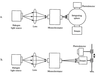
Setup
for measuringthequantumefficiency fortheAPC1D imager inthewavelengthrangeof400nmtoHOOnm
(a)
and300nmto400nm(b)
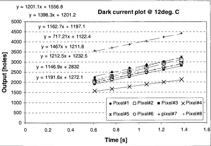
89Figure 3.8 Aphotograph ofthesetupusedforquantumefficiencymeasurements 90 Figure3.9 Quantum efficiencyplotsforvarious pixelconfigurations 97 Figure 3.10 Example ofdarkcurrent
(slope)
estimationat12"C. 93 Figure 3.11 Darkcurrent plots at varioustemperatures:foreachindividualpixel(a),an average persurface
(b)
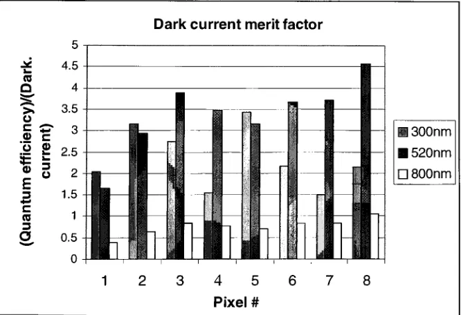
94Figure3.12 Darkcurrentmeritfactor 95
Figure3.13 Fixedpattern noise andshading forpixel#2 98
Figure 3.14
Nonlinearity,
NLFPNandFPNplottedforvariousfractionsofthe maximuminputrange... 100 Figure3.15 Variation of nonlinearity forthepixelpreamplifier 702Figure3.16 PixelpreamplifierFPN. 702
Figure 3.17 Transfercharacteristic curvesfor differentpixel architectures 104 Figure3.18 Mean-varianceplotsfordifferentpixeltypes 705 Figure 3.19 Quantum efficiencyplotsfor differentpixelparameters 706 Figure 3.20 Fixedpattern noise resultsforvarious pixelarchitectures. Therelative exposure means
Figure 3.21
Shading
resultsforvarious pixel architectures. Therelative exposure meanspercentageoftheexposurelevelat saturationfora particular pixel 108
Figure 3.22
Nonlinearity,
nonlinearity fixedpatternnoise, andfixedpattern noise 709 Figure 4.1 Relative sensitivity inredlight fordifferentpixel configurations 777 Figure 4.2 Maximumoutput and sense gate areaforvarious pixel configurations 777 Figure 4.3 Transfercharacteristic curveofa generic3-electrodeAP-CIDhaving
storagegatelargerthansensinggate,exhibitingsevendifferentgain regions 772
Figure 4.4 Apotential wellsdiagramofathreeelectrodeCIDpixel.Genericnamesforfivesignificant volumes within potential wells areindicated. Thenotations ontherightsideofa certainwelllevel
representthephotogate voltagesforwhichthebottomofthepotential well reachestherespectivelevel. 113 Figure 4.5 A diagram showingthechargesharingprocessbetweenthe transferpotential well andthe sense potential well afterthestorage potential welliscollapsed 118 Figure 4.6 Electricchargedistribution beforetheforwardtransferforregionEofTCC 720 Figure 4.7 ChargediagramforregionFbefore forwardtransfer 722 Figure 4.8 TCCplotsofpixel#7forvariousTGvoltages 725 Figure 4.9 Mean-varianceplotforpixel#5. Readoutnoise andtheinjectionnoiseareindicated 727 Figure 4.10 Thedependenceoftheinterceptanddarknoiseofthetotalphotogatearea 728
Figure 4.11 Example of FPNcorrection 755
Figure 4.12 Fixedpattern noise andshadingplotsforfirstorder correctionand secondordercorrection
respectively 756
Chapter 1.
Solid State
Imaging
Arrays
Back
ground
1.1.
Historical
perspective
In
the1960's
there were numerous groupsworking
on solid stateimage
sensorswith
varying degrees
of successusing
PMOS,
NMOS
orthebipolar
process.For
instance,
in
1963
Morrison1reported a structure called
junction
photopot that alloweddetermination
of alight
spot's positionusing
thephotoconductivity
effect.The
mainadvantage of this
kind
ofdevice
was speed (which waslimited only
by
theminority
carrierlifetime). In
the same paperMorrison describes
a similartwo-dimensionaldevice
calledthejunction
scanner.In
1964,
IBM2 reported the scanistor.It
used anarray
of phototransistorsaddressedthrough aresistive networktoproduce an output pulse proportional to the
local
incident
light intensity.
In
1966,
Westinghouse
andNASA
reported a50
x50
elementmonolithicarray
ofphototransistors3.
All
ofthese sensors reported sofar
wereworking in
aninstantaneous
light
to output signalconversionmode.As
aconsequence, thesensitivity
ofthesedevices
was
low.
In
1967,
Weckler
atFairchild
suggestedusing
a p-njunction
in
aphoton-flux-integrating
mode.The
photocurrentfrom
thejunction
wasintegrated
on a reversebiased
p-n
junction
capacitance.The
signal charge,appearing
as a current pulse, couldbe
convertedto a voltagepulse
by
using
aresistor.A
simple methodfor eliminating
thedark
current effectsin
the measurement wasdescribed,
by differentially
reading
out twoIn
1968,
Dyck
andWeckler
report alOOxlOO-element
photodiode array4.Each
pixel contained
both,
abipolar
and aMOS
transistor.The
photodiode wasactually
theemitter-base
junction
of thebipolar
transistor.The MOS
transistor wassimply
a rowselection switch.
The sensitivity
ofthis solid stateimager
outpaced about one order ofmagnitude the
sensitivity
of a typicalVidicon
tube.Weckler later
called thedevice
areticon.
In
1967,
Weimar5 reported a thinfilm
transistor(TFT)
solid-stateimage
sensorusing CdS/CdSe complementary
transistors and photoconductivefilms.
Noble,
in 1968
described
a self-scanned silicondetector
array6.Both,
surface photodiodes andburied
photodiodes
(dark
current reduction) were used.A
chargeintegration
amplifier wasdescribed,
andfor
thefirst
timea sourcefollower buffer in
each pixel was reported.This
architecture
is very
similar to a modernAPS
architecture.Chamberlain
reported animproved
model anddescription
ofthe sensoroperation7
in 1969. He
alsodescribed
thedesign
and measured performance of shift registers,integrated
asdrivers
on the samechip.
Fry,
Noble
andRycroft
exploredtheissue
offixed
pattern noise(FPN)
in
a1970
paper8.
Until recently FPN has been
considered the mostimportant
problem related toMOS
active pixelimagers.
In 1970
whentheCCD
wasfirst
reported9,its
relativefreedom from FPN
wasthe 1 nmain reason
for
its
adoption over themany
otherforms
of solid stateimage
sensors .A
CCD is
ananalog
shift register andit
can alsobe
usedfor
applicationsdifferent
thanimaging.
Since
its
invention
therehave been impressive
improvements
in
theCCD
technology
driven especially
by
thecamcorder market.There have been few
reports aboutmerging
theCCD
andCMOS technologies, but
overall, the subject proved tobe
unfruitful
because
the amountofheat dissipated
by
theCCD
driving
electronics wasvery
large. The
extra steps requiredfor making
aCMOS
processfrom
aCCD
process wouldWhile
alarge
effort was applied to thedevelopment
of theCCD,
Japanese
companies continued the
development
oftheMOS image
sensors10'11
in
thelate 1970's
and
early 1980's. In
1982,
asingle-chip MOS
colorimager
was reported12.The early 1990's
brought
resurgencein CMOS
image
sensordevelopment. Three
separate research groups are
important
tomentionhere:
onein
Scotland
attheUniversity
ofEdinburgh,
onein
Sweden
atLinkoping University
and one attheU.S. Jet Propulsion
Laboratory. The
research of thelast group
was promptedby
NASA's
needfor
highly
miniaturized,
low-power,
radiation-hard,instrument
imaging
systemsfor
next generation13 *
1.1.1. Timeline
oftheAP-CID development
atRIT
The
milestonesin
developing
theAP-CID device
atRLT
arethefollowing:
June 1998
-the
first
active pixelarray (8x8 RIT
AP-CID)
wassuccessfully
fabricated
atRIT
andtestedbased
on adesign
by
G Lubberts.
August
1998
- thesecond active pixel
array (54x40 RLT
AP-CID)
wassuccessfully
designed,
fabricated
andtestedatRIT,
togetherwithG. Lubberts.
November 1998
-the
design
ofthe third active pixelarray (128x128 Orbit
AP-CID)
wascompleted.March 1999
-the
fabrication
ofthe thirdarray
was completed.The array
wastested and proved to
be functional. The first images
with anAP-CID array
were obtained.
June 2000
-the
design
of thefourth array (6x32x32 Mosis
AP-CID)
wascompleted.
The
fabricated device
wasnotfunctional due
toadesign
error.August 2001
-the
design
ofthe388x16 Orbit AP-CID
was completed.February-November
2002
-the
last array
wasbeing
successfully
measured1.2. Basics
on solid
state
imaging
1.2.1.
Photo-generation
of electric chargein
siliconWhen
a photon withenergy
greater than theenergy
band-gap
Eg
of thesemiconductor
is
absorbedinto
thedepletion
region of aMOS
capacitor afree
electron-hole
pairis
created.This
is known
asthephotoelectric effect.Epholon>Eg
(1.1)
h
cphoton photon * \ J
photon
where
h is Plank's
constant,vis
thefrequency,
X
is
thewavelength and cis
the speed oflight. An
important observation canbe
made that thereis
a critical wavelengthbeyond
which photo-generation
doesn't
occur.The
critical wavelengthis
related to thesemiconductor
band-gap
by
thefollowing
formula,
he
1 24
4=7~W
(L3)
Ee
E(eV)
For intrinsic
siliconEg
=1.12 eV andAc=l.ljLlm.
For
extrinsic silicon,energy
levels
canexist within the
forbidden
region,reducing
the effectiveband-gap,
thusincreasing
thecritical wavelength.
A first
order approximationis
the assumption thatany
photon withAfter
photo-generation,theminority
carrierwillbe driven
tothesurface potential minimum and themajority
carrier will moveinto
the substrate.This
way, anisolated
potential well will contain charge, which
is
proportional to the timeintegral
of theincident
optical orinfrared
flux.
1.2.1.1 Types of non-linearity in
theconversion processThere
exist modificationsin
theabove modelfor CCD
sensors, whichdegrade
theefficiency
ofthelight-to-charge
conversion.The
numberof signalchargecarriers createdper
incident
photonis
called quantumefficiency
(n)
or spectral response.Quantum
efficiency is
one of the mostimportant
parameters used to evaluate thequality
of a photodetector andfor
specialdevices it
canbe
greater than one.The
quantumefficiency
depends
onseveralfactors
suchas:Absorption
coefficient(a)
- theabsorption ofthe
light in
a solid cantypically
described
by
Beer's law:
I(x)
=I0-e-x
(1.4)
where
I(x)
represents thelight irradiance
at thedistance
xfrom
the surface.The
absorption coefficient relates to the
probability
ofhow
far into
a material anincident
photon will travel
in
averagebefore
being
absorbedby
thelattice producing ionization.
Absorption
coefficientis
expressedin
units of .The
shorter wavelength(higher
energy) photons are absorbed nearer to the material's surfacethan the
longer
wavelengthphotons,
ff
the absorption coefficientis
toohigh
or toolow,
theminority
carrier canbe
producedin
a region whereit
cannotbe
collected as usable signal, thereforereducing
quantumefficiency.
Recombination
lifetime
(i)
-the photo-induced
minority
charge carrierdensity
decays
in
time
by
recombination.The
time constantfor
this processis
called the recombinationlifetime
x.The
recombination can take placeby
two mechanisms.The
direct
transition ofmechanism not
very
probablein
silicon material.More
probableis
aheat generating
indirect
recombinationmechanism,which occurs throughintermediate
statesbetween
theconduction and the valence
band. These
states are generatedby
impurities,
phonons andlattice
defects.
Typically
a sensoris built
on a silicon waferwhichhas
a"denuded
zone"within the
first few
micronsfrom
the surfacefree from lattice
defects,
while thebulk is
heavy
populatedwith crystaldefects
and wheretheminority
carrierlifetime is very
short.Moreover,
theminority
carrierlifetime
at the silicon surfaceis
reduceddue
to alarge
number of
defects (incomplete lattice bonds
ordangling
bonds)
at the silicon to silicondioxide interface. For
the above reasonsfor both very
short andvery
long
wavelengthsthequantum
efficiency
tends todrop.
Diffusion length
(L)
-Represents
the average
distance
a photo-generatedminority
charge carrier can migrate
before it
recombines. Alarge
valuefor
this parameter rendershigher
quantum efficiency.The
electric chargediffusion
mechanismsin
silicon willbe
treated
later.
However
it
shouldbe
mentioned thatin
a neutral substrate therecombination
lifetime,
% andthe electrondiffusion
length, L,
arerelatedby:
Ln=jD~y
(1.5)
where
Dn
is
thediffusion
coefficientfor
theminority
carriersin
question.Overlaying
films
-in
ordertorealize a
functional CCD image
sensor a stackofpatternedthin
film
materialsis
createdabovethesilicon surface.Typically,
the materials are siliconoxide,polysilicon, silicon nitride, silicides, metals and color
filter
materials.Ideally
these materials would need tobe perfectly
transparentover awide range of wavelengths.From
apractical standpoint, theelectrode structure on the
top
ofthe silicon material presents aconsiderable absorption and reflectance, which
is
afunction
of wavelength.Polysilicon
electrodes aretransparent
for
optical wavelengths greaterthan450
nm, sothatthey
allow thelight
collectionefficiency
tobe satisfactory
exceptfor
a poor responsein
theblue
spectrum, the
illumination
canbe
madeincident
ontheback
surface ofthedevice. A back
illuminated
CCD is built in
a near conventionaltechnology,
except that at the end, asignificant amount ofthe substrate
is
eliminatedby
etching
and polishing.A distance
offew
tens of microns separates the silicon-oxideinterface from
theback
end.This
thickness
has
tobe
comparable with the electrodedimensions
otherwise the randomdiffusion
of charge carriers towards the storage sites will causeimage blurring. This
requirement
usually
ensures that thediffusion
pathis
much shorter than theminority
carrier
diffusion length, ff infrared detection is
required the substrate must notbe
made too thinowing
to the greater thickness of silicon requiredfor
photon absorption, so that the problem ofimage
blurring by
diffusion
remains.Frontal illumination may
well1.2.2.
Electric
charge storagein
the
MOS
capacitorThe
basic
building
block
of aCCD is
theMetal-Oxide-Semiconductor
(MOS)
capacitor, used
both
as alight sensing
element and electrical charge storage element.A
MOS
silicon structureis
shown onFigure 1.4(a). As any
capacitor,it
consists of twoelectrodes, separated
by
aninsulator. One
of the electrodesis
thebulk
silicon.A
thinlayer
ofsilicon oxide(typically
few
tens ofnanometers) serves asdielectric. The
secondelectrode, referred to as gate,
is
placed on thetop
of thedielectric
andis
made out ofmetal or
heavily
doped
polysilicon.The
gateis held
at a voltageV
and the substrateis
providedwith anohmic contactheld
attheground(reference)
potential.Three MOS
structureband diagrams for different
gate voltages are shownin
Figure 1.1
(b,
c,d)
for
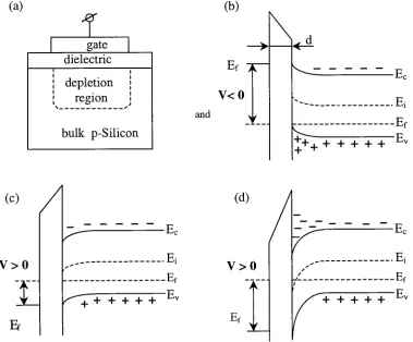
a p-type silicon substrate14.The
accumulation stateis
shownin
Figure 1.1(b). The
negativegatevoltagebends
theenergy bands
upwards andthemajority
carriers
(holes)
areattracted and accumulate at the silicon-dielectricinterface.
Applying
a small voltage asin
theFigure
1.1(c),
theholes
are repelleddeep
into
the semiconductor substrate.A
depletion
regionis
created rightbelow
thedielectric-semiconductor
interface,
where the electron andhole
concentrations are small compared to thehole
concentrationdeep
into
the substrate.This
is
thedepletion
state of theMOS
capacitor.Further increase
ofthe gate voltagebends
theenergy bands
stilldownwards,
creating
apotential well at the
interface,
andattracting
minority
carriers(electrons)
to the surface.At
acertainthresholdvoltagetheelectron concentration attheinterface becomes
equalto thehole
concentrationin
the substrate.This
is
the onset ofthestrong
inversion state, asshown
in Figure
1.1(d).
Any
further increase
of the gate voltageis followed
by
aproportional
increase
oftheelectron concentrationin
thesurfacelayer
atthesilicon-oxideinterface.
This
surface electric chargehas
ashielding
effect on thebulk
of thethereforethewidth ofthedepletionregion willremain constant15.
As
an equivalent circuit thestructurebehaves
similartoaregularcapacitorhaving
thegate oxide asdielectric.
The
holes
generatedin
thedepletion
region are repelledinto
the substrate and collectedby
theback
ohmic contact.The
photo-generated electrons are collectedin
a potential well created at theinterface
by
the potential gradient.The
surface potentialdecreases
with anincrease
of the surface electron concentration and as a result, the potentialwellbecomes
shallower.With time,
thethermally
generated electron-holepairs,constituting
thedark
current, tend tobring
thesystemback
to thequasi-equilibrium state with zero potential gradient,setting
a timelimit for
which theMOS
capacitoris
inversion. The
dark
currentis exponentially dependent
on thetemperature,
so theinversion
statecanbe
extendedby
cooling
thedevice.
[image:23.552.111.490.318.632.2](a)
1
gatedielectric
depletion
regionbulk
p-Silicon(b)
Ef
V<0
and +++ + + + + + EcEi
-Ef(c)
V>0
I
Lv
+ + + + +Ei
-Ef(d)
V>0
"A
+ + + + + ..E -Ef1.2.3.
Electric
chargetransfer
in
semiconductorsThe
movement of charge packets ofminority
carriers throughthe siliconfrom
onegate toanother
is
realizedby
shaping
andreshaping
the potential wells under consecutiveelectrodes.
Charge
transferin
aCCD has
tobe fast
andhighly
efficient.It is very
important
theefficiency
at which the charge-transferoperation takes place.Any
residualcharge
left behind
when a transfer occurs willeventually join
chargebelonging
to otherpixels
causing image blur. The
maximum speed at which charge transfer occurs with agood
efficiency
willdictate
the maximum readout speed of theCCD
array.There
arethree
distinct
charge transfer mechanismsin
aCCD
asdescribed
by
Carnes,
Kosonocky
andRamberg1
:
-thermal
diffusion of
charge carriers : evenin
the absence ofany
electricfield
a charge packethas
thetendency
toredistributetowardsan equilibrium state.-self-induced
fields
:if
thereis any
charge concentration gradient, carriers ofthesametypewill repel each other
determining
chargedisplacement
untilthegradientbecomes
zero.-fringing
fields
: an electricfield
generatedunderthe gate of aMOS
structure canbe
associatedto a potential well.For
smalldimensions
ofthepotential wells whileabutting
gates atdifferent
potentials, the shape of a potential well will nolonger
be
rectangular.Any
deviation
from
a rectangular shape such as rounded edges ortilted
bottom
canbe
associated to an electricfield
component(called
fringing
field)
parallel to the silicon surface.This
componentdetermines
aflow
(drift)
of1.3.
Main
types
of solid state
imagers
1.3.1. The CCD
Till
the end of the1960's,
the physicalimplementation
of the active pixelimage
sensor
had
notbeen very
successfuldue
to thelow-resolution lithographic
techniques,
the reduced yield anduniformity
associated withthefirst integrated
circuits.The
concept ofcharge-coupled
devices
(CCD)
wasfirst
presentedin 1970
by
Boyle
andSmith9. The
newly invented CCD
eliminated thepreviously
mentioneddrawbacks
oftheearly
activepixel sensors.
1.3.1.1.
Charge
storageandtransferA CCD is
ananalog
shift registerin
which photo-generated charge canbe
stored, orcarried
along
the surfacein
potential wells generatedin
semiconductorby
anarray
ofclosely
spacedMOS
capacitors.Voltage levels
applied onthemetalelectrodescontrolthe charge positionin
theMOS array
of capacitors.Under
proper application ofthesevoltagelevels
and their relative phases, thearray
canbe
used to store and transfer the photo-generated charge packets across the semiconductor substratein
acontrolled manner.As
an example, aP-surface
channelCCD imager
is
presented.It
is
a one-dimensionalfour
phase
CCD
array, which means thateach pixel comprise agroup
offour MOS
capacitorseach connected to a
different
clock generator(phase).
The
four
clocks areoverlapping
trapezoidal periodic pulses with the samefrequency
but different delays.
They
create a"moving
well"
effect which carries the photo-generated charge
from
pixel to pixel andprevents the
mixing
of the chargefrom different
pixels.The
chargeis
movedalong
aCCD
channellaterally
defined
by
two channelstop implant
regions.Having
the sameregions cannot
be inverted
by
the voltages on the gates.Therefore
thecorresponding
potentialwellsin
thechannelstop
regions willbe
shallow.04
0 II
\t i >
m&mftwzx^flimaumvmwm
~^~yp
Voltage
t.4
t:
t.
02
Channel stop
(a)
(b)
(c)
^/ \
p
/VU,iPotential
well>
>
[image:26.552.95.503.143.456.2]Time
Figure 1.2 A longitudinal
sectionthrough afour-phase CCD showing
theelectrodestructureoftwopixelsandtherespective potential wells withinthesilicon
(a),
atransversalsection through thepixel
showing
thechannelstops(b),
andgenericwaveforms usedto
drive
such aCCD. Note
that thepotential wellstructurerepresentedin
(a)
correspondstomoment"t"
1.3.1.2.
Architecture
Only
one of the numerousCCD
architectures, which allow particular readouttechniques to
be
employed, willbe
presentedhere. For
atwo-dimensionalCCD
array, afull-frame
architectureis
the simplesttofabricate
and operate,hence yielding
thehighest
resolution and pixel
density. For
this type of architecture, the pixels of thearray
aregrouped
in
an m-wide(m
being
the number of columns) parallel shift registerrunning
vertically.
At
thebottom
(end)
ofthis parallel shift registerthe chargeis
transferred to aserial shift register
having
alength
equal to the number of columns of the array.Therefore,
to one charge transferin
the parallel register, correspond m transfers oftheserial shiftregister.
Because
theparallel shift registeris
usedfor both
scenedetection
andreadout, a mechanicalshutter
is
neededfor
thisparticular architecture.A
Q/V
conv< andampli\l
\l
\l
\l
Y
2f
AL-V-urter
Eier
/
*<
1 V.S:V.S:'/.'7&^nj*Kw^vi.<i^<y>h6h'l'.$:&Out
X^.
_ yJ
Parallel
(slow)
shift
register
Serial
(fast)
shiftregisterAt
the output of thefast
shift register thereis
a charge-to-voltage convertertypically
followed
by
afloating
diffusion
and aMOS
sourcefollower
as avoltagepreamplifier.An
illustration
ofthisarchitectureis
shownin Figure 1.3.
1.3.1.3.
The
readout stageFigure 1
.4 shows the schematicfor
the output stage of anN-channel CCD. The
outputstage of a
CCD is
acharge-to-voltage converter(floating diffusion)
followed
by
apreamplifier,
typically
a sourcefollower (transistor T2).
The CCD handles minority
carriers.While
the photogeneratedmajority
carriersare repelled to the
bulk
by
the electricfield
existent under the gate of a certainMOS
structure
(biased
towardsdeep
depletion),
thecorresponding minority
carriersaccumulateunder the same gate
in
potential wells.This happens in every
pixel,during
light
integration.
TG ^Preset Vec
Figure 1.5 An illustration
oftheworking
principlefor
the output stageof aCCD. The
presetphase
(a)
andthecharge-voltageconversion phase(b).
By
proper manipulation of the voltages on thearray
of gates, this chargeis
clocked towards the outputin
a serialfashion. The last
gate, whichis
also called a transfer gate endsin
a.floating
diffusion,
i.e.
a region ofoppositedoping
type relative to thesubstrate.At
theborder
between
thesubstrate andthefloating
diffusion,
aPN
junction
is formed.
The
charge-to voltage conversionhas
twodistinct
phases.The
first
phase(Figure
1.5)
is
the preset,in
which thejunction
is
set to a reversebias
conditionby
closing
a switch(transistor
Ti),
andthe transfergateis off (biased in
aweakdepletion
mode withthepotential well collapsedunderneath)
The
second phaseis
the charge-voltageconversion whenthediode is left
floating
and
by
turning
the transfergate on,allowing minority
carriers toflow from
the potential wellcorresponding
to thelast
gateofthehorizontal
shiftregisterto thefloating
diffusion.
The
built-in
potential existentin
thejunction
area willdetermine
these carriers toflow
1.3.1.4.
Advantages
oftheCCD imager
Noise: The CCD array has
thebest
noiseamong
all the other categories of solidstate
imagers known
today.Noise
figures
below
one electron r.m.s.using
multiple-readtechniques
have been
reported.This low
noiseis determined
by
thefact
thatchargefrom
each pixel
is
being
driven
to a unique output stage, whichhas
avery high
gain(voltage/charge)
andis
optimizedfor
noiseandlinearity.
Simplicity: The CCD is
theimager
with the simplest pixel structure, and nodriving
circuitry necessary
onchip.Size:
Very
large
sizeCCD imagers have been
reported,somehaving
more than16
million pixels
(Eastman-Kodak). Due
toits
simple structure, the pixel canbe
made assmall as
few
timeslarger
than theminimumfeature
size ofthelithographic
process used.In
thebeginnings
ofCCD technology,
whenthelithographic
resolution waslow,
this wasagreat advantage
allowing large format
arrays tobe built.
Nowadays,
whenlithographic
resolution
is
muchbelow
thepixelsize ofatypicalCCD,
themainfactor,
whichpreventsfurther
increases in array
size,is
thechargetransferefficiency.A
significant advantage oftheCCD
thatis important
tomentionis
thevery
goodspectral quantum
efficiency
oftheback illuminated
version ofthis type ofimager. The
back
illuminated CCD
however,
is
an expensive and raredevice due
to thelow
yield ofthe
thinning
operation.1.3.1.5.
Limitations
oftheCCD imager
Charge
transfer inefficiency:This limits
the maximumarray
size, maximumspeed, andNonrandom
readout:Before
reading
a certain pixel, all the chargein
thepreceding
pixels
has
tobe
moved to the readout nodein
a serialfashion. This seriously limits
thistype of
imager in
certainimaging
applications such asfast
tracking,
fast image
processing.
Destructive
readout:This
makesthechargemonitoring
during
exposureimpossible.
Large
power required:The
upper electrodeshave
a significant associated capacitance(typically
tens of nanofarad perphase).The dynamic
power required todrive
aCCD is
high.
Quantum
efficiency:For
afront illuminated CCD
thequantum efficiencyis
quite modestat shortwavelengths
(blue-UV),
due
toasandwichof polysilicon/oxidelayers
stacked onthe
top
of thebulk
silicon.This
sandwich representsnothing
more than thearray
ofelectrodes and
isolation among
electrodes, andhas
a transmission coefficient, whichdegrades
at short wavelengths.In
order to overcome this problem,hybrid
CCD-photodiode
imagers
arebuilt.
Blooming: It is
the spill of photo-generated chargefrom
saturatedpixels toneighboring
pixels.
Unless
a special structure(called
an overflowdrain)
is
placedin
each pixel, aCCD is extremely
susceptibleto thiseffect17.Sensitivity
topointdefects:
ff
a pixelhas
ahigh
charge generation rate(due
to alocal
defect
orimpurity),
the electric chargetransiting
the pixelduring
the readout willbe
affected.
From
theimage
point of view, the effect of a pointdefect
will not remaini n
1.3.2.
The
chargeinjection device
(CID)
imager
The
invention
oftheCID
atGeneral
Electric18
cametwo yearsafterthe
invention
oftheCCD. The CID is
typically
asurfacechanneldevice
thatemploysintra-cell
chargetransfer and charge
injection into
the substrate, to achieve the solid stateimage sensing
function. Compared
to theCCD,
theCID brought into play
advantages such as randomreadout, non-destructive readout, and resistance to radiation while
maintaining
a simple structure.Two different
pixel structures willbe
analyzedhere.
1.3.2.1.
Operation
ofthetwo-electrodepixelThe
most common pixel architectureis
the two-electrodeX-Y
addressablesensing
site
having
twocharge-coupledMOS
capacitors.>>>>>>
Metal
strapSensing
gate '
-Field
oxideGate
oxide'Storage
gate.(poly.l)
epitaxial silicon
P+
siliconThe basic
approachis
designing
each capacitor suchthat onecan store the signalchargewhen the other capacitor electrode
is left electrically floating,
arious methodscanbe
usedto couple surface chargebetween
adjacentelectrodes.Among
these arefringing
fields,
which require avery
narrowinter-electrode
gap;overlapping but
insulated
electrodes; or the use of an
interconnecting
ion implanted
region.The
second methodis
themost commonfor
theCID imagers
fabricated
todate.
Figure 1.6
shows an example of aP-channel CID
pixellayout. The
structureis
built
on a thinN-doped
epitaxiallayer
(10-20u.m),
grown on aheavily
P-doped
siliconwafer.
Transparent
row and column polysilicon electrodes areorthogonally
placed overthe
layer
ofgate oxide and create twoMOS
capacitors.The
vertically runningelectrodecan
be
madeup
ofpoly(the first deposited
polysiliconlayer). This
electrodeis
calledcolumn electrode or storage electrode.
The
horizontally
running
electrode, madeup
ofpoly_2,
is
called row electrode orsensing
electrode.The
two electrodes areelectrically
isolated due
to a secondlayer
of gate oxide grown on thetop
of the column electrodeafter this electrode was patterned.
The
width of the electrodesis
reduced at theintersection
pointtodiminish
thecrosstalk effectsbetween
the row andthecolumn19Gate
oxide . .t v N-type P-type
Photogate
\
A A~i
(a)
Hi'
Depletion
regionU
(b)
T\
-* x
*x
Figure 1.7 A
cross sectionthrougha region ofaCID
pixelcoveredby
photogate(a). The
potential
diagram
oftheMOS
structureduring
inversion
(b)
andduring
injection
(c).
This
An
aluminumstrip
runshorizontally
onthetop
ofthesensing
electrode,from
oneend ofthe
array
to the other,in
order to minimize the row resistance,hence
the readoutnoise .
The
device is built
on thetop
of a reversebiased
verticalP-N junction. This
structure provides
antiblooming
protectionby having
the excessminority
carriers sweptfrom
theepitaxiallayer
to thesubstrateusing
thebuilt-in
electricfield
acrossthejunction.
Figure 1.7
shows a section throughaCID
pixel underneath aphotogate, andthe potentialdiagram for
the case of charge storage and chargeinjection.
There
arefour distinct
stagesin
theoperationof atypicalCID imager. These
stages areillustrated
in Figure 1.8.
In
thefirst
stage(light
integration/preset),
both
electrodes arebiased
at anegativepotential,
larger
than the thresholdin
absolute value.Potential
wells are created underboth
electrodes,but
thesensing
electrode(right
side)has
a shallower potential wellunderneath than the storage electrode.
As
a consequence,for
exposureslower
than thesaturation level* , all the photogenerated
holes
thatdiffuse
under thesensing
electrodeend
up
by being
sweptto the storage well.In
the second stageof operation (readoutbefore transfer),
thesensing
gateis left
floating
whileits
voltageis
measured.The sensing
gateis
theupper electrode of aMOS
capacitor
in
equilibrium, and as a resultits
potential will remain constantfor
a while(in
time,
thedark
currents willfill up
the potential wells withthermally
generatedminority
carriers).
There
is however
anuncertainty in measuring
the preset voltage(-4V
in
theillustrated
example)known
as reset noise orKTC
noise.The
reasonfor measuring
thesensing
gate voltage at this stageis
to remove the reset noiseby
correlateddouble
sampling
(CDS)24.In
the third stage, the potential well under the storage electrodeis
collapsed andall the
holes
will moveto thewell under thesensing
electrode.As
aresult,the measured voltage ofthe
sensing
gate (whichis
connected to ahigh input impedance
amplifier,
hence
floating)
willincrease
by
a value proportional to the amount of chargetransferred.
In
CDS
readout mode, the voltage readoutbefore
transfer and the voltage*7
after transfer aresubtracted, and the value
is
consideredthe signal.When properly
done,
this removesthe reset noise
from
the signal andreduces the effect oflow
frequency
(1/f)
noise ofthe amplifier32.
Out 1
Out 2
1
.Light integration/Preset
-IV
t!
7V
I
N-epi
V5-++++J
P
2. Readout before
transferOV
OV
/ |\
/I*
N-epi'
+ +
3. Readout
aftertransfer4. Clear
by
chargeinjection
Figure 1.8
Working
principleillustration
of atwo-electrodeP-channel CJD
pixel.The
right
hand
side electrodeis
thesensing
electrode.By
proper manipulation ofthe electrode voltages, the charge canbe
transferredback
andforth between
the storage well andthesensing
well.No
significant amount ofThe inject
operationfollows
thereadout, and nowthepotentialwells are collapsedunder
both
electrodes and the chargediffuses
away,being
eventually
sweptinto
thesubstrate acrossthereverse
biased P-N
junction.
1.3.2.2.
The
operation ofthethree-electrodepixelThere
are twodisadvantages
in using
a two-electrode pixel structurefor
aCID.
The
mostimportant
comesfrom
thecapacitivecoupling between
thesensing
gate andthestorage gate.
This
materializesin
a path through which theclocking
signaldriving
thestorage gate can couple to the
sensing
node.This
effectis known
as clockfeedthrough.
There
are ways to compensatefor
theclocking
artifactsin
the output signal such asby
introducing
aclocking
component equal and oppositein
phase.There
is however
afixed
pattern noise component and a temporal noise component associated with the
clocking
signal,which are randomandcan not
be
compensated.Another
disadvantage
of using a two-electrode structureis
the reduced wellcapacity.
In
order tofunction,
the storage wellhas
tobe
aboutdouble
the size of thesensing
well.This
condition,in
case of equal areaelectrodes, means thatonly half
ofthemaximum allowable gate voltage will
define
the well capacity.This becomes
a moreserious
limitation
whendeep
sub-micronIC
processesareusedfor device
fabrication,
andwhere the
supply
voltageis
reduced(e.g.
3V for
a0.35-micron
process).The
operation andlayout
of the three-electrode pixel structure are similarbut
slightly
more complex than theoperation andlayout
ofthetwo-electrode structure.While
in integration
mode, chargeis
collectedin both sensing
and storage potential wells.In
thetwo-electrode structure while
in
integration,
the charge willnaturally flow from
thesensing
to thestorage potential welldue
to thedifference
ofpotentialdepth. In
theback-transfer,
while the electric chargeis
transferredfrom
thesensing
potential well to thestoragepotential wellafterthe
light integration
priortoreadout(see
Figure 1.9).
1
.Light integration
-IV
-IV
j?
-7V
^
N-epi
m
p+
-IV
2. Back
transfer3. Preset
Out 1
IVOut 1
-7V
IV
a
-IV
N-epi
w
p+
+++y?J
-epi
P+
OV
OV
OV
T
+
+ + + +
+
N-epi
p+
4. Readout before
transfer5.
Transfer/Readoutaftertransfer6. Inject
Figure
1.9
Working
principleillustration ofathree-electrodeP-channel CID. From left
torightthe
function
ofthe electrodesare asfollowing:
sensing,transferand storage.From
alayout
perspective, a three-electrode structure needs an extrabus for
biasing
the transfer gate. Althoughmore complexthan thetwo-electrode architecture, thethree-electrode structure performs
better from
a practical standpoint,improving
thefull
well
capacity
andgiving images virtually free
from fixed
pattern noisein
passiveCID
1.3.2.3.
The
architecture and operationof
aCID imager
An
advantage oftheCCD,
in
its
early
stages ofevolution, was thelack
ofactive,on-chip
driving
electronics.The
structure ofthe electrodesitself led
to aself-scanning
array.
In
the case oftheCID,
thisis
nottrue since charge transfer andcharge-to-voltageconversion occurs within each pixel
[sections 1.3.2.1
and1.3.2.2].
By
connecting
all thesensing
electrodes of pixelsalong
the rows to rowbuses
and all the storage electrodesalong
columns to columnbuses it is
possible to randomly selectindividual
pixels orrectangular groups of pixels.
The
selected pixel(s) canbe
putin
modes of operationsdifferent
than the rest of the array.To
do
thisit
is necessary
that each row and eachcolumn
is
provided withactiveelectronic circuitry.Column/row
scanners
The
column/rowon-chip drivers
are called scanners.The CID imager
canbe
implemented
withfeatures
such as random address readout, multiple readout, randomaddress
injection,
random pixelbinning.
As
consequence, thescannersfor
ascientificCID imager
canbe
quite elaborate21.In
thegeneric scanner presentedhere,
the addressescanbe loaded into
thedecoder
eitherdirectly
from
the outside orfrom
anon-chip
counter.The
addressdecoder
activates oneline/column
at a time andloads
abinary
"1"into
the shift register.The
shift register,which
is
initially
reset,canthereforebe
progressivelyloaded
withbinary
"l's",
in
random positions.In
ordertoscanthe array, aftertheload
operationis
finished,
theinformation in
the register can
be
shifted to theleft
or to theright.A logic
"1"in
a certain stage oftheLogiccontrol
signals i
Addresses
k Up/down
,/ counter
y
V
AddressdecoderShiftregister
^
Analog
DClevelsAnalog
multiplexer<^
=>
I II II II II I! II II II II II II II II II II
outFigure 1.10 Block diagram
ofa genericCID
scannerFunction
of the value of the analogDC levels (see Figure
1.10)
fed into
themultiplexer, the selected rows/columns can
be driven into injection
mode, charge storagemode, or readout mode.
In
this way, random rectangular regions of the arrays canbe
injected,
or canbe
readoutsimultaneously (pixel
binning)
while the rest of thearray is
kept in
ancharge storage modeCharge
readout
Figure 1.11 illustrate
a simplified currentflow
modelduring
readout of aP-channel
CID
pixel22.Setting
the storage electrode at -IV collapses thecorresponding
-IV
0 >
1"
Ki
(on)
ej
JT
N-epi
^
el
P
=^cr,
rV
K2
(off)
0
V
presetFigure 1.11 CID
voltage readout mechanism.Crow
is
the capacitance associated with a row (whichinclude
thesensing
gatecapacitance), and
Cout
is
the capacitance of the output-multiplexedbus,
plus theinput
capacitance ofthepreamplifier.
K]
is
therow selection switch, andK2
is
apreset switch.The
currenti
integrated in
timeis
equalto the transferredcharge.AV
Q,
transferQtransfer
C
sensing_node
C
+CQ,
transfer
Gain
(1.6)
A first
orderapproximation ofthevoltage variation ontheinput
nodefunction
ofthe transferredcharge
is
givenby
(1.6).The inverse
ofthesensing
node capacitanceis
the conversion gaindefined
as thevariation ofthe voltage while the charge
in
the potential well variesby
one electron(or
hole
-depending
on the type ofthesubstrate).A
typicalvaluefor
thetotal capacitanceis
around
20
-30pF
for
a passive
CID array
andcan godown
to10
-15pF for
apreamplifierper row
(PPR)
architecture.As
this type of readout canbe
usedin
most of theimage
sensors,
it is important
to notice that the minimum chargedetectable
with an amplifierthat
has
a givenequivalent noiseinput
voltage,is
inversely
proportional to the conversionofa
CCD
willbe
about two orders ofmagnitudehigher
than the gain ofapassiveCID.
Hence
thenoise performance of aCCD
willbe
muchbetter
than thatof aCID if both
areto
be built in
similartechnologies(with
amplifiershaving
similar noise performance andreadout at the same speed).
While for
aCCD
the noise performanceis
notdirectly
influenced
by
the size ofthearray (the
chargeis
carried to the output preamplifierwherethe charge-voltage conversion occurs), the noise performance of a
CID
willdecrease
proportionally
withthelength
oftherow(because
Crow
increases).
1.3.2.4.
Advantages
oftheCID imager
Random
pixel addressing:The
pixels of aCID array
canbe
readoutin any
order.This
enables more efficient modes of
extracting
theinformation
from
theimage.
Nondestructive/multiple
readout:CID
pixels canbe
readout nondestructively, multipletimes,
withoutloosing
photo-charge.This
allows chargemonitoring
during
integration
and readout noise reductiontechniques.
Radiation
tolerance:Most
oftheCID imagers
arebuilt
as allPMOS
structures that areinherently
radiation tolerant.The
threshold shiftsdown
in
value whileincreasing
exposure to radiation
i.e.
anincrease
in
the absolute threshold valuefor
aPMOS
structure.
Adjusting
bias
voltages can compensatefor
the threshold shift whilemaintaining
functionality.
Degradationin
charge transferefficiency is
not anissue here
because
theelectric chargeis
transferredalong
shortdistances,
withinthepixel only.Reduced
sensitivity topointdefects: Because
ofthelack
ofinter-pixel
chargetransfer,
any
physicaldamage
to thesensing
areadoesn't
affectthechargetransfer/sensing
processin
theneighboring
pixels.The
effect of apointdefect
will remainedlocalized
to a certainpixel.
Inherent
anti-blooming
properties:The CID imager is built
on an epitaxiallayer,
whichcarrier number exceeds the pixel capacity, the excess of charge will
be
swept to thesubstrate
by
thebuilt-in
potential of the verticalPN junction. The
thickness of thesubstrate establishes a tradeoff
between
thelight sensitivity
and modulation transferfunction
(MTF)
(blooming
canbe
regarded as a severe degradation oftheMTF
athigh
light levels).
Contiguous
pixels:The
pixels are separatedby
field
oxide, which makes theborder
between
pixels,light
sensitive.The
contiguousCID
pixel structurelends itself
to ahigh
degree
ofsub-pixelinterpolation23.
Good
quantumefficiency in blue
andUV
light: The large
unobstructed silicon area of ascientific
CID imager
pixelcanlead
togood quantumefficiency for
short wavelengths.Random
pixelbinning: Random
groups ofpixels canbe
readout atthe same time.The
output
is
proportional to theintegrated
electric charge containedin
the selectedgroup
ofpixels.
Easy
toimplement in
a standardCMOS
process:As
opposed to theCCD,
whichrequires a
very
special process, theCID
canbe fabricated in
a standardCMOS
processwith
few
modifications.This
allowsthedesigner
toplacevariouselectronicblocks
onthesame
chip
withtheimager.
1.3.2.5.
Limitations oftheCID imager
Large
readout noise:All
thesensing
gatesalong
the row of a passive pixelCID imager
are connected
in
parallel, resultingin
ahigh
parasitic capacitance of the readoutbus,
hence
alower
gain andlower
overall noise performance(section
1.3.2.3
-Charge
readout).
Low dynamic
range:A high
noisedetermines
ahigh
dynamic
range, whichis defined
as1.4.
The
(passive
pixel)
XY-addressable
imaging
array
In
generalany array
thathas
one or moreMOS
orbipolar-junction
transistor(s)
,15
(BJT)
used as switches,but
not as a preamplifier,in
each pixel, canbe included in
thiscategory.
There is
a wide selectionin choosing
thephotosensitive element.Monolithic
aswell as
hybrid
implementations
are available.However
because
the most common choiceis
thephotodiode,thisparticulartypeofarray
willbe further
presented.1.4.1. The
architecture ofthe
passive pixel photodiodearray
The
simplestform
of photodiode array, given as a generic example, contains aphotodiode and one
MOS
transistorin
each pixel.i-H
-a
o
'->
?Xtl
Horizontalshift reg.