International Journal of Innovative Technology and Exploring Engineering (IJITEE) ISSN: 2278-3075, Volume-8 Issue-8, June 2019
Abstract: This work presents a hexa-notched band antenna using combination of CSRR, SRR and DGS. The antenna rejects the WIMAX (3.3-3.6GHz), lower WLAN (5.15-5.35GHz), upper WLAN (5.7-5.8GHz), downlink of X-band (7.0-7.4GHz), uplink of X-band (8.1-8.5GHz) and J-band (11.2-12GHz). The first five bands come under UWB applications and the J-band is used to identify military radio spectrum requirements. Due to the compactness of antenna it is mainly used for portable communication applications. The antenna uses the combination of complementary split ring resonator (CSRR), split ring resonators (SRR), and a defected ground structures (DGS).the proposed antenna posses better VSWR, gain and omnidirectional radiation patterns.
Index Terms: hexa-notch, Split Ring Resonator (SRR), Complementary Split Ring Resonator (CSRR), Defected Ground Structure (DGS).
I. INTRODUCTION
In modern wireless communication systems, UWB antennas are gaining much more importance due to the following factors. These UWB antennas are having high data rate, low power consumption and low complexity. [1, 2] But by using these UWB antenna there is a major problem which is known as electromagnetic interference. (i.e) Any antenna used in the UWB, it has to overcome the interference from wireless devices operating in the narrow band. To avoid this problem an antenna is needed which can filter narrow bands which are within the ultra wide band spectrum. The first frequency bands in the design are the narrow bands which belong to UWB spectrum. Within these narrow frequency bands there is a lot of interference and due to this interference jamming has been generated. So, by designing an antenna which has the multi rejection capability the interference can be attenuated [3]. In order to design the notched UWB antenna there is a popular technique i.e. slots are placed on the radiating patch of the antenna [3-5]. In [3], the paper presents an ultra wide band antenna using strips resonators to produce triple notched band. Similar work is done in [4] and developed a triple notched antenna and in this work they used capacitively loaded resonators. In [5], it states that due to the electromagnetic behavior of the CSRR achieved notch bands in UWB antenna.
Revised Manuscript Received on June 15, 2019.
M. Jyothi Pushpa, Department of ECE, VR Siddhartha Engineering college, Vijayawada, India.
A. Jhansi Rani, Department of ECE, VR Siddhartha Engineering college, Vijayawada, India.
V. Saritha, Department of ECE, VR Siddhartha Engineering college,
In [6-8] an antenna is developed in which triple notch band is obtained. In [6] work represents an antenna with a triple band notches at 3.7,5.2,7.9 GHZ. To obtain the notches H-shaped resonator used in antenna. In [7] work is done on an monopole antenna with a double structure and truncated ground plane with a microstrip feedline with 3.2mm is used .it is having notches at 3.36-3.88,4.96-6.23,7.9-8.7 GHZ. In [8] coplanar wave guide (CPW) fed UWB tri-notch antenna is designed with dimensions of 22×13×1.5 mm3. By using 3 complementary split ring resonators in radiating patch triple band rejection is obtained. In [9-11] deals with a quadraple notch antenna by using different slots notches are produced. In [9] antenna contains aslotted trapezodial patch radiatior, inverted u-shaped, c-shaped band stop filters. Notches are produced at 3.5,5.9 7.5, 8.4 GHZ. In [10] antenna is introduced with a c-shaped slot and nested c-shaped slot in the feedline. Notches are produced at 2.5,3.7,5.8 and 8.2 GHZ. In [11] antenna with fur notches is designed. Patch is fed with a two split ring slots and on ground two inverted L-shaped slots are used.antenna is having an omnidirectional radiation pattern with rejections at 2.4,3.5,5.2 and 5.8 GHZ. In [12], a penta notched UWB antenna is designed but some limitations are detected in the paper i.e. the developed antenna is very bulky. So, it is difficult to use the antenna in portable devices as the proposed antenna is having dimension of 80 × 80 mm2. Another limitation in the design was loss of information while frequency bands are notched because the selectivity of frequency is not sharp for notched bands. In [13], same work is carried out a penta notched antenna is designed which is having a dimensions of about 38×36 mm2 and it is said to be compact due to its dimensions. And it is having notches at 3.45-4.0, 5.1-5.9, 6.7-8.0, 8.3-9.1, 9.3-10.6 GHz bands. The designed antenna is compact but the structure is complex to design and while filtering the narrow frequency bands important information is lost. This paper presents design of a hexa-notched band antenna using the combination of ring resonators and defected ground structures. By using these resonators on the semi circular radiating patch , it rejects WIMAX (3.3-3.6GHz), lower WLAN (5.15-5.35GHz), upper WLAN (5.7-5.8GHz), downlink of X-band (7.0-7.4GHz), uplink of X-band (8.1-8.5GHz), J-band (11.2-12GHz) bands. This hexa-notched antenna is having good performance of VSWR and gain is also good enough up to 5dBi. The proposed antenna is having a radiation pattern which is omnidirectional.
A Compact Hexa-notched Antenna using
Combination of CSRR, SRR and DGS
This antenna has dimensions of 30×28×0.5mm3. The remaining section of the paper deals with following parts: section II is about design parameters of the hexa-notched band antenna. Section III is about simulation results. Section IV is about controlling mechanism of the each notched band. Section V is about comparison with other designs. Section VI is about conclusion of the work performed.
II. DESIGNPARAMETERSOFHEXA-NOTCHED
BANDANTENNA
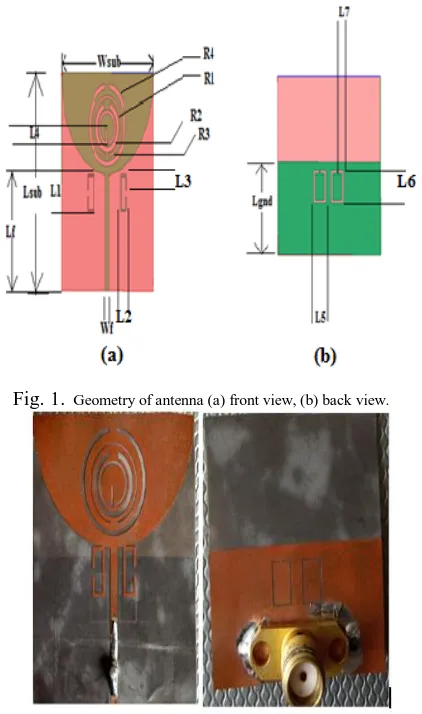
[image:2.595.306.519.50.244.2]The hexa-notched band antenna is designed by using ring resonators and defected ground structure. CSRR are used here which are placed on a semi circular patch, ring resonators are used and these are placed at the union of feedline, and a DGS is also used in the design. By using 20mil Rogers R04003 which is having a di-electric constant as 3.55 and a printed radiating patch is used. To yield six notches four CSRR are used along with SRR and DGS slots. The antenna proposed in this paper is having certain dimensions and they are listed below in Table 1. And the structure of the present antenna is represented in Fig. 1. Fig. 2 depicts the user model of the presented antenna.
Fig. 1. Geometry of antenna (a) front view, (b) back view.
Fig. 2. User model of hexa notched antenna.
TABLE I : Dimensions of Antenna
factor Value(mm) factor Value(mm)
Lsub 30 Lf 16.5
Wsub 28 L1 5
Lgnd 15.5 L2 2
Wf 1 L3 2
R1 4.25 R2 3.5
L4 2.4 L5 3.3
L6 5.3 L7 1.5
R3 2.5 R4 2.75
By using a formula stop band frequency corresponding to WIMAX (3.30-3.60GHz), lower WLAN (5.15-5.35GHz), upper WLAN (5.7-5.8GHz) are calculated as
(1)
(2)
is the relative permittivity of the substrate, c is speed of light; R is radius of ring resonator.
Whereas, the downlink of X-band (7.0-7.4GHz), uplink of X-band (8.1-8.5GHz) are approximately calculated by
(3)
Represents the guided wavelength, represents free space wavelength.
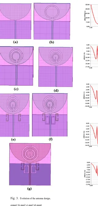
Evolution of antenna design:
[image:2.595.68.279.344.701.2]International Journal of Innovative Technology and Exploring Engineering (IJITEE) ISSN: 2278-3075, Volume-8 Issue-8, June 2019
Fig. 3. Evolution of the antenna design.
a)step1 b) step2 c) step3 d) step4
e) step5 f)step6 g)step7
Fig. 4. Simulation result of step1.
Fig. 5. Simulation result of step2.
Fig. 6. Simulation result of step3.
Fig. 7. Simulation result of step4.
Fig. 9. Simulation result of step6.
Fig. 10. Simulation result of step7.
III. SIMULATION RESULTS
The antenna is designed and simulated using HFSS software. Fabricated prototype of the designed antenna is also developed and it is mentioned in Fig (2). The antenna is simulated and obtained results are VSWR, return loss, radiation patterns, and antenna gain.
VSWR
[image:4.595.313.506.99.635.2]Hexa notched antenna is successfully rejecting six frequencies in which the first five frequency bands come under UWB technology and sixth frequency band is a J-band which is used for military appliances. The frequencies which are going to reject are WIMAX (3.3-3.5GHZ), lower WLAN (5.15-5.35GHZ), upper WLAN (5.7-5.8GHZ), downlink of X-band (6.8-7.4GHZ), uplink of X-band (7.6-8.10GHz), and J-band (11.2-12GHZ) bands. The shape can be altered and adjust position of central frequency and band width of each notched band. Measured and simulated results are shown below.
Fig. 11. Measured and Simulated VSWR of antenna. Radiation patterns
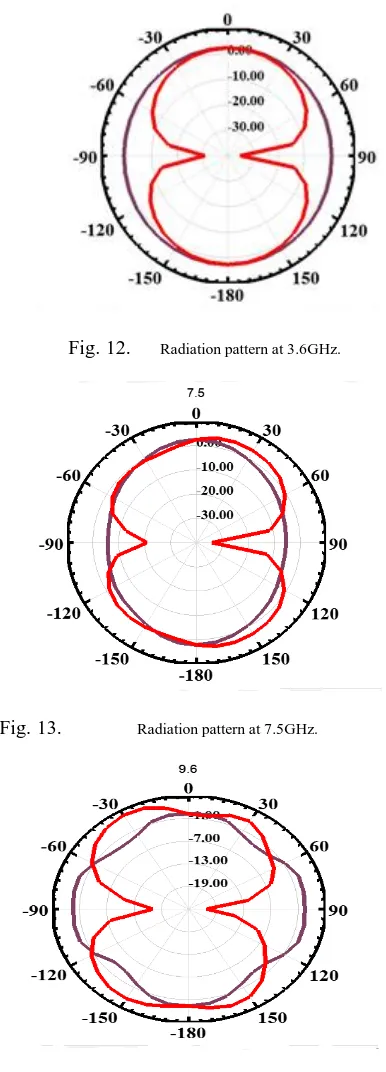
Radiation patterns are observed for the antenna. These radiation patterns are taken at pass band frequencies they are shown in following figures. The present antenna is having a radiation patterns which are omnidirectional and it is clearly shown that the antenna is almost having
dumbbell shaped design in E-plane. From this it can observed that the antenna is having radiation patterns which are having minimum band rejecting effect.
Fig. 12. Radiation pattern at 3.6GHz.
Fig. 13. Radiation pattern at 7.5GHz.
[image:4.595.61.275.174.286.2]
Fig. 14. Radiation pattern at 9.6GHz. Gain
[image:4.595.62.264.582.670.2]International Journal of Innovative Technology and Exploring Engineering (IJITEE) ISSN: 2278-3075, Volume-8 Issue-8, June 2019
Fig. 15. Gain of the proposed antenna.
parametric analyses of the notched frequency bands.
[image:5.595.313.519.77.165.2] [image:5.595.315.519.205.334.2]All the six notches of the present antenna can be controlled. The central frequency and bandwidth of the notched bands can be adjusted by altering the length and changing the radius of the ring resonators. The rejection bandwidth of WIMAX band can be altered by adjusting the radius of the R1 ring resonator. The result is mentioned in Fig.16. Lower WLAN is controlled by increasing or decreasing the radius of R2 ring resonator. It is mentioned in Fig.17.The behavior of upper WLAN is controlled by adjusting length L4 which is mentioned in Fig.18.Variations in downlink of X-band can be adjusted by SRR which are presented at left and right of feedline it is given in Fig.19. For shifting of uplink X-band parameter used is L3 in Fig.20.Then finally the variations in J-band are done by varying the parameter L1 it is admitted in Fig.21. The parametric analysis of frequency bands is done by using HFSS.
[image:5.595.315.523.371.493.2]Fig. 16.Mechanism for WIMAX frequency band.
Fig. 17.Mechanism for lower WLAN frequency band
[image:5.595.57.263.435.521.2]Fig. 18.Mechanism for upper WLAN frequency band
Fig. 19.Mechanism for downlink of X-band
Fig. 20.Mechanism for uplink of X-band.
Fig. 21.Mechanism for J-band.
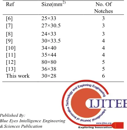
IV. COMPARISON
[image:5.595.62.264.561.647.2]By comparing some of the reference paper with our proposed work , it provides better idea about this design and it is shown in above Table .II.
TABLE II : Comparison of antenna with other structures.
Ref Size(mm2) No. Of
Notches
[6] 25×33 3
[7] 27×30.5 3
[8] 24×33 3
[9] 30×33.5 4
[10] 34×40 4
[11] 35×44 4
[12] 80×80 5
[13] 36×38 5
[image:5.595.323.544.607.833.2] [image:5.595.59.268.690.777.2]V. CONCLUSION
A compact hexa-notched band antenna is designed which rejects the following bands. WIMAX (3.3-3.6 GHz), lower WLAN (5.15-5.35GHZ), upper WLAN (5.7-5.8GHZ), downlink of X-band (7.0-7.4GHZ), uplink of X-band (8.1-8.5GHZ) and J-band (11.2-12GHZ).The six notches overcome the interference from narrow band devices operating in UWB and ,military devices(last band). For the proposed antenna all the notches can be controlled by varying suitable parameters. The antenna has an acceptable gain, VSWR and omnidirectional radiation patterns.
REFERENCES
1. Ahmed,O. and Sebak, A.R., “A printed monopole antenna with two steps and a circular slot for UWB applications,” IEEE Antennas and Wireless
Propagation Letters, 7, pp.411-413, IEEE, 2008.
2. Shameena, V.A., Mridula, S., Pradeep, A., Jacob, S., Lindo, A.O. and Mohanan, P., A compact CPW fed slot antenna for ultra wide band applications. AEU-International Journal of Electronics and
Communications, 66(3), pp.189-194, 2012.
3. Islam, M.T., Azim, R. and Mobashsher, A.T., Triple band-notched planar UWB antenna using parasitic strips. ProgressIn Electromagnetics
Research, 129, pp.161-179, 2012.
4. Lin, C.C., Jin, P. and Ziolkowski, R.W., Single, dual and tri-band-notched ultrawideband (UWB) antennas using capacitively loaded loop (CLL) resonators. IEEE Transactions on Antennas and Propagation, 60(1), pp.102-109, 2012.
5. Rani, M.S.A., Rahim, SK.., Kamarudin,M.., Peter, T., Cheung, S.W. and Saad, B.M., Electromagnetic behaviors of thin film CPW-fed CSRR loaded on UWB transparent antenna. IEEE Antennas and Wireless Propagation Letters, 13, pp.1239-1242, 2014.
6. Sung, Y., Triple band-notched UWB planar monopole antenna using a modified H-shaped resonator. IEEE Transactions on Antennas and
Propagation, 61(2), pp.953-957, 2013.
7. Cai,Y.Z., Yang, H.C. and Cai, L.Y., Wideband monopole antenna with three band-notched characteristics. IEEE Antennas and Wireless Propagation Letters, 13, pp.607-610, 2014.
8. Rahman, M., CPW fed miniaturized UWB tri-notch antenna with bandwidth enhancement. Advances in Electrical Engineering, 2016.
9. Jin, Y., Tak, J. and Choi, J., Quadruple band-notched trapezoid UWB antenna with reduced gains in notch bands. Journal of electromagnetic
engineering and science, 16(1), pp.35-43, 2016.
10.Sharma, M.M., Deegwal, J.K., Kumar, A. and Govil, M.C., Compact planar monopole UWB antenna with quadruple band-notched characteristics. Progress in Electromagnetics Research, 47, pp.29-36, 2014.
11.Li, T.Zhai, H., Li, G., Li, L. and LiangC., A compact ultra‐wideband antenna with four band‐notched characteristics. Microwave and Optical
Technology Letters, 54(12), pp.2862-2865, 2012.
12.Liu, J.J., Esselle, K.P., Hay, S.G. and Zhong, S.S., Planar ultra-wideband antenna with five notched stop bands. Electronics Letters, 49(9), pp.579-580, 2013.
13.Mewara, H.S., Deegwal, J.K. and Sharma, M.M., A slot resonators based quintuple band-notched Y-shaped planar monopole ultra-wideband antenna. AEU-Int Journal of Electronics and Communications, 83, pp.470-478, 2018.
M. Jyothi Pushpa, from Tadepalligudem, Andhra Pradesh, India. She received his B.Tech degree in the year 2017 from Sri Vasavi engineering college, Tadepalligudem (A.P), India. Currently he is pursuing M.Tech in CESP from VR Siddhartha engineering college, Vijayawada (A.P), India. His research interests are ULTRAWIDEBAND ANTENNAS and MIMO ANTENNAS.
A.Jhansi Rani, obtained her B.Tech Degree in Electronics and Communications Engineering from Velagapudi Ramakrishna Siddhartha Engineering College, Vijayawada in 1991 and M.Tech Degree in Microwave Engineering from Institute of Technology, Banaras Hindu University, and Varanasi in 1993. Later she joined as a Faculty in ECE Dept.,
of V.R.Siddhartha Engineering College, Vijayawada. She obtained Ph.D. Degree from JNTU, Hyderabad in August 2008. Presently, she is working as a Professor of ECE and PG -Programme Coordinator at V. R. Siddhartha Engineering College. Dr.Jhansi has more than 25 years of teaching experience, and has about 70 technical publications in various International and National Journals and Conferences to her credit. She is the Life Member of FIETE, MISTE, BMESI, and MSEMCEI. She received grants from DST, DLRL and AICTE in the area of Shared Aperture and smart Antennas. Her fields of interest include Electromagnetics, Smart Antennas, Analysis of Microwave Components, EM Waves and Transmission Lines, Numerical Methods and Applications.