This is a repository copy of
Direct Imaging of Kinetic Pathways of Atomic Diffusion in
Monolayer Molybdenum Disulfide
.
White Rose Research Online URL for this paper:
http://eprints.whiterose.ac.uk/117124/
Version: Published Version
Article:
Hong, Jinhua, Pan, Yuhao, Hu, Zhixin et al. (5 more authors) (2017) Direct Imaging of
Kinetic Pathways of Atomic Diffusion in Monolayer Molybdenum Disulfide. Nano Letters.
pp. 3383-3390. ISSN 1530-6984
https://doi.org/10.1021/acs.nanolett.6b05342
[email protected] https://eprints.whiterose.ac.uk/ Reuse
This article is distributed under the terms of the Creative Commons Attribution (CC BY) licence. This licence allows you to distribute, remix, tweak, and build upon the work, even commercially, as long as you credit the authors for the original work. More information and the full terms of the licence here:
https://creativecommons.org/licenses/
Takedown
If you consider content in White Rose Research Online to be in breach of UK law, please notify us by
Direct Imaging of Kinetic Pathways of Atomic Di
ff
usion in Monolayer
Molybdenum Disul
fi
de
Jinhua Hong,
†Yuhao Pan,
‡Zhixin Hu,
‡Danhui Lv,
†Chuanhong Jin,
*
,†Wei Ji,
*
,‡Jun Yuan,
*
,†,§and Ze Zhang
††
State Key Laboratory of Silicon Materials, School of Materials Science and Engineering, Zhejiang University, Hangzhou, Zhejiang 310027, China
‡
Beijing Key Laboratory of Optoelectronic Functional Materials and Micro-Nano Devices, Department of Physics, Renmin University of China, Beijing 100872, China
§
Department of Physics, University of York, Heslington, York YO10 5DD, United Kingdom
*
S Supporting InformationABSTRACT: Direct observation of atomic migration both on and below surfaces is a long-standing but important challenge in materials science as diffusion is one of the most elementary
processes essential to many vital material behaviors. Probing the kinetic pathways, including metastable or even transition states involved down to atomic scale, holds the key to the underlying physical mechanisms. Here, we applied aberration-corrected transmission electron microscopy (TEM) to demonstrate direct atomic-scale imaging and quasi-real-time tracking of diffusion of Mo adatoms and vacancies in
monolayer MoS2, an important two-dimensional transition
metal dichalcogenide (TMD) system. Preferred kinetic pathways and the migration potential-energy landscape are
determined experimentally and confirmed theoretically. The resulting three-dimensional knowledge of the atomic configuration
evolution reveals the different microscopic mechanisms responsible for the contrasting intrinsic diffusion rates for Mo adatoms
and vacancies. The new insight will benefit our understanding of material processes such as phase transformation and
heterogeneous catalysis.
KEYWORDS: Transition metal dichalcogenides, adatom and vacancy, surface migration, energy landscape, single-atom tracking
D
iffusion phenomena on surfaces and inside solids areimportant material processes closely associated with solid-state phase transformation,1 nanomaterials growth,2−4
single-atom doping,1and heterogeneous catalysis.5To tailor or design these diffusion-related properties,6 it is essential to
understand the underlying atomic process involved. However, the determination of microscopic mechanisms is nontrivial as diffusion can proceed along many different kinetic pathways.
Even for simple self-diffusion inside solids, for example, it can
take place via vacancy, interstitial or direct exchange mechanisms. Experimental determination of the stable and metastable configurations and their evolutions remains
important to identify the dominant kinetic pathways involved, as well as providing vital realistic calibration to the complex ab initio calculation.
Among the available experimental techniques, scanning tunneling microscopy (STM),7,8 atomic force microscopy (AFM),9 andfield ion microscopy (FIM)10have the required
atomic resolution to image the surface migration of adatoms,11−15 and the rotation,16 transformation9,17,18 and
self-assembly19of adsorbate molecules. With the development
of aberration correction optics, transmission electron micros-copy (TEM) has been demonstrated as an alternative technique with a proper time window to observe adatom diffusion20or
defect evolution.21−37 However, the experimental single-atom
tracking and statistical analysis of the metastable/intermediate states in atomic migration via different mechanisms are still
limited. Furthermore, in contrast with the well-known one-dimensional pathway-dependent barrier, the two-one-dimensional potential landscape of the surface diffusion has never been
mapped experimentally.
In this paper, we report a direct observation of the dynamics of bulk-like in-plane diffusion of Mo vacancies and surface
migration of Mo adatoms in monolayer MoS2, by atomic-scale
tracking using chemically sensitive scanning transmission electron microscopy (STEM). As monolayer MoS2 has a
sandwich structure consisting of a Mo layer bonded by surface S layers on both sides, it is an ideal model system to study and
Received: December 24, 2016 Revised: May 22, 2017 Published: May 26, 2017
Letter
pubs.acs.org/NanoLett
This is an open access article published under a Creative Commons Attribution (CC-BY)
contrast atom migration both on and below the surface. Specifically, we show that such observation can help identify the
preferred migration pathway and outline the two-dimensional migration energy landscape. Ab initio density function theory (DFT) calculation further provides detailed quantum mechan-ical description of the atomic processes along such kinetic pathways, accounting for the different diffusion rates measured
for adatoms and vacancies. As a member of transition metal dichalcogenides,38 MoS
2 has shown considerable potential in
applications such as catalysis39−43and electrode materials for
batteries.44,45 The insight gained can enhance our under-standing and optimization of applications of such materials and the relevant systems involving mass transport under either electronic, chemical, or ionic currents.
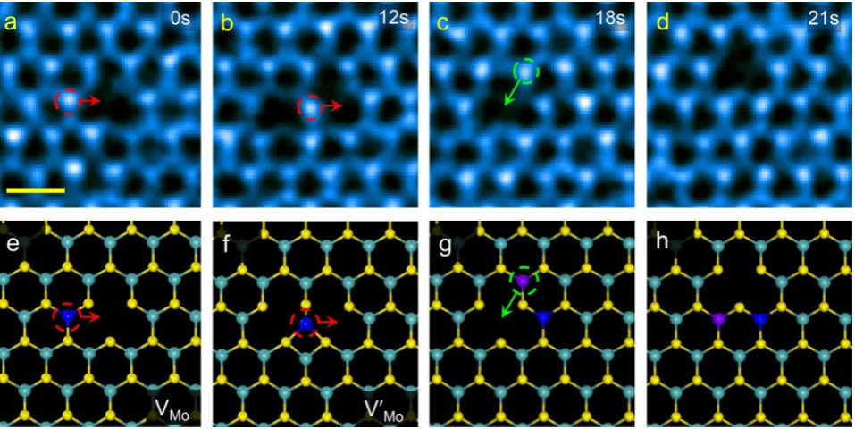
Results.The Migration of Mo Vacancy and Its Metastable State.Figure 1a−1d shows the time-lapsed annular dark-field
(ADF) images of the migrating Mo vacancy within monolayer MoS2 at room temperature. According to the Z-contrast
mechanism responsible for ADF-STEM imaging, it is easy to quantitatively assign the nature of lattice atoms and vacancy defects in monolayer MoS2. The total duration of observation
was sufficiently short that we did not detect additional loss of
Mo or S atoms in this area of interest. Note that the vacancy diffusion is actually the motion of the neighboring Mo atom,
highlighted with arrows in Figure 1a−1c. The vacancy
migration in Figure 1a−1c went through an intermediate
state (labeled asV′Mo) and gives the clue to the kinetic pathway for the hopping of Mo vacancy from one site in the Mo sublattice to the next (Figure 1d). More vacancy hopping examples can be found inSupporting Information Figures S1−
2andSI movie file 1,SI moviefile 2, andSI moviefile 3.
We have also analyzed the kinetic pathway of Mo vacancy migration by ab initio DFT calculation, starting with the atomic geometries deduced from TEM observation. Figure 1e−1h
show DFT fully relaxed atomic models associated withFigure 1a−1d in which the migrating Mo atom is emphasized in blue
and purple. The overall agreement between the experimental images and those derived from the DFT calculations confirms
the correct identification of three-dimensional structure of the
most stable vacancy configuration V
Mo (Figure 1a,1e) and
metastable stateV′Mo(Figure 1b,1f).
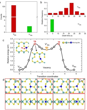
Figure 2a,2b shows the statistical counts and dwell-times of different configurations of Mo vacancy (VMo and V′Mo) observed during their migration. The dominating counts and longer dwell time of vacancies in the VMo state support the
proposition that it is the ground-state configuration whereas V′Mo is a metastable configuration. Our experimentally
determined kinetic pathway (Figure 1e−1g) for Mo vacancy
migration is consistent with the most-favored pathway derived from ab initio DFT calculation, after considering various possibilities, as shown in Figure 2c where the transition state (TS) and the energetics involved are also presented. The red arrows in Figure 2c indicate the motion of neighboring Mo atom (in blue) with the details shown inFigure 2d (see alsoSI moviefile 4). The TS state has an energy of 2.9 eV relative to
that of the most stable Mo vacancy state (VMo). The origin of
such a high energy barrier is the unsaturated Mo−S bonds and
reorganization of the bond length (Figure 2d). On the other hand, the energy of the metastable state V′Mo (local energy minimum in Figure 2c) is only 0.6 eV below that of the TS state, which explains the limited dwell time and observation frequency for the V′Mo state. This probably also explains the
slight distortion of lattice Mo atoms seen in the experimental images inFigure 1as the atomic configuration is more mobile
[image:3.625.75.554.68.308.2]in such a shallow potential well to be captured precisely. Nevertheless, both activation energies are higher than the background thermal energy, suggesting the migration processes seen inFigure 1is electron-beam assisted. This is similar to that found for vacancy hopping in graphene.31,46 Despite that, an analysis of the migration trajectories (Figure S3) indicates that the vacancy migration within Mo sublattice is without directional preference. The travel distance and displacement
Figure 1.Atomic-scale migration of vacancy defects. (a−d) Time-lapse series of experimental ADF images of a Mo vacancy. Scale bar: 0.5 nm. (e−h) DFT-relaxed atomic structures corresponding to the evolution in a−d from the Mo vacancy (VMoin a) to its metastable state (V′Moin b) and then to another Mo vacancyVMoin c. Scale bar: 0.5 nm. Note the vacancy migration is actually the motion of a neighboring Mo atom, shown in blue or purple.
Nano Letters Letter
of the Mo vacancy both follow the trend expected for the random walk motion (Figure S4). This suggests that the effect
of the electron beam is probably limited to boosting the mobilities of the atoms with high migration barriers.
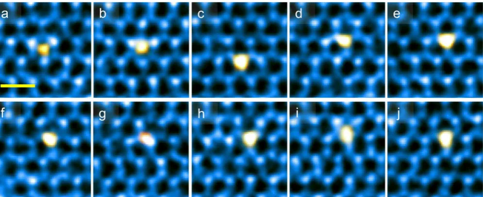
The Tracking of Mo Adatoms and Their Metastable States. For comparison, Figure 3a−3f show time-lapse
sequential ADF-STEM images indicating the migration of a Mo adatom on the surface of a monolayer MoS2. The Mo
adatom47 can be easily identified and this assignment is
supported by additional simulation and analysis shown in
Figures S5 and S6. More examples of adatom hopping are presented inFigure S7andSI moviefile 5,SI moviefile 6and SI moviefile 7.
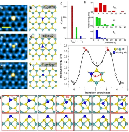
After analyzing numerous Mo adatoms (over 500 cases), we identified the following three most frequently observed
configurations of Mo adatoms: on top of Mo sites (TMo),
above the center of the hexagon or the hollow site (H), and on top of S sites (TS), shown inFigure 4a,4c,4e, respectively. The
corresponding atomic models are shown inFigure 4b,4d,4f, all based on the experimentally suggested geometry and fully relaxed by ab initio calculation. Side views of these structures are presented inFigure S8. The image simulations (Figure S9) based on these structural models are in agreement with the experiments.
The statistical analysis of the observed adsorption states in
Figure 4g demonstrates that TMois the most common adatom
configuration, and H and TSare less common by comparison.
Correspondingly, the dwell time of adatoms shown inFigure 4h also indicates that TMo is more stable than H and TS,
although the differences in the counting statistics and the dwell
times among TMo, H, and TSare smaller than those found in
[image:4.625.136.497.64.519.2]the case of Mo vacancy. Consistent with the experimental
Figure 2.States of vacancy and their evolution. (a,b) Statistical counts and dwell time of vacancies and their metastable states during the migration of a Mo vacancy. (c) DFT calculated migration pathway of Mo vacancy. The dynamic process is shown by the inset atomic models with arrows illustrating the migration pathway of the neighboring Mo atom. (d) Detailed atomic dynamics of Mo vacancy migration with top-view and side-view, respectively. Note theVMo→V′Mo→VMotransition in c is symmetric, hence only thefirst half process of vacancy migration (right red arrow in c) is drawn detailed in d. Also note the top-view of the top-row structures in d is rotated with respect to the structures in c and that inFigure 1.
result, DFT calculations give their relative energy as 0, 0.33, and 0.99 eV for TMo, H, and TS, respectively. Accordingly, we regard
TMoas the most stable state and H, TSas metastable states. The
presence of more than one metastable state for adatom migration is a reflection of the increased degree of freedom of
adatoms compared with that of the in-plane vacancy diffusion.
This illustrates the richness of the surface diffusional
phenomena and necessity of determining the dominant kinetic pathway.
Ab initio calculation confirms that the experimentally
most-favored kinetic pathway for Mo adatom migration follows a TMo1→H→TMo2transition (red arrows shown inFigure 4i
and observed inSI moviefile 5) with an initial energy barrier of
0.62 eV. The energy barrier for the less-favored TMo → TS
transition is calculated to be 1.11 eV by comparison (Figure S10 and SI movie file 8). The detailed structure evolution
across the TMo1 → H → TMo2 transition can be followed in Figure 4j where the migrating adatom is emphasized in blue (see also SI movie file 9). Compared with Mo vacancy
diffusion, the reduced energy barriers for surface adatom
migration are related to the smaller structural relaxation (Figure S11) with breaking of at most only one Mo−S bond.
Although both MoS2and graphene surfaces are considered to
be inert, the kinetic pathways for the adatoms are very different
and depend on both the surface and the adatoms, indicating strong chemical adatom−surface interaction in both cases. For
example, adatoms on graphite still migrate in a similar hexagonal lattice but they follow either T1 → B → T2 (Au
adatom), H1→B→H2(Al or Cr) or B1→B2(C adatom)
pathways.24,48Here B stands for bridge sites above the center of CC bonds. By contrast, the bridge-site adsorption on MoS2
is not, even locally, a stable configuration for Mo adatoms. The
preference for the TMo1→H→TMo2pathway on MoS2surface
is, we believe, due to the tendency of thed-electrons of the Mo adatom to form covalent bonds with the surface S in a triangular-prismatic or octahedral coordination.49This
chemi-cally sensitive adatom diffusion may dominate the diffusion of
intercalating ions in layered materials as battery electrodes.41 Similar to the Mo vacancy case, the migration trajectory of Mo adatoms suggests that the migration jumps have no obvious directional preference (Figure S12). The travel distance and
displacement of the hopping Mo adatom (Figure S4) is typical of random walk or Brownian motion, suggesting the electron beam may help overcome the migration energy barriers.
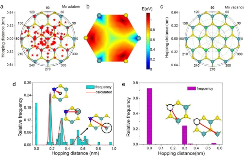
Hopping Statistics of Defect Migration and Potential Energy Landscape.The Mo adatom hopping statistics can be visualized spatially in terms of the polar scatter diagram shown inFigure 5a. The red star dots indicate thefinal sites of
one-step adatom hopping from the initial site on Mo (coordinate origin), all superimposed on the hexagonal MoS2lattice. The
radii of inscribed circles represent the range of the hopping steps that can be reached from the circle’s center. Most hoppings are between TMo and H, without directional
preference. The density distribution of dots in this polar diagram reflects the two-dimensional potential landscape of a
Mo adatom on monolayer MoS2, as higher density means more
stable atomic configuration. The density distribution indeed
coincides qualitatively with the theoretical adsorption potential diagram shown inFigure 5b. The TMo, H, and TSsites are all
valleys in this potential-energy landscape, corresponding to the ground and metastable states, shown inFigure 4, respectively. The contrasting energy barriers between TMo →H (0.62 eV)
and TMo→TS(1.11 eV) indicate that the TMo→H transition
should be the elementary hopping process in thermally activated atomic migration.
Similarly, polar scatter diagram inFigure 5c summarizes the hopping step distribution of Mo vacancies, where green triangles stand for the final sites of one-step hopping of Mo
vacancy whose initial site is the origin. Compared with the surface adatom migration, the energy landscape is much simpler asVMojumps only between Mo sublattice sites. Moreover, this stable migration within the Mo layer also has no directional preference, indicating a 2D random walk behavior.
One should note that as individual one-step migration of defects occurs in picosecond, the transfer process itself is too fast to capture“inflight”. The possible much longer dwelling on
the ground- or metastable-state sites allows us to capture different ground/metastable configurations. Hence, we consider
the observed transition between two different states as one
[image:5.625.66.564.67.270.2]hopping step, much slower than the “ps” hopping dynamics. On the basis of the above analysis of the potential landscape for Mo adatoms, we interpret the observed long-range one-step
Figure 3.Atomic migration of Mo adatom defects. (a−j) Experimental time sequential of ADF images of Mo adatom hopping as an example. Time interval: 3 s. Scale bar: 0.5 nm. Different false colors are used for better visualization.
Nano Letters Letter
jumps in Figure 5a as consisting of several TMo → H
elementary hopping events. This is supported by the relative population of the jumping steps as shown inFigure 5d, based on an independent hopping model. Here the “zero peak”
represents those observations that adatoms remain at the same site or return to the same starting site. Thefirst peak around
0.18 nm represents the transition from TMo to H (the
elementary hopping), and the second peak is attributed to transition from TMo1to TMo2 (two successive basic hopping),
and the third peak is the result of second-nearest-neighboring hopping, as illustrated by the insets in Figure 5d. They are compared with the theoretically predicted relative probability distribution, where the relative probability ratio of the elementary hopping TMo → H, nearest-neighboring-site
hopping TMo1→H →TMo2 and
second-nearest-neighboring-site hopping is 1:2/3:1/6 (red curve, seeFigure S13 and Note 1
for details). The calculated results agree well with the experiment except the discrepancy for peak 3 at 0.64 nm due to the limited counts for long-range jumps and the possible involvement of the less-favored TMo →TSpathway.
Figure 5e shows the hopping step of Mo vacancy. The vacancy has a much lower possibility to migrate in comparison with the case of adatom hopping, due to its much higher energy barrier. Nearest-neighboring vacancy hopping is responsible for the first peak and the second-nearest neighboring hopping
contributes to the second peak (see inset pictures).
Discussion. For adatom surface migration, the structural evolution give rise to novel electronic properties, worth exploring by DFT calculation. We discover that certain adatom configurations (ground state T
Mo and metastable state H, TS)
all have magnetic moments >2μB(Figure S14). They are all
[image:6.625.105.523.66.495.2]highly spin-polarized and localized mainly on Mo adatom with
Figure 4.Adsorption states and their evolution along the kinetic pathway. (a−f) Atomically resolved ADF images and structure models of different adsorption states on top of Mo site (TMo), at hexagon-center or hollow site (H), and on top of S site (TS), respectively. Scale bar: 0.5 nm. False color is used to better illustrate the adatom configuration. Relative energies of different adatom states are given. (g) Statistical counts of different
adsorption states in a,c,e. (h) Statistical dwell time of different adatom structures. (i) DFT revealed energetics and pathway for evolution between
ground state TMo, transition state TS, and metastable state H. (j) Detailed atomic dynamics of transition from TMoto H with top view and side view of the three-dimensional atomic structure, respectively. Note the TMo1→H→TMo2transition in i is symmetric, hence only thefirst half process (left
red arrows in i) is drawn.
a minor contribution from the neighboring S atoms. The significant density of states (mostly from the adatom’s d
orbitals) at Fermi levels may play an essential role in the physical properties of MoS2, such as defect magnetism and
reactivity as a catalyst.
The very different magnitudes of the energy barriers for Mo
adatoms and vacancies can be ascribed to their contrasting microscopic diffusion mechanisms. In surface diffusion,
adatoms not only relax more easily into the vacuum but also retain the largest number of unbroken Mo−S bonds. A Mo
adatom starts with three Mo−S bonds in the
triangular-prismatic coordination as the most stable state49at TMosite to
two Mo−S bonds when going through a S−S bridge site, then
to three Mo−S bonds in octahedral coordination49(H site),
which is less energetically favorable. In the vacancy diffusion,
Mo’s migration within the confined Mo atom layer involves the
breaking and reconnection of more covalent Mo−S bonds
(Figure 2d): from initial Mo site (most stable with six Mo−S
bonds), through a S−S bridge site (two short Mo−S bonds
with the“Klein”-like S atoms, two long and weak Mo−S bonds
with the “zigzag”-like S atoms, Figure S11b), to a hollow-like site (metastable with six Mo−S bonds).
Finally, the observation of vacancy hopping and metastable adatom TSwith energy barriers much higher than the thermal
energy available is a sign that the migration is influenced or
even driven by the electron beam. Hence it is necessary to quantify the beam induced effect. Considering elastic knock-on
scattering mechanism (Figures S15 and S16), we conclude that the vacancy migration is induced solely by the electron beam and adatom migration is influenced by both thermal activation
and beam-atom interaction. Fortunately, the beam-atom interaction allows us to explore more comprehensively different
kinetic pathways, especially for vacancy dynamics inaccessible by thermal activation at a “safe” temperature. One may also note the slight atomic distortion of the lattice Mo below the migrating Mo in the vacancy hopping inFigure 1, which can be interpreted as a temporary displacement resulting from the electron beam radiation on the shallow potential landscape shown above. In the future studies, it would be very interesting to carry out in situ TEM observation at variable temperatures and with higher temporal resolution, which would allow us to capture more precisely the atomic dynamics and determine quantitatively the migration kinetics experimentally, as a complement to DFT calculations.
In summary, we have demonstrated an efficient survey of the
migration energy landscape using single-atom tracking and ab initio calculation, providing a successful paradigm for exploration of the microscopic mechanisms of atom diffusion
in solids. Its application in monolayer MoS2reveals the
two-dimensional Mo diffusions on and below surface with very
different covalent bonds reorganization along their preferred
[image:7.625.60.564.60.383.2]kinetic pathway. The results from our joint experiment-theory approach should be useful in the rational design of practical applications of TMDs, such as catalysts and ion intercalation in
Figure 5.Statistical hopping steps of adatom and vacancy defects. (a) Polar scatter diagram of hopping steps from the coordinate origin where Mo lattice locates. Red star dots indicate thefinal position of adatom hopping from the initial state at the origin. The data is obtained from analyzing over
50 time series of ADF images of adatom defects on MoS2monolayers, (b) DFT calculated two-dimensional potential diagram for a Mo adatom on the hexagonal MoS2lattice. TMosites and hexagon center H site are potential valleys. (c) Polar scatter diagram showing hopping steps of Mo vacancy from the origin. (d) Hopping step statistics of Mo adatom migration. Insets show the corresponding atomic hopping models which are supported by the calculated probability distribution. (e) Hopping step distribution of Mo vacancy with inset models presenting the migration process.
Nano Letters Letter
electrodes for batteries, as well as bringing us a new perspective on solid state mass transport in general.
During the review of this work, we noticed another work focused on the migration of single Pt atoms in MoS2
monolayer.56
Methods. Sample Preparation. Monolayer molybdenum disulfide was prepared onto silicon substrate with a 300 nm
thick oxide capping layer through standard mechanical exfoliation from bulky MoS2 single crystals (SPI Supplies
Inc.) using scotch tapes. Selected atomically thin samples were then transferred onto TEM grids and annealed at 200 °C in
vacuum (10−4 Pa) to remove surface residues and
contami-nations before loading into the TEM chamber.
ADF-STEM Characterization. ADF-STEM imaging was carried out in a FEI Titan ChemiSTEM microscope equipped with a probe corrector and operated at 200 kV. The probe current was set to be about 60 pA and the convergence angle to 22 mrad. The collection angle of the ADF-STEM detector was adjusted to 50−200 mrad. Time lapsed ADF-STEM images
were recorded in three seconds interval with a frame size of 512
×512 pixels (corresponding to 10×10 nm2) and a pixel dwell
time of 10μs. The total electron dose to the specimen for each
frame was estimated to be 9.7 × 10⁶ e−/nm2. ADF-STEM
images were analyzed after a drift correction and Wiener
filtering for a better signal-to-noise (S/N) ratio (Figure S17).
All the observations were carried out at room temperature. ADF-STEM image simulations, as shown in the Figure S9, were achieved by QSTEM50 with the simulation parameters (the convergence and acceptance angles, the probe size) kept almost the same as those used experimentally.
Further analysis including the population, the duration time (or lifetime), and hopping step statistics were performed based on the raw ADF-STEM images recorded from clean regions of MoS2monolayers.
DFT Calculations. Density functional theory calculations were performed using the generalized gradient approximation for the exchange-correlation potential, the projector augmented wave method51and a plane-wave basis set as implemented in
the Vienna ab initio simulation package (VASP).52The energy cutofffor plane wave was set to 300 eV for structural relaxation
and increased to 600 eV for total energy calculations. Dispersion correction was made at the van der Waals density functional (vdW-DF) level, with the optB86b functional for the exchange potential.53An 8×8 slab of monolayer MoS2with a
15 Å vacuum layer perpendicular to the atomic plane was employed in all calculations to minimize the interactions between a defect and its images. All atoms in the supercell were allowed to relax until the residual force per atom was less than 0.01 eV·Å−1. Barriers of different diffusion pathways were
revealed by the nudged elastic band (NEB) method.54 The climbing-image technique55 was used to precisely identify the transition state and the barrier height.
Potential Landscape.The two-dimensional potential land-scape of the adatom was calculated as follows. Wefirst mapped
25 adsorption sites onto one-third of the lattice hexagon with equal spacing in the atomic plane (xyplane). A Mo adatom was put at these sites with its x-, y-coordinates fixed and z
-coordinates free to relax. Given the minimum energies at those sites, we extrapolate the energies into the whole hexagon to yield a continuous two-dimensional projected potential.
■
ASSOCIATED CONTENT*
S Supporting InformationThe Supporting Information is available free of charge on the
ACS Publications website at DOI: 10.1021/acs.nano-lett.6b05342.
Supplementary Figures 1−19 and Notes 1 and 2 (PDF)
Movie 1 (AVI) Movie 2 (AVI) Movie 3 (AVI) Movie 4 (AVI) Movie 5 (AVI) Movie 6 (AVI) Movie 7 (AVI) Movie 8 (AVI) Movie 9 (AVI)
■
AUTHOR INFORMATIONCorresponding Authors
*E-mail: (C.J.)[email protected]. *E-mail: (W.J.)[email protected].
*E-mail: (J.Y.) [email protected]. ORCID
Jinhua Hong:0000-0002-6406-1780
Author Contributions
J.H. and Y.P. contributed equally to this work. C.J., W.J., and J.Y. conceived the research. J.H. and D.L. contributed to the sample preparations. J.H., C.J., and J.Y. performed the STEM characterizations, data analysis and image simulations. Y.P., Z.H., and W.J. performed the DFT calculations. All authors discussed the results and contributed to the preparation of the manuscript.
Notes
The authors declare no competingfinancial interest.
■
ACKNOWLEDGMENTSThis work wasfinancially supported by the National Science
Foundation of China under Grants 51472215, 51222202, 91433103, 11274380, 11622437, and 61674171, the National Basic Research Program of China under Grants 2014CB932500 and 2015CB921004, the 111 project under Grant B16042, and the Fundamental Research Funds for the Central Universities and the Research Funds of Renmin University of China under Grant 16XNLQ01. The work on electron microscopy was done at the Center of Electron Microscopy of Zhejiang University. Calculations were performed at the Physics Lab of High-Performance Computing of Renmin University of China and Shanghai Supercomputer Center. We acknowledge Dr. Fang Lin for her assistance on Wienerfiltering. J.Y. acknowledged the
Pao Yukung International Foundation for the Chair Professor-ship in Zhejiang University, and thefinancial support from the
EPSRC (U.K.) funding EP/G070326 and EP/J022098. We also acknowledge Professor Ray F. Egerton for careful reading of this paper and useful suggestions.
■
REFERENCES(1) Lin, Y. C.; Dumcenco, D. O.; Huang, Y. S.; Suenaga, K.Nat. Nanotechnol.2014,9, 391−396.
(2) Hannon, J. B.; Kodambaka, S.; Ross, F. M.; Tromp, R. M.Nature
2006,440, 69−71.
(3) Hofmann, S.; Csanyi, G.; Ferrari, A. C.; Payne, M. C.; Robertson, J.Phys. Rev. Lett.2005,95, 036101.
(4) Jensen, L. E.; Bjork, M. T.; Jeppesen, S.; Persson, A. I.; Ohlsson, B. J.; Samuelson, L.Nano Lett.2004,4, 1961−1964.
(5) Satterfield, C. N.Mass transfer in heterogeneous catalysis; The MIT
Press, 1970.
(6) Mantina, M.; Wang, Y.; Arroyave, R.; Chen, L. Q.; Liu, Z. K.; Wolverton, C.Phys. Rev. Lett.2008,100, 215901.
(7) Bollinger, M. V.; Lauritsen, J. V.; Jacobsen, K. W.; Norskov, J. K.; Helveg, S.; Besenbacher, F.Phys. Rev. Lett.2001,87, 196803.
(8) Kibsgaard, J.; Lauritsen, J. V.; Laegsgaard, E.; Clausen, B. S.; Topsoe, H.; Besenbacher, F.J. Am. Chem. Soc. 2006,128, 13950− 13958.
(9) de Oteyza, D. G.; Gorman, P.; Chen, Y. C.; Wickenburg, S.; Riss, A.; Mowbray, D. J.; Etkin, G.; Pedramrazi, Z.; Tsai, H. Z.; Rubio, A.; Crommie, M. F.; Fischer, F. R.Science2013,340, 1434−1437.
(10) Tsong, T. T.Phys. Today1993,46, 24−31.
(11) Pedersen, M. O.; Osterlund, L.; Mortensen, J. J.; Mavrikakis, M.; Hansen, L. B.; Stensgaard, I.; Laegsgaard, E.; Norskov, J. K.; Besenbacher, F.Phys. Rev. Lett.2000,84, 4898−4901.
(12) Schaub, R.; Wahlstrom, E.; Ronnau, A.; Laegsgaard, E.; Stensgaard, I.; Besenbacher, F.Science2003,299, 377−379.
(13) Lo, R. L.; Hwang, I. S.; Ho, M. S.; Tsong, T. T.Phys. Rev. Lett.
1998,80, 5584−5587.
(14) Brune, H.; Wintterlin, J.; Behm, R. J.; Ertl, G.Phys. Rev. Lett.
1992,68, 624−626.
(15) Wang, K. D.; Zhang, C.; Loy, M. M. T.; Xiao, X. D.Phys. Rev. Lett.2005,94, 036103.
(16) Gao, L.; Liu, Q.; Zhang, Y. Y.; Jiang, N.; Zhang, H. G.; Cheng, Z. H.; Qiu, W. F.; Du, S. X.; Liu, Y. Q.; Hofer, W. A.; Gao, H. J.Phys. Rev. Lett.2008,101, 197209.
(17) Shi, D. X.; Ji, W.; Yang, B.; Cun, H. Y.; Du, S. X.; Chi, L. F.; Fuchs, H.; Hofer, W. A.; Gao, H. J. J. Phys. Chem. C 2009, 113, 17643−17647.
(18) Cheng, F.; Ji, W.; Leung, L.; Ning, Z. Y.; Polanyi, J. C.; Wang, C. G.ACS Nano2014,8, 8669−8675.
(19) Maksymovych, P.; Sorescu, D. C.; Yates, J. T.Phys. Rev. Lett.
2006,97, 146103.
(20) Lin, Y. C.; Dumcenco, D. O.; Komsa, H. P.; Niimi, Y.; Krasheninnikov, A. V.; Huang, Y. S.; Suenaga, K.Adv. Mater.2014,26, 2857−2861.
(21) Komsa, H.-P.; Kurasch, S.; Lehtinen, O.; Kaiser, U.; Krasheninnikov, A. V. Phys. Rev. B: Condens. Matter Mater. Phys.
2013,88, 035301. Oh, S. H.; Benthem, K. v.; Molina, S. I.; Borisevich, A. Y.; Luo, W.; Werner, P.; Zakharov, N. D.; Kumar, D.; Pantelides, S. T.; Pennycook, S. J.Nano Lett.2008,8, 1016−1019.
(22) Lehtinen, O.; Kurasch, S.; Krasheninnikov, A. V.; Kaiser, U.Nat. Commun.2013,4, 2098.
(23) Lee, J.; Zhou, W.; Pennycook, S. J.; Idrobo, J. C.; Pantelides, S. T.Nat. Commun.2013,4, 1650.
(24) Lehtinen, P. O.; Foster, A. S.; Ayuela, A.; Krasheninnikov, A.; Nordlund, K.; Nieminen, R. M.Phys. Rev. Lett.2003,91, 017202.
(25) Kurasch, S.; Kotakoski, J.; Lehtinen, O.; Skakalova, V.; Smet, J.; Krill, C. E.; Krasheninnikov, A. V.; Kaiser, U.Nano Lett. 2012,12, 3168−3173.
(26) Gan, Y. J.; Sun, L. T.; Banhart, F.Small2008,4, 587−591. Girit, Ç. Ö.; Meyer, J. C.; Erni, R.; Rossell, M. D.; Kisielowski, C.; Yang, L.;
Park, C.-H.; Crommie, M.; Cohen, M. L.; Louie, S. G.Science2009,
323, 1705−1708.
(27) Zhang, W.; Sun, L. T.; Xu, Z. J.; Krasheninnikov, A. V.; Huai, P.; Zhu, Z. Y.; Banhart, F.Phys. Rev. B: Condens. Matter Mater. Phys.2010,
81, 125425.
(28) Cretu, O.; Krasheninnikov, A. V.; Rodriguez-Manzo, J. A.; Sun, L. T.; Nieminen, R. M.; Banhart, F.Phys. Rev. Lett.2010,105, 196102. (29) Nakada, K.; Ishii, A.Solid State Commun.2011,151, 13−16. (30) Krasheninnikov, A. V.; Nordlund, K.; Lehtinen, P. O.; Foster, A. S.; Ayuela, A.; Nieminen, R. M.Phys. Rev. B: Condens. Matter Mater. Phys.2004,69, 073402.
(31) Kotakoski, J.; Mangler, C.; Meyer, J. C.Nat. Commun.2014,5, 3991.
(32) Robertson, A. W.; Allen, C. S.; Wu, Y. A.; He, K.; Olivier, J.; Neethling, J.; Kirkland, A. I.; Warner, J. H.Nat. Commun.2012, 3, 1144.
(33) Wang, W. L.; Santos, E. J. G.; Jiang, B.; Cubuk, E. D.; Ophus, C.; Centeno, A.; Pesquera, A.; Zurutuza, A.; Ciston, J.; Westervelt, R.; Kaxiras, E.Nano Lett.2014,14, 450−455.
(34) Warner, J. H.; Margine, E. R.; Mukai, M.; Robertson, A. W.; Giustino, F.; Kirkland, A. I.Science2012,337, 209−212.
(35) Ishikawa, R.; Mishra, R.; Lupini, A. R.; Findlay, S. D.; Taniguchi, T.; Pantelides, S. T.; Pennycook, S. J. Phys. Rev. Lett. 2014, 113, 155501.
(36) Lin, J.; Pantelides, S. T.; Zhou, W.ACS Nano2015,9, 5189− 5197.
(37) Wang, S.; Lee, G.-D.; Lee, S.; Yoon, E.; Warner, J. H.ACS Nano
2016,10, 5419−5430.
(38) Wang, Q. H.; Kalantar-Zadeh, K.; Kis, A.; Coleman, J. N.; Strano, M. S.Nat. Nanotechnol.2012,7, 699−712.
(39) Norskov, J. K.; Bligaard, T.; Rossmeisl, J.; Christensen, C. H.
Nat. Chem.2009,1, 37−46.
(40) Hinnemann, B.; Moses, P. G.; Bonde, J.; Jorgensen, K. P.; Nielsen, J. H.; Horch, S.; Chorkendorff, I.; Norskov, J. K.J. Am. Chem. Soc.2005,127, 5308−5309.
(41) Gao, M. R.; Liang, J. X.; Zheng, Y. R.; Xu, Y. F.; Jiang, J.; Gao, Q.; Li, J.; Yu, S. H.Nat. Commun.2015,6, 5982.
(42) Sun, X.; Dai, J.; Guo, Y. Q.; Wu, C. Z.; Hu, F. T.; Zhao, J. Y.; Zeng, X. C.; Xie, Y.Nanoscale2014,6, 8359−8367.
(43) Xie, J. F.; Zhang, H.; Li, S.; Wang, R. X.; Sun, X.; Zhou, M.; Zhou, J. F.; Lou, X. W.; Xie, Y.Adv. Mater.2013,25, 5807.
(44) Liu, H.; Su, D. W.; Zhou, R. F.; Sun, B.; Wang, G. X.; Qiao, S. Z.
Adv. Energy Mater.2012,2, 970−975.
(45) Li, W. F.; Yang, Y. M.; Zhang, G.; Zhang, Y. W.Nano Lett.2015,
15, 1691−1697.
(46) Lee, G. D.; Wang, C. Z.; Yoon, E.; Hwang, N. M.; Kim, D. Y.; Ho, K. M.Phys. Rev. Lett.2005,95, 205501.
(47) Zhou, W.; Zou, X. L.; Najmaei, S.; Liu, Z.; Shi, Y. M.; Kong, J.; Lou, J.; Ajayan, P. M.; Yakobson, B. I.; Idrobo, J. C.Nano Lett.2013,
13, 2615−2622.
(48) Hardcastle, T. P.; Seabourne, C. R.; Zan, R.; Brydson, R. M. D.; Bangert, U.; Ramasse, Q. M.; Novoselov, K. S.; Scott, A. J.Phys. Rev. B: Condens. Matter Mater. Phys.2013,87, 195430.
(49) Chhowalla, M.; Shin, H. S.; Eda, G.; Li, L. J.; Loh, K. P.; Zhang, H.Nat. Chem.2013,5, 263−275.
(50) Koch, C. T. QSTEM (2010). Determination of core structure periodicity and point defect density along dislocations. Ph.D Thesis, Arizona State University, Tempe, AZ, 2002.
(51) Blochl, P. E.Phys. Rev. B: Condens. Matter Mater. Phys.1994,50, 17953−17979.
(52) Kresse, G.; Furthmuller, J.Phys. Rev. B: Condens. Matter Mater. Phys.1996,54, 11169−11186.
(53) Klimes, J.; Bowler, D. R.; Michaelides, A.Phys. Rev. B: Condens. Matter Mater. Phys.2011,83, 195131.
(54) Henkelman, G.; Jonsson, H.J. Chem. Phys.2000,113, 9978− 9985.
(55) Henkelman, G.; Uberuaga, B. P.; Jonsson, H.J. Chem. Phys.
2000,113, 9901−9904.
(56) Li, H.; Wang, S.; Sawada, H.; Han, G. G.; Samuels, T.; Allen, C. S.; Kirkland, A. I.; Grossman, J. C.; Warner, J. H.ACS Nano2017,11, 3392−3403.
Nano Letters Letter