This is a repository copy of High-Mobility Toolkit for Quantum Dot Films. White Rose Research Online URL for this paper:
http://eprints.whiterose.ac.uk/107605/ Version: Accepted Version
Article:
Gómez-Campos, FM, Rodríguez-Bolívar, S and Califano, M (2016) High-Mobility Toolkit for Quantum Dot Films. ACS Photonics, 3 (11). pp. 2059-2067. ISSN 2330-4022
https://doi.org/10.1021/acsphotonics.6b00377
Reuse
Unless indicated otherwise, fulltext items are protected by copyright with all rights reserved. The copyright exception in section 29 of the Copyright, Designs and Patents Act 1988 allows the making of a single copy solely for the purpose of non-commercial research or private study within the limits of fair dealing. The publisher or other rights-holder may allow further reproduction and re-use of this version - refer to the White Rose Research Online record for this item. Where records identify the publisher as the copyright holder, users can verify any specific terms of use on the publisher’s website.
Takedown
If you consider content in White Rose Research Online to be in breach of UK law, please notify us by
High-mobility toolkit for quantum dot films
Francisco M. Gómez-Campos,
†,‡Salvador Rodríguez-Bolívar,
†,‡and Marco
Califano
∗,¶Departamento de Electrónica y Tecnología de Computadores, Facultad de Ciencias, Universidad de Granada, 18071 Granada, Spain , CITIC-UGR, C/ Periodista Rafael Gómez Montero, n 2, Granada, Spain , and Institute of Microwaves and Photonics, School of Electronic and Electrical
Engineering, University of Leeds, Leeds LS2 9JT, United Kingdom
E-mail: [email protected]
∗To whom correspondence should be addressed
Graphical TOC Entry
PbSe wzCdSe InAs zbCdSe InSb
mobility
effective mass
inter-dot coupling
miniband width
Abstract
Semiconductor colloidal quantum dots (CQDs) are being increasingly exploited
in electronics, optoelectronics and solar energy harvesting, using a variety of
differ-ent architectures, mostly based on ordered 2D or 3D arrays of these nanostructures.
A crucial issue for optimising the performance of such devices is the ability to
pre-dict and tune the transport properties of these assemblies. In this work we provide
general guidelines to precisely that effect, indicating specific materials, crystal
struc-tures, lattice arrangements, surface stoichiometries and morphologies which favour
high electron mobilities in these systems, and, conversely, materials that will exhibit
low mobilities if nanostructured. At the same time our results evidence a
surpris-ing independence of the film’s transport properties from those of the bulk material
from which the dots are made, highlighting the crucial role of theoretical modelling
to guide device design.
Keywords: transport, nanocrystal quantum dots, films, dot arrays, pseudopotential
method
Colloidal quantum dots (CQDs) are attractive material systems characterized by
out-standing properties, such as low manufacturing costs, high degree of uniformity and
flex-ibility achieved in their synthesis, size-tunability of their electronic and optical properties,
and even the ability to engineer their wave functions, enabling unprecedented control
of the carriers’ localization, that make them potentially ideally suited for a wide range
of technological applications. Nevertheless the performance of CQD-based electronic
and optoelectronic devices is still far from optimal, owing mainly to the poor transport
properties displayed by their building blocks when arranged in arrays. The presence
of countless interfaces, with associated traps1 and potential steps, that the charge
carri-ers need to cross in order to reach the electrodes where they can be collected, appears a
daunting obstacle to efficient transport in these devices. Indeed measurements on early
devices seemed to confirm this bleak scenario, and very low mobilities (of the order of
various theoretical models that predicted transport to occur through inefficient
phonon-assisted (or ’hopping’) conduction6–10 or direct tunnelling,2–4,11 leading to poor carrier
mobility in these systems. Nevertheless surprisingly high mobilities were reported lately
by several groups,12–18in high quality films made of different materials, suggesting that
band-like transport through extended states is indeed achievable in CQD arrays,
pro-vided the surface traps are effectively passivated18–25and the separation between dots is
reduced sufficiently by the use of extremely short ligands or inorganic capping.26This
hy-pothesis is supported by the observed temperature dependence of mobility and
conduc-tivity12–18whereas the spectral broadening and red shifts of the 1S exciton peak observed
in these systems,13,27may be indicative of strong electronic coupling between QDs, as are
the remarkable values of diffusion lengths and lifetimes of charge carriers measured in
QD solids.28
In this work, we carried out a comprehensive and systematic study of the electronic
structure and transport properties of CQD films made of different semiconductor
mate-rials, representatives of groups III-V, II-VI, and IV-VI, having different bulk crystal
struc-tures, varying from zinc blende to wurtzite to rocksalt, considering building blocks (dots)
of different sizes, surface morphologies and stoichiometries, placed at different distances
from each other and ordered according to different lattice types.
Our results evidence a surprising independence of the film’s transport properties from
those of the bulk material from which the dots are made, and indicate a strong influence of
the dot’s structural characteristics (crystal structure, stoichiometry and surface
morphol-ogy) on the resulting film mobilities. These findings provide invaluable general
guide-lines to engineer the electron mobility in these systems. Finally, our calculated electron
mobilities for CQD films of different materials are consistent with those recently reported
in the literature.13,17
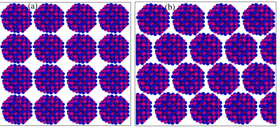
We consider 2D arrays of identical, nearly-spherical, perfectly passivated CQDs
(b)
(a)
Figure 1: Two-dimensional lattices considered in this work: (a) square lattice and (b) hexagonal lattice. The passivants are not shown.
dots face each other across the h100i facet, whereas in the latter across the h110i facet),
and we include only nearest neighbor interactions. We therefore neglect the effects of
trap/surface states, of thermal vibrations of the dots around their position (positional
disorder) and of potential mutual re-orientation of the dots. The electronic structure of
such CQD films is modelled using the tight-binding approach, traditionally employed
in the modelling of semiconductor bulk solids,29,30 with the difference that the atomic
orbitals and energies used in the latter are replaced here by the wave functions (and
eigenenergies) of the isolated CQD states, obtained within the framework of the
atom-istic semiempirical pseudopotential method.31
We focus on the lowermost miniband in the conduction band, i.e., that formed by the
1S state, as it is the one most likely to be involved in (dark) transport in these systems.
Nevertheless, we include up to 15 states in its calculation (i.e., we diagonalize a 15×15
matrix, including states laying few hundreds of meV above the 1S state), to account for
possible coupling effects to higher energy bands. All our states are doubly degenerate,
when pseudo-spin is included.
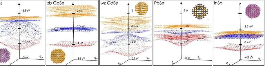
con-qy
−3 eV
PbSe InSb
wz CdSe zb CdSe
[image:7.595.84.541.72.189.2]InAs
Figure 2: Calculated 3D band structure for CQD films made of different materials (InAs - R=1.22 nm and an As-rich surface -, zinc blende CdSe - R=1.22 nm and a Cd-rich surface-, wurtzite CdSe -R=1.26 nm-, PbSe -R=1.26 nm - and InSb -R=1.31 nm -, all for a dot-to-dot separationd=1 bl. States with the same symmetry have the same color: red for the s-like ground state, blue for the p-like states, and orange for the d-like states. The inset in each panel displays the atomistic structure of the dots considered: brown spheres represent In atoms, violet As, pink Sb, yellow Cd, orange Se, and dark grey Pb.
sidered is shown in Figure 2, for dots with R≈1.2 nm and a dot-to-dot separationd of one bond length (1 bl =a0√3/4=0.26 nm for InAs and zinc-blende CdSe, where a0 is the bulk lattice constant). This is the shortest distance considered in this work.
Our results show that at this separation there is considerable inter-dot coupling in
many materials, leading to the formation of several sets of wide minibands. This can be
fully appreciated by considering Figure 2, which offers a 3D picture of this effect, where
minibands corresponding to states with the same prevalent angular momentum have the
same color (red for the s-like ground state; blue for the 3 p-like states and orange for the
d-like states).
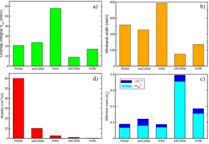
We find that the inter-dot coupling Vii=hψi(r)|V(r)|ψi(r−r′)i (Figure 3a) decreases
exponentially with distance for all materials, in agreement with the results of a previous
work on arrays of CdSe dots.32 This effect is shown in Fig. S1 (Supporting Information)
for the case of films of InAs CQDs withR=1.22 nm, where the effective masses calculated using Eq. (2) are shown, together with the corresponding miniband widths, as a function
of dot-to-dot separationd.
Given the extreme sensitivity of the film’s band structure to the inter-dot separation
A strong dependence of carrier mobility on the ligand length has also been established
in several recent experimental studies26,28,33 (although there are also indications34 that
the nature of the dot-ligand interaction is not always solely geometrical, but can also
involve electronic coupling,35 with non-trivial consequences on the film’s mobility. This
is especially true in the case of inorganic, i.e. halide, passivation).
The presence on the CQD surface of native bulky passivants limits their proximity and
represents a barrier to efficient charge transport between dots. The inter-particle
separa-tion can however be reduced, and the electronic coupling between CQDs enhanced, by
exchanging them for shorter ligands,36 or by removing them altogether via thermal
an-nealing.37,38The length of the capping agents routinely employed to stabilize the surface
of these nanostructures ranges from 2 nm for oleic acid,39 to 0.35 nm for oxalic acid.28
The use of inorganic ligands, such as atomic halide anions (Cl−, Br−and I−), can lead to a
further decrease of the inter-dot separation in a film down to 0.1 nm.20Furthermore, after
undergoing reactive self-assembly40–42 or laser annealing,43 the dots can bond
facet-to-facet preserving both crystalline atomic ordering across the interface and long range
or-der across the film and even form coherent percolative networks.44 All this experimental
evidence supports our choice ofd=1 bl (>0.2 nm) as an inter-dot separation realistically achievable in technologically relevant CQD films.
Starting from the calculated band structure, we extract miniband widths Wi (Fig-ure 3b) and effective massesm∗i (Figure 3c). The latter are calculated in two independent ways: (i) by fitting the calculated band structure around q=0 with a parabola
mi∗= h¯
2q2 i
2(Ei−E0) (1)
whereEiis the calculated energy at q=qi(forqiclose to 0), andE0is the energy atq=0,
and then taking the arithmetic average of the effective masses obtained along two
0 10 20 30 40 50 60
Overlap integral V
ss
(meV)
PbSe wzCdSe InAs zbCdSe InSb 0
100 200 300 400
Miniband width (meV)
PbSe wzCdSe InAs zbCdSe InSb
0 0.2 0.4 0.6 0.8
Effective mass (m
0
)
<m||*> mTB*
PbSe wzCdSe InAs zbCdSe InSb
0 10 20 30 40 50 60 Mobility (cm 2 /Vs)
PbSe wzCdSe InAs zbCdSe InSb
a) b)
[image:9.595.97.519.215.507.2]c) d)
Figure 3: Calculated overlap integralsVss=hψs(r)|V(r)|ψs(r−r′)i(a), miniband widths
(b), effective masses at Γ- using both Eq. (1) and Eq. (2) - (c), and mobilities (d), relative
tight-binding expression (Figure 3c, cyan bars)
m∗i(q=0) = βih¯
2
Wia2
(2)
whereβiis a constant that depends on the specific lattice and state i, anda=2R+dis the center-to-center distance between nearest-neighbor CQDs (more details can be found in
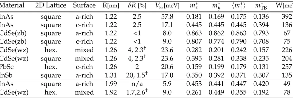
[image:10.595.80.590.427.598.2]the Supporting Information). The results are presented in Figure 3 and Table 1, for d=1 bl.
Table 1: Calculated overlap integrals (Vss), miniband widths (W) and effective masses at
Γ(m∗
x andm∗y are obtained alongxand yby fitting the miniband curvature aroundq=0
with a parabola, according to Eq. (1), hm∗ki = (m∗x+m∗y)/2, is their arithmetic average, whereasm∗TBare calculated using Eq. (2)) atd=1 bl, for different materials, radii (R), and surface terminations (CdSe dots in the wurtzite phase exhibit ’mixed’ surfaces, with no clear prevalence of a specific atomic species at the interface with the neighboring dots).
δR represents the threshold size distribution that satisfies Vii = ∆E= |Ei(R)−Ei(R± RδR/100)|, at which Anderson localization effects start to occur (†for wz CdSe and InSb two values forδRare reported, as theEivs Rcurve is not a straight line in this case, but has a different slope in the direction of larger sizes [first value in column 4] from that towards smaller sizes [second value in column 4]).
Material 2D Lattice Surface R[nm] δR[%] Vss[meV] m∗x m∗y hm∗ki m∗TB W[meV
InAs square a-rich 1.22 2.5 57.8 0.181 0.169 0.175 0.136 392 InAs square c-rich 1.22 2.5 17.1 0.445 0.445 0.445 0.394 136 CdSe(zb) square a-rich 1.22 <1 8.0 0.863 0.862 0.863 0.793 67 CdSe(zb) square c-rich 1.22 <1 9.0 0.807 0.774 0.790 0.708 75 CdSe(wz) hex. mixed 1.26 4, 2.3† 23.6 0.282 0.201 0.242 0.157 226 CdSe(wz) square mixed 1.26 4, 2.3† 23.6 0.395 0.281 0.338 0.235 204
PbSe hex. c-rich 1.26 2 20.6 0.159 0.199 0.179 0.131 257
InSb square a-rich 1.31 20, 1.5† 17.0 0.350 0.392 0.371 0.307 135 InAs square a-rich 1.99 n/a 5.9 0.453 0.441 0.447 0.420 49 CdSe(wz) hex. mixed 1.92 1.7,2.6† 9.0 0.261 0.449 0.355 0.192 78
Since our 2D arrays are made of identical CQDs, another important point is to de-termine to what extent this condition is responsible for the formation of wide minibands
with their associated small effective masses, in close packed films, or, in other words, how
chemi-cally synthesized in the lab. The main issue here is Anderson’s localization,45 the most
likely origins of which have been identified46 to be (i) size and (ii) positional disorder.
Localization occurs when the energy broadening caused by disorder is larger than the
coupling between neighboring sites Vii (i = s,p,d, . . . is the angular momentum of the dots’ wave functions). Our present model is unfortunately unable to estimate the energy
spread due to fluctuations in the dot position. We will therefore address the effects of
size distribution on the realization of the conditions for bulk-like transport. Indeed it has
been recently pointed out47 that this is probably the main source of energy fluctuations
in arrays of CQDs. The energy spread due to size distribution ∆E must satisfy∆Ei<Vii for the array to be free from localization effects due to size fluctuations. Our calculated
overlap integrals for the 1S state, Vss, are presented in Figure 3a and Table 1, where the
corresponding values for the size distribution are also shown. In films of InAs CQDs,
for example, Vss =58 meV for d=1 bl andVss=18.5 meV ford=1.6 bl (not shown in
Table 1). This corresponds to size distributions<2.5%, and<1%, respectively. While the
former could be achievable with modern growth methods, the latter is not within their
reach yet. Some localization effects caused by size variations could therefore be expected
in films of small (R∼1.2 nm) InAs CQDs separated by more than 1 bl for transport in the lowest miniband.
The widest ground state miniband, with one of the smallest associated effective masses,
is found in InAs. Interestingly a film of zinc-blende CdSe CQDs with the exact same
total number of atoms as the InAs dots and, due to the similarity of the lattice
con-stants between the two materials - 0.6058 nm vs 0.6081 nm - also essentially the same
size [R(InAs)=1.220 nm vs R(CdSe)=1.225 nm, as calculated based on the total number of
atoms and assuming a spherical shape48], exhibits 1S miniband widths (effective masses)
a factor of over 5 narrower (larger). This effect can be attributed to the different values
of the electron effective masses in the two bulk materials. Indeed it has been observed32
inverse of the bulk effective mass.
The same is not true, however, for the third (1d) miniband, which exhibits a width of
about 300 meV at 1 bl, as a result of the coupling of up to 6 states. This coupling persists
for separations of 1.3 bl (when the band width decreases to about 210 meV), but is broken
at 1.6 bl, when the lowermost doublet decouples from the higher energy multiplet of four
states. The latter forms a miniband whose width (∼135 meV) is similar to that of the
1S and 1P bands calculated for InAs dots of the same size at the same distance. Efficient
transport could therefore be achievable in zinc-blende CdSe CQDs even at this separation,
provided the doping level is high enough so that this high band can be populated.
According to theeffective mass rule32 mentioned above, wider minibands and smaller associated effective masses are expected for 2D arrays of CQDs made of materials with
small bulk effective masses. We tested this hypothesis in the case of InSb, whose bulk
ef-fective mass is a factor of∼2 smaller than that in InAs, and therefore promises miniband
widths of the order of ∼800 meV. Furthermore this material exhibits, in the bulk, the
highest electron mobility among all semiconductors, and is therefore a good candidate
for testing transport properties at the nanoscale. The results, displayed in Figure 3 and
Table 1, contradict these expectations, exhibiting widths about 1/3 of those calculated
in the case of InAs dots with the same number of anions and cations (however slightly
different in size, owing to the different lattice constant between InSb and InAs), and
ef-fective masses over 2 times larger. The origins of this surprising behavior are unclear. We
suggest that they may be related to the peculiar electronic structure ofsmallInSb CQDs, where a k-space decomposition analysis of the conduction band minimum (CBM) wave
function recently evidenced49a large contribution from the L-point in the Brillouin zone,
in contrast to the case for InAs dots of the same size. The presence of such high-frequency
components could adversely affect the overlap integrals and therefore the miniband
ef-fective masses.
ex-tensive exploitation in next generation CQD-based solar cell devices, is PbSe. As its
pe-culiar electronic structure, with a direct band gap situated at the L point in the Brillouin
zone,50 yields 8-fold degenerate band edges in the bulk, arrays of CQDs of this material
may have the potential to form very wide minibands. Indeed, it is easy to show that,
according to the tight-binding model, a lattice made of dots with an N-fold degenerate
1S-type spherically symmetric identical ground state results in an (N-1)-fold
degener-ate, perfectly flat band plus a single band at lower energies, whose width is N times the
width exhibited by the lowest miniband in an array of dots with asingle, non-degenerate 1S ground state, arranged in the same lattice. Considering that in a PbSe CQD the 8-fold
degeneracy of the bulk band edge states is lifted,50leaving a two-fold degenerate ground
state (4-fold including spin) and two singly-degenerate higher levels (doubly-degenerate
with spin), and that the wave functions of these states are not exactly the same, our
find-ings of 3 nearly flat bands with slightly different energies, plus a 260 meV wide ground
state (Figure 2) are consistent with the tight-binding predictions.
Experimentally, films of PbSe CQDs have been observed to assemble in square,42
hon-eycomb42 and and hexagonal51 lattices. In Figure 2 we present the band structure
calcu-lated assuming an hexagonal configuration. Our results show that films of CQDs made
of PbSe exhibit the smallest effective mass and one of the largest miniband widths of all
materials considered (see Figure 3 and Table 1): these systems are therefore potentially
ideally suited for a wide variety of optoelectronic applications requiring good transport
properties.
An interesting question is whether the transport properties of a material are affected
by its crystal structure and, if so, to what extent. The band structure parameters calculated
for films made of zinc blende and wurtzite CdSe CQDs (the latter are assumed to be
arranged either in an hexagonal lattice, with their c axis aligned perpendicular to the film
plane, or in a square lattice), of similar sizes (1.22 nm and 1.26 nm, respectively) can be
zinc-blende in terms of transport, exhibiting a 1S miniband width a factor of∼3 wider
than the zinc-blende phase (and effective masses about the same factor smaller) for the
closest inter-dot separation. It is clear, however, that the 1S miniband width of wurtzite
CdSe CQDs remains smaller than that obtained in the case of similarly sized InAs dots. As
the bulk effective masses of CdSe are nearly the same in both the cubic and the hexagonal
modification, this large difference in transport properties represents another violation of
the simplisticeffective mass rule.
A further question arises regarding the effect of the different lattice arrangements of
the dots (square vs hexagonal) on the array’s band structure. Our results for films of
wurtzite CdSe dots predict better transport properties for hexagonal (hex) lattices,
com-pared to square (sq) ones, (provided that the dots are the same and their separation is the
same in both arrays), and yield a miniband effective mass ratiom∗sq/m∗hex of 1.4, in good agreement with the standard tight-binding theory, which, in the case of perfectly
decou-pled bands, predicts (see Eq. S1 in the Supporting Information) the ratio of the miniband
effective masses in 2D square and hexagonal lattices to be 1.5, i.e., inversely proportional
to the ratio of the number of nearest neighbors in the two arrangements (4/6).
The transport properties of CQD films are also found to be strongly size dependent,
and more markedly so for III-V materials: two examples - InAs and wurtzite CdSe - are
provided in Table 1 (further details on the size-dependence of the band structure
param-eters can be found in the Supporting Information). In the former material, the miniband
widths of 2D arrays of CQDs with R =1.99 nm are a factor of about 8 narrower than those obtained for dots with R=1.22 nm, (and the effective masses about 3 times heav-ier), whereas in the case of CdSe, the difference in miniband width between films of dots
with R =1.26 nm and R =1.92 nm drops to a factor of about 3 (1.5 for the effective masses). This size-dependence is due to a reduction in the overlap integral with
increas-ing dot size, an effect common to all materials, result of the space normalization of the
electron anywhere in the dot - given by the integral over the dot volume of the wave
function squared - is 1, the probability of finding it at any specific location within the dot
- given by the amplitude of the wave function at that location - decreases with increasing
dot volume).
Given that, as we have seen, the inter-dot separation is a crucial parameter
determin-ing the width of the minibands and the magnitude of the associated effective masses,
an interesting question is whether the detailsof the surfaces of the nanostructures facing each other have any influence on the strength of their coupling, hence on the electronic
structure of the 2D array. Figure S2 (Supporting Information) compares the miniband
widths and effective masses calculated for films of InAs dots with the same nominal size
(R=2 nm) but with slightly different surface morphologies: in case (i) the surfaces
fac-ing each dot terminate with a flat facet of In atoms; in case (ii) these surfaces have two
added As atoms, and have therefore a ”bumpy" profile; finally, in case (iii) the two As
atoms on the surface of one dot interlock with the atoms on the surface of the other, like
two LEGO bricks (Although cases (ii) and (iii) may seem artificial and perhaps
unrealis-tic, they allow us to investigate the effects on the film’s electronic structure and mobility
of some degree of surface roughness that may be found in experimental samples). We
find that the miniband width in cases (i) and (ii) scales with the number of outermost
surface atoms (i.e., those facing each other at the dot-to-dot interface), whereas in case
(iii) it is enhanced compared with case (i), due to the enhanced coupling caused by the
interdigitation (this effect is highlighted by the non-exponential behaviour of both width
and effective masses for negative distances - see first point in the red curves of Figure S2
(Supporting Information). These results highlight the importance of a clean flat surface in
order to obtain strong inter-dot couplings and good transport properties. However, they
also suggest that even stronger couplings are achievable in interlocked dots, indicating
possible new strategies to enhance transport in these systems.
species terminating the surface may influence the strength of the interdot coupling in a 2D array. We investigated this effect by comparing the electronic structure calculated for
films made of InAs and zinc blende CdSe dots with R=1.22 nm with anion- and
cation-terminated surfaces. In both InAs and zinc blende CdSe dots the total number of atoms
is the same (275) and the number of anions and cations in each is almost identical (140
vs 135). Our results (Table 1 and Fig. S1 - Supporting Information) exhibit, however,
a strikingly different behavior in the two materials: anion-terminated structures yield
stronger coupling, hence better transport properties, in InAs, whereas the opposite is true
for zinc blende CdSe. This effect is, however, much stronger in arrays of InAs dots, where
the enhancement is three-fold, than in zinc blende CdSe films, where the variation in the
coupling is just 10%.
Once more the surfacedetailsare found to have a profound influence on the dot-to-dot interactions in multidimensional arrays.
All the quantities in Figure 3a, b, and c are consistent, so that the material with the
largest interdot coupling (InAs, Figure 3a) also exhibit the widest miniband (Figure 3b)
and the smallest effective mass (Figure 3c), and, vice versa, films of zinc blende CdSe, where the coupling is weakest, have the narrowest miniband and the largest effective
masses. The same is however not true for the mobility (Figure 3d): surprisingly there is
little relationship between the electron effective mass and its mobility within a miniband.
Assuming that the electrons are scattered by fluctuations in the dot size alone,47 we
derive the following expression for an order-of-magnitude estimate of the mobility in the
lowest miniband of a CQD film52
µOM(ρdefects,δR) =
eh¯3
m∗2ρ
defectsMA
(3)
is the effective mass of the miniband obtained using Eq. (1) (further details are available
in the Supporting Information).
According to these estimates, mobilities∼1 cm2V−1s−1are achievable in CQD arrays
of almost all materials considered. This is an important threshold for achieving rapid
exciton dissociation for PV applications. Indeed it has been shown33 that for mobilities
in excess of 1 cm2V−1s−1, all photogenerated electron-hole pairs separate rapidly enough
to escape Auger recombination and the carrier multiplication efficiency in CQD films
[image:17.595.94.513.510.679.2]approaches the value observed in dot dispersions.
Table 2: Order-of-magnitude [a] and maximum [b] in-plane dark mobilities (in cm2 V−1s−1) calculated at room temperature for "touching dots" using Eq. (3) [a] and Eq. (4) [b] (as this expression was derived for cubic lattices, the mobility was rescaled by a fac-tor of 1.52in the case of hexagonal lattices to account for the difference in the miniband effective masses in the two configurations - see text), for different materials, dot radii and surface terminations (CdSe dots in the wurtzite phase exhibit ’mixed’ surfaces, with no clear prevalence of a specific atomic species at the interface with the neighboring dots). The values for the electron confining potentials (U0) and assumed size distribution (χ) are also reported (the calculated overlap integralsVssare listed in Table 1), Owing to the
atomistic nature of our approach, it was difficult to achieve the same relative size differ-ence for all dots, and it was impossible to obtain values lower than 8%, while keeping a nearly spherical shape, when most of the CQDs radii were close to 1.2 nm. This is why we used similar but different values forχfor different materials and dot sizes. For ease of comparison with the results of ref.,47 the mobilities calculated with Eq. (4) using a 5% size distribution are also reported (in brackets) next to those obtained for the different values ofχreported in the third column. A 1% density of defects was assumed in Eq. (3).
Material Lattice Surface R[nm] U0[eV] χ[%] µdOM[a] µmaxd [b] (χ=5%)
PbSe hex. c-rich 1.26 4.56 9.2 65 1.8 (6.1) CdSe(wz) hex. mixed 1.26 3.59 10.4 11 3.1 (13.7) CdSe(wz) square mixed 1.26 3.59 10.4 4.7 1.4 (6.1) InAs square a-rich 1.22 5.16 8.4 2.6 9.2 (26.0) InAs square c-rich 1.22 5.16 8.4 0.8 0.4 (1.2) CdSe(zb) square c-rich 1.22 3.48 8.5 1.0 0.2 (0.6) CdSe(zb) square a-rich 1.22 3.48 8.5 0.7 0.1 (0.4) InSb square a-rich 1.31 4.75 8.6 0.2 0.6 (1.6) CdSe(wz) hex. mixed 1.92 3.59 7.6 5 1.3 (2.9) InAs square a-rich 1.99 5.16 8.0 0.4 0.1 (0.2)
su-percrystal, valid under the assumption that fluctuations in the size of the CQDs represent
the main source of electron scattering (small radius limitqR<<1), was recently derived within the framework of the k·p approach by Shabaev, Efros and Efros.47 In the case of
touching dots this reduced to47
µmaxd = 28
3π3/2 eR2
¯
h t5/2
χ2U2
0
1
√
kBT
(4)
where t is the overlap integral, χ the size dispersion, U0 the confining potential for the electrons, T the temperature and kB the Boltzmann constant. As the plane overlap in-tegrals are independent of the dimensionality of the array, we can substitute in Eq. (4)
our calculated values forVii=tandU0 (also reported in Table 2) to obtain estimates for
the maximum in-plane dark mobilities achievable in arrays of CQDs of different
materi-als, according to Eq. (4). A comparison between the predictions of the latter and those
obtained using our approach (Eq. (3)) is presented in Table 2 (as (4) was derived for
cubic lattices, the mobility in the last column of the table was rescaled by a factor of
(m∗sq/m∗hex)2= (3/2)2in the case of hexagonal lattices - PbSe and wzCdSe - to account for
the difference in the miniband effective masses in the two configurations, see below).
We find (Figure 3d, and Table 2) that the mobility exhibits strong variations from
ma-terial to mama-terial (when considering dots with the same size), from crystal structure to
crystal structure (when considering dots of the same material), from lattice type to lattice
type (when considering dots of same size, material and crystal structure), and from size
to size (when considering dots of the same material and crystal structure): arrays of PbSe
CQDs exhibit the highest mobilities, consistent with the values recently observed in these
systems,17 whereas, surprisingly, the lowest values are obtained for InSb, which boasts,
instead, the highest mobility of all semiconductors in the bulk (if compared with films of
InAs dots, with which they share very similar material properties, the main origin of the
the mobility in CdSe films is about 5 times larger for dots in the wurtzite phase than for
those in the zinc blende crystal structure, despite the significant difference in size
distri-bution between the two films whereχ(wz)>χ(zb);552D hexagonal lattices exhibit larger
mobilities than square ones, mainly owing to the difference in their respective miniband
effective masses (withm∗sq ≈1.5m∗hex), leading to an increase by a factor of∼1.52=2.25 (due to them∗−2dependence in (3)) in the mobility of hexagonal lattices (the ratio between the mobilities we calculate in hexagonal and square lattices of wurtzite CdSe CQDs is
in-deed 2.3); finally, arrays of InAs dots of different sizes (R=1.2 nm vsR=2.0 nm) display larger differences in mobility (about a factor of 6) compared to films of similarly sized
wurtzite CdSe dots (where larger structures exhibit mobilities only a factor of 2 smaller).
In particular we found that arrays of wurtzite CdSe CQDs with D=3.8 nm can exhibit mobilities of the order of ∼12 cm2 V−1s−1, if the dots are placed at a distance of 1 bl
(0.26 nm) and have a size distribution of 5% (data not shown in Table 2, where we report
our results forχ=7.6 for a fairer comparison with the other sizes and materials). These
estimates are consistent with the dark mobilities (27 cm2V−1s−1)13observed
experimen-tally in these systems, and in sharp contrast to the predictions of Eq. (4), which yields
(when the resulting mobility is multiplied by a factor of 2.25 to account for the different
- i.e. hexagonal - lattice type), for the same system, amaximum achievable mobilityover a factor of 4 smaller than ours and nearly one order of magnitude smaller than experiment.
Similarly, in the case of films of “touching” PbSe CQDs withD=2.52 nm (and a size dis-tribution of 9%) we predict mobilities around 65 cm2 V−1s−1 (vs 1.8 cm2 V−1s−1, using
Eq. (4) adjusted for an hexagonal lattice), which are in good agreement with recently
re-ported electron mobilities17 (10 cm2V−1s−1), if considering that the latter were obtained
in films made of larger dots (D=6 nm) and with a narrower size distribution. Interest-ingly the experimental samples where such record-high mobilities were observed had a
Pb-rich surface, like the dots considered here (see inset of panel 4 in Figure 2), where the
PbSe films when the dots are ’fused’ together and connected by necks with thicknesses
close to the dots’ diameters, forming percolative networks.44 However, as such systems
exhibit uninterrupted segments of attached CQDs, whose length may even approach the
distance between electrodes, their transport properties are very different from those of
the films considered in the present work, where the dots do not touch.
In comparing our results with those of Shabaevet al.,47 it is worth pointing out that, unlike in ref.,47 here we do not treatU0 as a fitting parameter. As in the calculation of
the isolated dot wave functions we take the vacuum level as a reference zero energy, for
a meaningful comparison between the results of Eq. (3) and Eq. (4), the depthU0 of the
electron well (see Table 2) is determined consistently within the atomistic semiempirical
pseudopotential framework, i.e., as the absolute value of the calculated position of the
conduction band, in the limit of infinitely large dots (which is in good agreement with the
asymptotic behavior observed in recent accurate photoelectron spectroscopic
measure-ments53). Any reduction in the electron confinement would lead to a substantial increase
in the mobilities, owing to the combined effect of an increase in the overlap integral t
(raised to the power of 5/2 in the numerator of Eq. (4)) and a decrease ofU0 (raised to
the power of 2 in the denominator of Eq. (4)). As an example, a reduction of 0.5 [1.0] eV
inU0 alone (i.e., without considering the corresponding increase of the overlap integral
t=Vss) would lead to a 25% [54%] increase in the mobility calculated for an array of InAs
dots with R=1.2 nm. In this respect, we note that in order to reproduce the experimental
dark mobilities measured in ref.,13Shabaev and Efros must assume unrealistic values for
U0(i.e.,<1 eV), which are more suitable to epitaxial dots, than colloidal nanostructures.
This is because the continuum-like approach of ref.47 largely underestimates the overlap
integrals t. Indeed, in order to obtain the same values for t we calculated for arrays of touching wurtzite CdSe CQDs (see Table 1), Shabaev and Efros need to assume a
con-fining potential about 3 eV smaller (0.6 eV) than the one used in our atomistic approach
Furthermore, while the mobility in Eq. (3), together with an inverse dependence on the
size difference between nominal-size dots and scatterers (expressed through the matrix
element M), also exhibits a crucial inverse dependence on the density of the scattering centers, as one would expect, Equation (4) only accounts for the former through the size
dispersion χ, but lacks any explicit dependence on the latter. On the other hand, unlike
in Eq. (4), there is no temperature dependence in Eq. (3), consistently with the expected
temperature independence of the scattering mechanism considered in this work, where
the defect density does not depend on temperature.54
In our investigation we find that the value of the mobility is influenced by many
dif-ferent factors, among which the miniband’s effective mass represents an important - but
not the only important - contribution. A paramount role is played by the material, and by
that we mean the nanoscopic details of the atomic potentials, as∆V (the perturbation in
the potential due to a difference in dot size, which appears in the integrals in the mobility
calculations Eq. (3), in the case of size-fluctuation-governed scattering), can vary by
or-ders of magnitude between two different materials, even when the CQDs have the same
configuration at the atomic level, as in the case of InAs and zinc-blende CdSe dots (which
have the same number of atoms arranged in nearly identical positions). The magnitude
and symmetry of the electron wave functions in the region where∆Vis non-zero are also
crucial to the evaluation of the mobility integrals. It is therefore difficult to infer relative
values for the mobility of different materials simply based on their respective miniband
effective masses (which depend on the value of the overlap integralhψi(r)|V(r)|ψi(r−r′)i
- a fundamentally different quantity from the perturbation integralhφi(r)|∆V(r)|φ
i(r)i),
as the results presented in Table 2, Table 1 and Figure 3 confirm. Indeed, the above factors
sometime combine to yield unexpected results, such as in the case of PbSe or zinc-blende
CdSe (where the former, despite having an effective mass similar to InAs, exhibits a
mo-bility over 22 times larger, and the latter, with an effective mass over 5 times heavier than
con-tributions. It is important to stress that, owing to its distinctive features, this effect can
only be captured within the framework of an atomistic approach and is therefore beyond
the reach of continuum-like methods, such as the popular k·p approach.
We should also mention here that, as our single-dot calculations are performed in
vacuum (which condition places the strongest constraints on the extension of the wave
functions outside the dot, hence on the magnitude of inter-dot coupling), our estimates
for miniband widths [effective masses] and associated mobilities represent lower [upper]
limits for these quantities.
In conclusion, we investigated the effects of size, crystal structure, material
composi-tion, stoichiometry, surface morphology and dot-to-dot separation on the band structure
parameters and electron mobilities in CQD films. Our results evidence a surprising
in-dependence of the film’s transport properties from those of the bulk material from which
the dots are made, and indicate a strong influence of the dot’s structural characteristics
(crystal structure, stoichiometry and morphology) on the resulting film mobilities. InAs
dots exhibit the widest minibands, with associated smallest effective masses, however
the largest mobilities of all materials considered - of the order of tens of cm2V−1s−1- are
found in PbSe (these values are consistent with the highest mobilities recently reported
for thin films of PbSe CQDs17), whereas 2D arrays of InSb dots are predicted to exhibit
the lowest mobility of all materials considered, despite the record-high mobility observed
in that material in the bulk. By comparing 2D arrays made of the same material but with
different crystal structures, we show that wurtzite outperforms zinc-blende in terms of
transport properties, exhibiting mobilities about one order of magnitude larger. Our
cal-culated mobilities for 2D arrays of wurtzite CdSe dots are also consistent with recent
ex-perimental measurements.13 Our results further show that smaller dots exhibit stronger
coupling, hence wider minibands and higher mobilities. A crucial aspect determining
the coupling strength between adjacent dots is found to be their surface morphology:
other across the inter-dot gap, provide the best interface for strong dot-to-dot
interac-tion, whereas in the presence of rough surfaces, where a few adatoms protrude from the
surface, the extent of wave function overlap is limited to these few atoms, reducing the
overall electronic coupling (which is proportional to the number of atoms on the surfaces
facing each other), for the same nominal inter-dot separation and dot size. Interestingly
we find that stoichiometry also plays an important role in determining the transport
prop-erties of dot arrays. This effect is found to be stronger in III-V materials than in II-VI. Our
results also highlight a non-trivial relationship between the mobility of an electron and its
effective mass within a miniband, that can only be captured by considering the atomistic
details of the material and is therefore outside the reach of continuum-like methods, such
as the popular effective mass k·p approach. This work represents a crucial step in the
effective design and optimisation process of CQD films for specific device applications.
Acknowledgement
M.C. gratefully acknowledges financial support from the Royal Society under the URF
scheme, and from GENIL - Strengthening through Short-Visits Ref. GENIL-SSV 2014.
F.M.G.C. and S.R.B. were supported by Project TEC2013-47283-R, funded by the Spanish
Secretaria de Estado de Investigación, Desarrollo e Innovación, Ministerio de Economía y
Competitividad; F.M.G.C. was also funded by Project mP_TIC_5 from Campus de
Ex-celencia Internacional BioTic Granada; and a mobility grant from the "José Castillejo"
program for young researchers funded by Spanish Ministerio de Educación, Cultura y
Deporte.
Supporting Information Available
Atomistic modelling of single CQDs, Tight-binding band structure parameters,
the band structure, Effect of different surface morphologies, An order-of-magnitude
ex-pression for the mobility This material is available free of charge via the Internet at
http://pubs.acs.org.
References
(1) Califano, M.; Gomez-Campos, F. M.Nano Lett.2013,13, 2047-2052.
(2) Yu, D.; Wang, C.; Guyot-Sionnest, P.Science2003300, 1277-1280.
(3) Vanmaekelbergh, D.; Liljeroth, P.Chem. Soc. Rev.2005,34, 299-312.
(4) Kovalenko, M. V.; Scheele, M.; Talapin, D.V.Science2009324, 1417-1420.
(5) Wehrenberg, B. L.; Yu, D.; Ma, J. S.; Guyot-Sionnest, P. J. Phys. Chem. B 2005, 109, 20192-20199.
(6) Chandler, R. E.; Houtepen, A. J.; Nelson, J.; Vanmaekelbergh, D. Phys. Rev. B 2007,
75, 085325/1-085325/10.
(7) Yu, D.; Wang, C.; Wehrenberg, B. L.; Guyot-Sionnest, P. Phys. Rev. Lett. 2004, 92, 216802.
(8) Liu, H.; Pourret, A.; Guyot-Sionnest, P.ACS Nano2010,4, 5211-5216.
(9) Chu, I.-H.; Radulaski, M.; Vukmirovic, N.; Cheng, H.-P.; Wang, L.-W. J. Phys. Chem. C2011,115.
(10) Mentzel, T. S.; Porter, V. J.; Geyer, S.; MacLean, K.; Bawendi, M. G.; Kastner, M. A.
Phys. Rev. B2008,77, 075316.
(12) Mentzel, T. S.; Wanger, D. D.; Ray, N.; Walker, B. J.; Strasfeld, D.; Bawendi, M. G.;
Kastner, M. A.Nano Lett.2012,12, 4404-4408.
(13) Choi, J.-H.; Fafarman, A. T.; Oh, S. J.; Ko, D. K.; Kim, D. K.; Diroll, B. T.; Muramoto,
S.; Gillen, J. G.; Murray, C. B.; Kagan, C. R.Nano Lett.2012,12, 2631-2638.
(14) Lee, J.-S.; Kovalenko, M.; Huang, J.; Chung, D. S.; Talapin, D. Band-like transport,
high electron mobility and high photoconductivity in all-inorganic nanocrystal
ar-rays.Nat. Nanotechnol.2011,6, 348-352.
(15) Talgorn, E.; Gao, Y.; Aerts, M.; Kunneman, L. T.; Schins, J. M.; Savenije, T. J.; van Huis,
M. A.; van der Zant, H. S. J.; Houtepen, A. J.; Siebbeles, L. D. A.Nat. Nanotechnol.
2011,6, 733-739.
(16) Yang, Y.; Liu, Z.; Lian, T.Nano Lett.2013,13, 3678-3683.
(17) Oh, S. J.; Berry, N. E.; Choi, J.-H.; Gaulding, E. A.; Paik, T.; Hong, S.-H.; Murray, C.
B.; Kagan, C. R.ACS Nano2013,7, 2413-2421.
(18) Oh, S.; Wang, Z.; Berry, N.; Choi, J., Zhao, T.; Gaulding, E. A.; Paik, T.; Lai, Y.; Murray,
C. B.; Kagan, C. R.Nano Lett.2014,14, 6210-6216.
(19) Ip, A. H.; Thon, S. M.; Hoogland, S.; Voznyy, O.; Zhitomirsky, D.; Debnath, R.;
Lev-ina, L.; Rollny, L. R.; Carey, G. H.; Fischer, A.; Kemp, W. K.; Kramer, I. J.; Ning, Z.;
Labelle, A. J.; Chou, K. W.; Amassian, A.; Sargent, E. H. Nat. Nanotechnol. 2012, 7, 577-582.
(20) Tang, J.; Kemp, K. W.; Hoogland, S.; Jeong, K. S.; Liu, H.; Levina, L.; Furukawa, M.;
Wang, X.; Debnath, R.; Cha, D.; Chou, K. W.; Fischer, A.; Amassian, A.; Asbury, J. B.;
and Sargent, E. H.Nat. Mater.2011,10, 765-771.
(21) Ning, Z.; Voznyy, O.; Pan, J.; Hoogland, S.; Adinolfi, V.; Xu, J.; Li, M.; Kirmani, A.
Sutherland, B.; Hill, I.; Amassian, A.; Liu, H.; Tang, J.; Bakr, O. M.; Sargent, E. H.Nat. Mater.2014,13, 822-828.
(22) Zhang, J.; Gao, J.; Miller, E. M.; Luther, J. M.; Beard, M. C.ACS Nano 2014,8, 614-622.
(23) Chuang, C. M.; Brown, P. R.; Bulovic´, V.; Bawendi, M. G.Nat. Mater.2014,13, 796-801.
(24) Woo, J. Y.; Ko, J.; Song, J. H.; Kim, K.; Choi, H.; Kim, Y.; Lee, D. C.; Jeong, S.; Song,
H.J. Am. Chem. Soc.2014,136, 8883-8886.
(25) Straus, D. B.; Goodwin, E. D.; Gaulding, E. A.; Muramoto, S.; Murray, C. B.; Kagan,
C. R.J. Phys. Chem. Lett.2015,6, 4605-4609.
(26) Liu, Y., Gibbs, M.; Puthussery, J.; Gaik, S.; Ihly, R.; Hillhouse, H. W.; Law, M.Nano Lett.2010,10, 1960-1969.
(27) Gao, Y.; Talgorn, E.; Aerts, M.; Trinh, M. T.; Schins, J. M.; Houtepen, A. J.; Siebbeles,
L. D. A.Nano Lett.2011,11, 5471-5476.
(28) Gao, Y.; Aerts, M.; Sandeep, C. S. S.; Talgorn, E.; Savenije, T. J.; Kinge, S.; Siebbeles,
L. D. A.; Houtepen, A. J.ACS Nano2012,6, 9606-9614.
(29) Slater, C.; Koster, G. F.Phys. Rev.1954,94, 1498-1524.
(30) Ashcroft, N. W.; Mermin, N. Solid State Physics, Holt Rinehart and Winston, New York, London, 1976.
(31) Wang, L.-W.; Zunger, A.Phys. Rev. B1996,53, 9579.
(32) Delerue, CPhys. Chem. Chem. Phys.2014,16, 25734-25740.
(33) Sandeep, C. S. S.; ten Cate, S.; Schins, J. M.; Savenije, T. J.; Liu, Y.; Law, M.;
(34) Sandeep, C. S. S.; Azpiroz, J. M.; Evers, W. H.; Boehme, S. C.; Moreels, I.; Kinge, S.;
Siebbeles, L. D. A.; Infante, I.; Houtepen, A. J.ACS Nano2014,811499-11511.
(35) Giansante, C.; Infante, I.; Fabiano, E.; Grisorio, R.; Suranna, G. P.; Gigli, G. J. Am. Chem. Soc.2015,137, 1875-1886.
(36) Talapin, D. V.; Murray, C. B.Science2005,310, 86-89.
(37) Drndic, M.; Jarosz, M. V.; Morgan, N. Y.; Kastner, M. A.; Bawendi, M. G.J. Appl. Phys.
2002,92, 7498-7503.
(38) Talgorn, E.; Abellon, R. D.; Kooyman, P. J.; Piris, J.; Savenije, T. J.; Goossens, A.;
Houtepen, A. J.; Siebbeles, L. D. A.ACS Nano2010,4, 1723-1731.
(39) Quan, Z.; Loc, W. S.; Lin, C.; Luo, Z.; Yang, K.; Wang, Y.; Wang, H.; Wang, Z.; Fang,
J.Nano Lett.2012,12, 4409-4413.
(40) Cho, K.-S.; Talapin, D. V.; W. Gaschler, W.; Murray, C. B.J. Am. Chem. Soc.2005, 127, 7140-7147.
(41) Schliehe, C.; Juarez, B. H.; Pelletier, M.; Jander, S.; Greshnykh, D.; Nagel, M.; Meyer,
A.; Foerster, S.; Kornowski, A.; Klinke, C.; Weller, H.Science2010,329, 550-553.
(42) Evers, W. H.; Goris, B.; Bals, S.; Casavola, M.; de Graaf, J.; van Roij, R.; Dijkstra, M.;
and Vanmaekelbergh, D.Nano Lett.2013,13, 2317-2323.
(43) Treml, B. E.; Robbins, A. B.; Whitham, K.; Smilgies, D.-M.; Thompson, M. O.; and
Hanrath, T.ACS Nano2015,9, 4096-4102.
(44) Evers, W. H.; Schins, J. M.; Aerts, M.; Kulkarni, A.; Capiod, P.; Berthe, M.; Grandidier,
B.; Delerue, C.; van der Zant, H. S. J.; van Overbeek, C.; Peters, J. L.; Vanmaekelbergh,
D.; Siebbeles, L. D. A.Nat. Commun.2015,6, 8195, DOI: 10.1038/ncomms9195.
(46) Guyot-Sionnest, P.J. Phys. Chem. Lett.2012,3, 1169-1175.
(47) Shabaev, A; Efros, Al. L; Efros, A. L.Nano Lett.2013,13, 5454-5461.
(48) Franceschetti, A.; Fu, H.; Wang, L.-W. & Zunger, A.Phys. Rev. B1999,60, 1819-1829.
(49) Sills, A.; Harrison, P.; Califano, M.J. Phys. Chem. Lett.2016,7, 31-35.
(50) An, J. M.; Franceschetti, A.; Dudiy, S.V.; Zunger, A.Nano Lett.2006,6, 2728-2735.
(51) Goodfellow, B. W.; Yu, Y.; Bosoy, C. A.; Smilgies, D.-M.; Korgel, B. A. J. Phys. Chem. Lett.2015,6, 2406-2412.
(52) Gómez-Campos, F. M.; Rodríguez-Bolívar, S.; Califano, M. (unpublished)
(53) Jasieniak, J; Califano, M.; Watkins, S. E.ACS Nano2011,5, 5888-5902.
(54) Yu, P.; Cardona, M. Fundamentals of Semiconductors: Physics and Materials Properties, 4th edition; Springer, Berlin, Heidelberg, 2010. ISBN 978-3-642-00709-5.
(55) A larger size distribution leads to a smaller electron mobility, given the position of
![Table 2: Order-of-magnitude [a] and maximum [b] in-plane dark mobilities (in cm2V−1s−1) calculated at room temperature for "touching dots" using Eq](https://thumb-us.123doks.com/thumbv2/123dok_us/7842948.176950/17.595.94.513.510.679/table-order-magnitude-maximum-mobilities-calculated-temperature-touching.webp)
