energies
Article
Design and Analysis of Nano-Structured Gratings for
Conversion Efficiency Improvement in GaAs
Solar Cells
Narottam Das1,2,* and Syed Islam2
1 School of Mechanical and Electrical Engineering, University of Southern Queensland,
Toowoomba, QLD 4350, Australia
2 Department of Electrical and Computer Engineering, Curtin University, Perth, WA 6845, Australia;
* Correspondence: [email protected]; Tel.: +61-746-311-195
Academic Editor: Andrés G. Muñoz
Received: 9 June 2016; Accepted: 18 August 2016; Published: 29 August 2016
Abstract:This paper presents the design and analysis of nano-structured gratings to improve the conversion efficiency in GaAs solar cells by reducing the light reflection losses. A finite-difference time domain (FDTD) simulation tool is used to design and simulate the light reflection losses of the subwavelength grating (SWG) structure in GaAs solar cells. The SWG structures perform as an excellent alternative antireflective (AR) coating due to their capacity to reduce the reflection losses in GaAs solar cells. It allows the gradual change in the refractive index that confirms an excellent AR and the light trapping properties, when compared with the planar thin film structures. The nano-rod structure performs as a single layer AR coating, whereas the triangular (i.e., conical or perfect cone) and parabolic (i.e., trapezoidal/truncated cone) shaped nano-grating structures perform as a multilayer AR coating. The simulation results confirm that the reflection loss of triangular-shaped nano-grating structures having a 300-nm grating height and a 830-nm period is about 2%, which is about 28% less than the flat type substrates. It also found that the intermediate (i.e., trapezoidal and parabolic)-shaped structures, the light reflection loss is lower than the rectangular shaped nano-grating structure, but higher than the triangular shaped nano-grating structure. This analysis confirmed that the triangular shaped nano-gratings are an excellent alternative AR coating for conversion efficiency improvement in GaAs solar cells.
Keywords:FDTD simulation; nano-structures; light reflection loss; solar cells; subwavelength grating (SWG); triangular or conical shaped nano-grating
1. Introduction
In recent years, subwavelength grating (SWG) structures have been identified as promising candidates for realizing high conversion efficiency in photovoltaics or solar cells due to their small amount of reflection losses. If the period or pitch of a single grating structure is less than the wavelength of the incident light then it behaves like a homogeneous medium with an effective refractive index [1]. Therefore, the SWG structures can provide gradual changes of the refractive index that confirm an excellent antireflective (AR) and light-trapping properties into the substrate compared to a planar-or flat-type thin film substrates [1,2]. This type of nano-grating planar-or nano-rod structure perfplanar-orms as a single layer AR coating, whereas the triangular (such as, conical or perfect cone) and parabolic shaped nano-grating structures are performing as a multilayer broadband AR coating [3–8]. There are some other reports found in the literature related to improving the optical gain in solar cell systems, including surface plasmon resonance-based multilayer structures and also a new design of GaAs solar cells [9–12].
Energies2016,9, 690 2 of 13
There are several types of losses in solar cell that always reduces its conversion efficiency. Among them, the reflection loss is one of the most important factor that decreases the conversion efficiency of solar cells significantly. The thin-film AR coating can minimize the reflection losses only for certain ranges of wavelengths and the formation of coating on film can be a complex process, as well as having several drawbacks, such as, adhesion and thermal mismatch, etc., and the instability under thermal cycling [2–4,8]. Therefore, the SWG structure (i.e., triangular or conical shaped) has a gradual change in refractive index that lead to a lesser reflection losses over a wide range of wavelengths and the angle of incidences [2,8,13–17].
In this paper, a finite-difference time domain (FDTD) simulation tool is used to simulate the reflection losses for different types of nano-grating structures or shapes [9–11,16–22]. We have considered the following nano-grating profiles: (i) rectangular-; (ii) trapezoidal (i.e., truncated cone or hatch top)-; and (iii) triangular (i.e., conical or perfect cone)-shaped, which is used for the simulation. From the simulation results, an optimum nano-grating height and pitch or period for the SWG structures were optimized. The reflection loss for a rectangular-shaped SWG structure is >30%, but for a triangular (i.e., conical or perfect cone)-shaped SWG structure, the refractive index changes gradually in several steps; finally, the reflection loss is about 2%. However, the intermediate structures (such as, trapezoidal- or truncated cone- and parabolic-shaped), the reflection loss is lower than the rectangular-shaped SWG structure, but higher than the triangular (i.e., conical or perfect cone)-shaped SWG structures. This reduction of reflection losses confirms the improvement of conversion efficiency in solar cells. The optimized SWG structures confirm that the reflection loss is about 2%, which is about 28% less than that of a flat type substrate or a rectangular shaped nano-grating structure.
This paper is organized as follows: the introduction is in Section 1, Section 2 consists of
an antireflective coating, moth’s-eye principle, and the SWG structure. Geometric shape design of
nano-gratings is discussed in Section3. The design of nano-grating structures is discussed in Section4.
A nano-structures simulation by using FDTD simulation tool is in Section5. Section6presents the
simulation results and discussion. Finally, the conclusion is presented in Section7.
2. Background of Coating and SWG Structure
2.1. Antireflection Coating
The application of the AR coating is suitable for the reduction of reflection losses in solar cells. The conversion efficiency of a solar cell can be increased by using an AR coating, because the AR coating can reduce the reflection losses of light only for certain wavelengths (such as, IR (infrared), visible, an UV (ultraviolet), give good performance). A minimum reflectance can be achieved when the refractive index equates to the square root of the refractive indices of two media [2]. The strength of the light reflection depends on the refractive indices of both the media and angle of the surface to the beam of light.
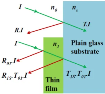
Figure1shows the comparison of light reflection and transmission on a glass substrate with and
without a thin film coating [17]. Here, the incident light is travelling from air to a plain or common
glass substrate (upper portion in Figure1). The intensity of the incident light isI, reflected light is
R.I, and transmitted light isT.I. However, when a thin film coating is added on top of the plain glass
substrate then the light reflection is reduced. Here,Iis the incident light on the coating,R01 is the
reflected light at the interface of air and thin film coating, and transmitted light isT01I. Hence, the
incident light at the coating and glass interface isT01I, transmitted light isT1sT01Iand reflected light is
Energies2016,9, 690 3 of 13
Energies 2016, 9, 690 3 of 13
Figure 1. Comparison of light reflection losses on a plain glass substrate (upper portion: sky blue) by using a thin film on the plain glass substrate (lower portion: light green).
Now, the percentage of light reflection can be calculated by using the following Fresnel equation: 2
0 0
s s
n
n
n
n
R
(1)where, R is the reflection co‐efficient or reflectance, n0 is the refractive index of the first media (here,
it is air), and ns is refractive index of the second media (here, it is glass substrate).
In this situation, if the visible light is travelling from the first media (i.e., air, where n0 = 1.0) to
the second media (i.e., a plain or common glass substrate, where ns = 1.5), the light reflection R is 4%.
However, when a thin film coating is added on the plain or common glass substrate then it (i.e., thin
film coating and the glass together) reduced the reflection losses. The new optimum or equivalent
refractive index, n1 = = √1.0 1.5 = 1.225. The reflection loss of each interface is about 1%.
i.e., the total reflection is about 2%. It was calculated that an intermediate coating between the air and
plain glass substrate can reduce the reflection losses by half (which is about 50%). However, the
formation of an AR coating film can be a complex process and there are several drawbacks, such as
adhesion, thermal mismatch, and instability under thermal cycling [2–4,8].
2.2. Moth’s‐Eye Principle
The versatile visual systems of animals are interesting examples for imagination of nature’s
design. The complex optical concepts evolved as a result of adaptation of different species to their
environment. To identify the innovative applications for modern optics from broad biological
repertoire requires two necessary steps. These are: (i) to understand how a system works; and (ii)
appropriate process technology to reproduce the nature’s design on non‐living matters.
A real example of this concept is the AR surface that found on the eyes of certain butterfly species
in the nature. The compound eyes of these insects are equipped with a periodic array of the SWG
structured bumps. This structure is simply referred to as “moth eye” structure after the moth’s were,
it was observed for the first time, thereby it reduces the light reflection losses, while the transmission
of the chitin‐lens is increased. The evolutionary benefit for the moth is improved vision in a dim
environment while chances to be seen by a predator are lowered.
The idea of SWG structures has been adopted from moths’ eyes principle [8,17]. The surface of
a moth’s eyes is covered with nano‐structured film that absorbs most of the lights instead of reflecting
back as shown in Figure 2. The nano‐structured film consists of a hexagonal pattern bump about 200
nm high, which performs as an AR, because the bumps are smaller than the wavelength of the visible
light. The refractive index between the air and the surface changes gradually, and this gradual change
of refractive index decreases the light reflection. This approach is suitable for solar cells model to
[image:3.595.211.381.87.239.2]reduce the reflection losses and increase the conversion efficiency [2,8,13,15,17].
Figure 1.Comparison of light reflection losses on a plain glass substrate (upper portion: sky blue) by using a thin film on the plain glass substrate (lower portion: light green).
Now, the percentage of light reflection can be calculated by using the following Fresnel equation:
R=
n
0−ns n0+ns
2
(1)
where,Ris the reflection co-efficient or reflectance,n0is the refractive index of the first media (here, it
is air), andnsis refractive index of the second media (here, it is glass substrate).
In this situation, if the visible light is travelling from the first media (i.e., air, wheren0= 1.0) to
the second media (i.e., a plain or common glass substrate, wherens= 1.5), the light reflectionRis 4%.
However, when a thin film coating is added on the plain or common glass substrate then it (i.e., thin film coating and the glass together) reduced the reflection losses. The new optimum or equivalent
refractive index,n1=
√
n0ns=
√
1.0×1.5 = 1.225. The reflection loss of each interface is about 1%. i.e.,
the total reflection is about 2%. It was calculated that an intermediate coating between the air and plain glass substrate can reduce the reflection losses by half (which is about 50%). However, the formation of an AR coating film can be a complex process and there are several drawbacks, such as adhesion, thermal mismatch, and instability under thermal cycling [2–4,8].
2.2. Moth’s-Eye Principle
The versatile visual systems of animals are interesting examples for imagination of nature’s design. The complex optical concepts evolved as a result of adaptation of different species to their environment. To identify the innovative applications for modern optics from broad biological repertoire requires two necessary steps. These are: (i) to understand how a system works; and (ii) appropriate process technology to reproduce the nature’s design on non-living matters.
A real example of this concept is the AR surface that found on the eyes of certain butterfly species in the nature. The compound eyes of these insects are equipped with a periodic array of the SWG structured bumps. This structure is simply referred to as “moth eye” structure after the moth’s were, it was observed for the first time, thereby it reduces the light reflection losses, while the transmission of the chitin-lens is increased. The evolutionary benefit for the moth is improved vision in a dim environment while chances to be seen by a predator are lowered.
The idea of SWG structures has been adopted from moths’ eyes principle [8,17]. The surface of a moth’s eyes is covered with nano-structured film that absorbs most of the lights instead of reflecting
back as shown in Figure2. The nano-structured film consists of a hexagonal pattern bump about
Energies2016,9, 690 4 of 13
Energies 2016, 9, 690 4 of 13
Figure 2. The structure of moth‐eyes which is covered by the nano‐structured film [8,17].
2.3. Subwavelength Grating (SWG) Structure
The subwavelength features have a gradual change in refractive index which acts as a multilayer AR coating leading to a reduced light reflection losses over broadband ranges of wavelength and angle of incidence. The AR coating is an optical coating that is applied to the surface of lenses or any other optical devices to reduce the light reflections. This coating assists the light capturing capacity or improves the efficiency of optical devices, such as lenses or solar cells. Hence, an optimum light reflection can be obtained when the refractive index equates to the square root of the refractive indices of two medium [2]. The multilayer AR coatings can reduce the light reflection losses and increases the conversion efficiency of solar cells.
Figure 3 shows the nano‐grating structures of rectangular and triangular shaped profiles and the plot of SWG structure height versus the effective refractive index (n) for silicon (Si) substrate [16,17]. It shows that for a rectangular‐shaped SWG structure, the refractive index changes very rapidly from air (n = 1.0) to the nano‐structured grating zone (approximately 2.5 at TM mode) [1]. The light reflection loss of a SWG structure can be calculated easily using Fresnel’s equation (which is very similar to the Equation (1)):
2
1 2
1 2
n
n
n
n
R
(2)where, n1 is the refractive index of first medium and n2 is the refractive index of second medium.
Figure 3. Nano‐structured grating of rectangular (or flat type)‐ and triangular (or conical)‐shaped profile,
[image:4.595.150.447.87.246.2]and the plot of SWG height versus the effective refractive index (n) for a silicon (Si) substrate [16,17].
Figure 2.The structure of moth-eyes which is covered by the nano-structured film [8,17].
2.3. Subwavelength Grating (SWG) Structure
The subwavelength features have a gradual change in refractive index which acts as a multilayer AR coating leading to a reduced light reflection losses over broadband ranges of wavelength and angle of incidence. The AR coating is an optical coating that is applied to the surface of lenses or any other optical devices to reduce the light reflections. This coating assists the light capturing capacity or improves the efficiency of optical devices, such as lenses or solar cells. Hence, an optimum light reflection can be obtained when the refractive index equates to the square root of the refractive indices of two medium [2]. The multilayer AR coatings can reduce the light reflection losses and increases the conversion efficiency of solar cells.
Figure3shows the nano-grating structures of rectangular and triangular shaped profiles and the
plot of SWG structure height versus the effective refractive index (n) for silicon (Si) substrate [16,17]. It shows that for a rectangular-shaped SWG structure, the refractive index changes very rapidly from
air (n= 1.0) to the nano-structured grating zone (approximately 2.5 at TM mode) [1]. The light reflection
loss of a SWG structure can be calculated easily using Fresnel’s equation (which is very similar to the Equation (1)):
R=
n2−n1 n2+n1
2
(2)
where,n1is the refractive index of first medium andn2is the refractive index of second medium.
Energies 2016, 9, 690 4 of 13
Figure 2. The structure of moth‐eyes which is covered by the nano‐structured film [8,17].
2.3. Subwavelength Grating (SWG) Structure
The subwavelength features have a gradual change in refractive index which acts as a multilayer
AR coating leading to a reduced light reflection losses over broadband ranges of wavelength and
angle of incidence. The AR coating is an optical coating that is applied to the surface of lenses or any
other optical devices to reduce the light reflections. This coating assists the light capturing capacity
or improves the efficiency of optical devices, such as lenses or solar cells. Hence, an optimum light
reflection can be obtained when the refractive index equates to the square root of the refractive indices
of two medium [2]. The multilayer AR coatings can reduce the light reflection losses and increases
the conversion efficiency of solar cells.
Figure 3 shows the nano‐grating structures of rectangular and triangular shaped profiles and
the plot of SWG structure height versus the effective refractive index (n) for silicon (Si) substrate
[16,17]. It shows that for a rectangular‐shaped SWG structure, the refractive index changes very
rapidly from air (n = 1.0) to the nano‐structured grating zone (approximately 2.5 at TM mode) [1].
The light reflection loss of a SWG structure can be calculated easily using Fresnel’s equation (which
is very similar to the Equation (1)):
2
1 2
1 2
n
n
n
n
R
(2)where, n1 is the refractive index of first medium and n2 is the refractive index of second medium.
Figure 3. Nano‐structured grating of rectangular (or flat type)‐ and triangular (or conical)‐shaped profile,
[image:4.595.176.422.554.733.2]and the plot of SWG height versus the effective refractive index (n) for a silicon (Si) substrate [16,17].
Energies2016,9, 690 5 of 13
From Figure3, the total light reflection from the nano-grating structure can be calculated using
the following equation:
Rtotal=R1+R2 (3)
where,R1is the light reflection at the interface of the air and the grating structure, andR2is the light
reflection at the interface of the grating structure and the substrate.
If the grating structure has a shorter pitch or period than the wavelength of the incident light,
it acts as a homogeneous medium with an effective refractive index [1]. According to Figure3, the
calculated light reflection loss is more than 20.2% for a rectangular-shaped grating structure [1]. For the triangular- or conical-shaped SWG structures, the refractive index changes gradually in several steps, hence the reflection becomes less than 8% [1]. In the parabolic structure, the reflection loss is lower than the rectangular-shaped grating structure but higher than that the triangular-shaped grating structure (about 5%) [14].
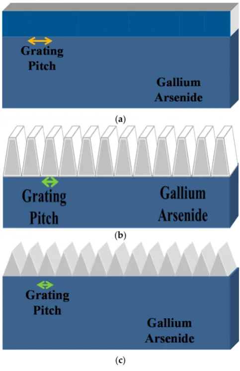
3. Geometric Shape Design of Nano-Gratings
This section briefly discussed the geometric shape design of nano-grating structure on the GaAs
substrates. The SWG structures are namely; (i) rectangular-shaped SWG (as shown in Figure4c);
(ii) trapezoidal-shaped SWG with different aspect ratios (i.e., 0.1, 0.2, 0.5, 0.8, and 0.9) as shown in
Figure4b; and (iii) triangular-shaped SWG (as shown in Figure4a).
Energies 2016, 9, 690 5 of 13
From Figure 3, the total light reflection from the nano‐grating structure can be calculated using the following equation:
2 1
R
R
R
total
(3)where, R1 is the light reflection at the interface of the air and the grating structure, and R2 is the light
reflection at the interface of the grating structure and the substrate.
If the grating structure has a shorter pitch or period than the wavelength of the incident light, it acts as a homogeneous medium with an effective refractive index [1]. According to Figure 3, the calculated light reflection loss is more than 20.2% for a rectangular‐shaped grating structure [1]. For the triangular‐ or conical‐shaped SWG structures, the refractive index changes gradually in several steps, hence the reflection becomes less than 8% [1]. In the parabolic structure, the reflection loss is lower than the rectangular‐shaped grating structure but higher than that the triangular‐shaped grating structure (about 5%) [14].
3. Geometric Shape Design of Nano‐Gratings
This section briefly discussed the geometric shape design of nano‐grating structure on the GaAs substrates. The SWG structures are namely; (i) rectangular‐shaped SWG (as shown in Figure 4c); (ii) trapezoidal‐shaped SWG with different aspect ratios (i.e., 0.1, 0.2, 0.5, 0.8, and 0.9) as shown in Figure 4b; and (iii) triangular‐shaped SWG (as shown in Figure 4a).
(a) (b) (c)
Figure 4. Geometric shape design of nano‐grating structures those are used in the simulations.
(a) triangular‐shaped SWG; (b) trapezoidal‐shaped SWG; and (c) rectangular‐shaped SWG.
The term aspect ratio (AspR) is defined as the ratio between the top length over the base length of a trapezoid, triangle, and/or rectangle [5,6,14,16,17]. It is clear from Figure 5 that the AspR can be written as follows:
b
a
AspR
(4)where, “a” is the top length and “b” is the base length of the geometric shapes (such as, triangle, trapezoid, and rectangle). For a rectangular‐shaped nano‐grating profile, the AspR is ‘1’ (i.e., the top and base length of the rectangle is equal) and for the triangular‐shaped nano‐grating profile, the AspR is ‘0’ (i.e., the top length of the triangle is ‘0’ compared to the base length of the triangle). However, for a trapezoidal‐shaped nano‐grating the AspR is 0 < (a/b) < 1, i.e., it lies between ‘0’ to ‘1’ (such as, 0.1–0.9.). These nano‐grating shapes play an important role for the light trapping inside the substrate that affect on the conversion efficiency of solar cells. Therefore, the design of nano‐grating structures is essential to reduce the light reflection losses and improve the conversion efficiency in GaAs solar cells. In the next section, the design of nano‐grating structures is discussed briefly.
4. Design of Nano‐Grating Structures
This section discussed about the nano‐gratings shape design and modeling of nano‐gratings structures (i.e., SWG structures). The light reflection is strongly dependent on the nano‐grating structures; therefore, an appropriate design of nano‐grating structure is important and essential to
Figure 4. Geometric shape design of nano-grating structures those are used in the simulations. (a) triangular-shaped SWG; (b) trapezoidal-shaped SWG; and (c) rectangular-shaped SWG.
The term aspect ratio (AspR) is defined as the ratio between the top length over the base length
of a trapezoid, triangle, and/or rectangle [5,6,14,16,17]. It is clear from Figure5that theAspRcan be
written as follows:
AspR= a
b (4)
where, “a” is the top length and “b” is the base length of the geometric shapes (such as, triangle,
trapezoid, and rectangle). For a rectangular-shaped nano-grating profile, theAspRis ‘1’ (i.e., the top
and base length of the rectangle is equal) and for the triangular-shaped nano-grating profile, theAspR
is ‘0’ (i.e., the top length of the triangle is ‘0’ compared to the base length of the triangle). However,
for a trapezoidal-shaped nano-grating theAspRis 0 < (a/b) < 1, i.e., it lies between ‘0’ to ‘1’ (such as,
0.1–0.9.). These nano-grating shapes play an important role for the light trapping inside the substrate that affect on the conversion efficiency of solar cells. Therefore, the design of nano-grating structures is essential to reduce the light reflection losses and improve the conversion efficiency in GaAs solar cells. In the next section, the design of nano-grating structures is discussed briefly.
4. Design of Nano-Grating Structures
Energies2016,9, 690 6 of 13
model for reduction of reflection losses of light. For this reason, the nano-grating shapes are designed and optimized to reduce the light reflection losses from the surface of the GaAs solar cells or panels. The modeled nano-structured gratings are: (i) rectangular-shaped nano-grating profile (as shown
in Figure5a); (ii) trapezoidal-shaped nano-grating profile with different aspect ratios of 0.1–0.9 (as
shown in Figure5b); and (iii) triangular-shaped nano-grating profile (as shown in Figure5c). Here,
we discussed all these nano-grating shapes as shown in Figure 5a–c. For the rectangular-shaped
nano-grating profile, the aspect ratio is ‘1’ (i.e., the top and base length of the trapezoid is equal), for trapezoidal-shaped nano-grating profile, the aspect ratio varies from ‘0.1–0.9’ (i.e., it depends on the top length of the trapezoid), and for the triangular-shaped nano-grating profile, the aspect ratio is ‘0’ (i.e., the top length of the trapezoid is zero compared to the base length of the trapezoid). These shapes are used for the simulation and analyzed the results for light reflection of the SWG structures [5,6,14,16,17].
Energies 2016, 9, 690 6 of 13
model for reduction of reflection losses of light. For this reason, the nano‐grating shapes are designed and optimized to reduce the light reflection losses from the surface of the GaAs solar cells or panels. The modeled nano‐structured gratings are: (i) rectangular‐shaped nano‐grating profile (as shown in Figure 5a); (ii) trapezoidal‐shaped nano‐grating profile with different aspect ratios of 0.1–0.9 (as shown in Figure 5b); and (iii) triangular‐shaped nano‐grating profile (as shown in Figure 5c). Here, we discussed all these nano‐grating shapes as shown in Figure 5a–c. For the rectangular‐shaped nano‐grating profile, the aspect ratio is ‘1’ (i.e., the top and base length of the trapezoid is equal), for trapezoidal‐shaped nano‐grating profile, the aspect ratio varies from ‘0.1–0.9’ (i.e., it depends on the top length of the trapezoid), and for the triangular‐shaped nano‐grating profile, the aspect ratio is ‘0’ (i.e., the top length of the trapezoid is zero compared to the base length of the trapezoid). These shapes are used for the simulation and analyzed the results for light reflection of the SWG structures [5,6,14,16,17].
(a)
(b)
(c)
Figure 5. Nano‐grating profiles for the simulation of light reflection in GaAs solar cells: (a)
rectangular‐shaped nano‐grating profile; (b) trapezoidal‐shaped nano‐grating profile; and (c)
triangular‐ or conical‐shaped nano‐grating profile. Here, the nano‐gratings and substrate are gallium
arsenide (GaAs).
5. Nano‐Structures Simulation by FDTD
The Optiwave FDTD (OptiFDTD) simulation tool is a very powerful, highly‐integrated software that allows computer aided design and advanced simulation of passive photonic components.
[image:6.595.176.418.260.633.2]The FDTD method is an intuitive way to solve the partial differential equations numerically [19]. It is a simple method utilizes the central difference approximation to discretize the two Maxwell’s
Figure 5.Nano-grating profiles for the simulation of light reflection in GaAs solar cells: (a) rectangular-shaped nano-grating profile; (b) trapezoidal-shaped nano-grating profile; and (c) triangular- or conical-shaped nano-grating profile. Here, the nano-gratings and substrate are gallium arsenide (GaAs).
5. Nano-Structures Simulation by FDTD
The Optiwave FDTD (OptiFDTD) simulation tool is a very powerful, highly-integrated software that allows computer aided design and advanced simulation of passive photonic components.
Energies2016,9, 690 7 of 13
curl equations, namely, Faraday’s and Ampere’s laws, both in time and spatial domains, and then it solves the resulting equations numerically to derive the electric and magnetic field distributions at each time step using an explicit leapfrog scheme. The FDTD solution, thus derived, is second-order accurate, and is stable if the time step satisfies the Courant condition. One of the most important attributes of the FDTD algorithm is that it is appropriately parallel in nature, i.e., parallel processing in both the time and spatial domains, because it only requires exchange of information at the interfaces of the sub-domains in the parallel processing scheme, which consequently makes it faster and more efficient [20].
The OptiFDTD software package is based on the FDTD algorithm was originally proposed by K. S. Yee in 1966 [21,22]. It introduced a modeling technique with second order central differences to solve the Maxwell equations applying a finite difference approach (or mathematics). The FDTD algorithm can directly calculate the value of E (electric field intensity) and H (magnetic field intensity) at different points of the computational domain. Since then, it has been used for several applications and many extensions of the basic algorithm have been developed [22–28].
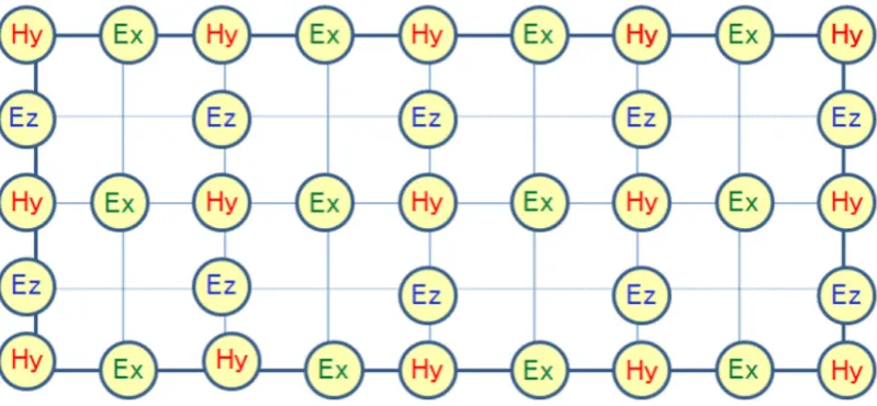
In the two-dimensional (2D) FDTD simulation for TM wave (Ex,Hy,Ez—nonzero components,
propagation along withZ, transverse field variations along withX) in lossless media, Maxwell's
equations take the following form:
∂Hy
∂t =−
1 µ0
∂Ex
∂z −
∂Ez ∂x
, ∂Ex
∂t =
1 µ0
∂Hy ∂z ,
∂Ez
∂t =
1 ε
∂Hy
∂x (5)
The location of the TM fields in the computational domain (mesh) follows the same philosophy
as shown in the following Figure6.
Energies 2016, 9, 690 7 of 13
curl equations, namely, Faraday’s and Ampere’s laws, both in time and spatial domains, and then it
solves the resulting equations numerically to derive the electric and magnetic field distributions at
each time step using an explicit leapfrog scheme. The FDTD solution, thus derived, is second‐order
accurate, and is stable if the time step satisfies the Courant condition. One of the most important
attributes of the FDTD algorithm is that it is appropriately parallel in nature, i.e., parallel processing
in both the time and spatial domains, because it only requires exchange of information at the
interfaces of the sub‐domains in the parallel processing scheme, which consequently makes it faster
and more efficient [20].
The OptiFDTD software package is based on the FDTD algorithm was originally proposed by
K. S. Yee in 1966 [21,22]. It introduced a modeling technique with second order central differences to
solve the Maxwell equations applying a finite difference approach (or mathematics). The FDTD
algorithm can directly calculate the value of E (electric field intensity) and H (magnetic field intensity)
at different points of the computational domain. Since then, it has been used for several applications
and many extensions of the basic algorithm have been developed [22–28].
In the two‐dimensional (2D) FDTD simulation for TM wave (Ex, Hy, Ez—nonzero components, propagation along with Z, transverse field variations along with X) in lossless media, Maxwellʹs
equations take the following form:
0 0
1
1
1
,
,
μ
μ
ε
y x z x y z y
H
E
E
E
H
E
H
t
z
x
t
z
t
x
(5)The location of the TM fields in the computational domain (mesh) follows the same philosophy
as shown in the following Figure 6.
Figure 6. Basic numerical simulation of a 2D computational domain of FDTD software for nano‐
grating structures. The detail location of TM fields in the computational domain.
Figure 6 shows the basic numerical representation of a 2D computational domain of OptiFDTD
software for nano‐grating structures simulation. Now, the electric field components Ex and Ez are associated with the cell edges, while the magnetic field Hy is located at the center of the cell.
6. Simulation Results and Discussion
In this section, we discussed the simulation results of SWG structures. The simulation results
obtained by using the OptiFDTD software package, which is based on the FDTD method that was
developed by Optiwave Inc. (Ottawa, ON, Canada) [22]. This FDTD software gives numerical
solutions by using Maxwell’s equation.
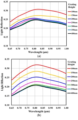
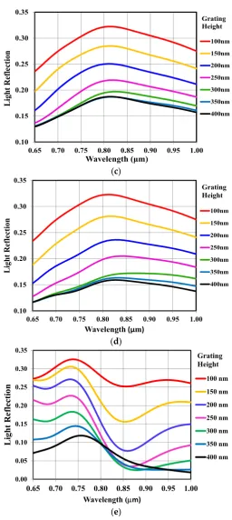
The FDTD simulation tool is used to calculate the light reflection losses of SWG structures (here,
GaAs solar cells) for conversion efficiency improvement. The nano‐grating pitch or period and height
[image:7.595.100.500.396.581.2]of the SWG structures were varied to realize the minimum reflection losses in GaAs solar cells. Figure Figure 6.Basic numerical simulation of a 2D computational domain of FDTD software for nano-grating structures. The detail location of TM fields in the computational domain.
Figure6shows the basic numerical representation of a 2D computational domain of OptiFDTD
software for nano-grating structures simulation. Now, the electric field componentsExandEzare
associated with the cell edges, while the magnetic fieldHyis located at the center of the cell.
6. Simulation Results and Discussion
Energies2016,9, 690 8 of 13
The FDTD simulation tool is used to calculate the light reflection losses of SWG structures (here, GaAs solar cells) for conversion efficiency improvement. The nano-grating pitch or period and height
of the SWG structures were varied to realize the minimum reflection losses in GaAs solar cells. Figure7
shows the light reflection losses spectra for several nano-grating heights (such as, the heights are varied from 100 nm to 400 nm) with different pitches or periods. The pitches or periods for this simulation
are: (Figure7a) 200 nm, (7b) 300 nm, (7c) 350 nm, (7d) 400 nm, and (7e) 830 nm. For this simulation,
the incident light wavelength was kept constant at 830 nm. The simulated results show that with the increase of nano-grating heights, the light reflection reduces and reached to the saturation of light reflection at 300 nm. In this case, the nano-grating height about 300 nm has the minimum light reflection losses for GaAs solar cells. This is due to the saturation of the nano-grating’s height for this specific design. Hence, this results confirm that when the nano-grating height is about 300 nm the light reflection loss is minimum. It has also been observed that the light reflection for 300 nm and 350 nm nano-grating height is very close. This nano-grating height for light reflection is minimum and it is saturated, which is the similar tendency as reported in [3]. When the nano-grating height increases further, such as the nano-grating height is 400 nm, the light reflection again increases as shown in
Figure7. It has again confirmed from the Figure8. The light reflection versus nano-grating height is
plotted in Figure8using the data of Figure7e when the nano-grating pitch or period is 830 nm.
Energies 2016, 9, 690 8 of 13
7 shows the light reflection losses spectra for several nano‐grating heights (such as, the heights are
varied from 100 nm to 400 nm) with different pitches or periods. The pitches or periods for this
simulation are: (Figure 7a) 200 nm, (7b) 300 nm, (7c) 350 nm, (7d) 400 nm, and (7e) 830 nm. For this
simulation, the incident light wavelength was kept constant at 830 nm. The simulated results show
that with the increase of nano‐grating heights, the light reflection reduces and reached to the
saturation of light reflection at 300 nm. In this case, the nano‐grating height about 300 nm has the
minimum light reflection losses for GaAs solar cells. This is due to the saturation of the nano‐grating’s
height for this specific design. Hence, this results confirm that when the nano‐grating height is about
300 nm the light reflection loss is minimum. It has also been observed that the light reflection for 300
nm and 350 nm nano‐grating height is very close. This nano‐grating height for light reflection is
minimum and it is saturated, which is the similar tendency as reported in [3]. When the nano‐grating
height increases further, such as the nano‐grating height is 400 nm, the light reflection again increases
as shown in Figure 7. It has again confirmed from the Figure 8. The light reflection versus nano‐
grating height is plotted in Figure 8 using the data of Figure 7e when the nano‐grating pitch or period
is 830 nm.
(a)
(b)
0.10 0.15 0.20 0.25 0.30 0.35
0.65 0.70 0.75 0.80 0.85 0.90 0.95 1.00
Li
gh
t R
efl
ect
io
n
Wavelength (μm)
100nm 150nm 200nm 250nm 300nm 350nm 400nm Grating Height
0.10 0.15 0.20 0.25 0.30 0.35
0.65 0.70 0.75 0.80 0.85 0.90 0.95 1.00
Li
gh
t R
flect
ion
Wavelength (μm)
100nm 150nm 200nm 250nm
[image:8.595.169.424.331.724.2]300nm 350nm 400nm Grating Height
Energies2016,9, 690 9 of 13
Energies 2016, 9, 690 9 of 13
(c)
(d)
(e)
Figure 7. Light reflection spectra for several triangular‐ or conical‐shaped nano‐grating heights with
different pitch or period. The periods are: (a) triangular‐ or conical‐shaped nano‐grating with pitch
200 nm; (b) triangular‐ or conical‐shaped nano‐grating with pitch 300 nm; (c) triangular‐ or conical‐
shaped nano‐grating with a pitch 350 nm; (d) triangular‐ or conical‐shaped nano‐grating with pitch
400 nm; and (e) triangular‐ or conical‐shaped nano‐grating with pitch 830 nm. The incident light
wavelength is kept constant at 830 nm.
0.10 0.15 0.20 0.25 0.30 0.35
0.65 0.70 0.75 0.80 0.85 0.90 0.95 1.00
Lig
ht R
efl
ecti
on
Wavelength (μm)
100nm 150nm 200nm
250nm 300nm 350nm 400nm Grating Height
0.10 0.15 0.20 0.25 0.30 0.35
0.65 0.70 0.75 0.80 0.85 0.90 0.95 1.00
Li
gh
t Re
fl
ec
ti
on
Wavelength(μm)
100nm
150nm
200nm
250nm
300nm
350nm
400nm Grating Height
0.00 0.05 0.10 0.15 0.20 0.25 0.30 0.35
0.65 0.70 0.75 0.80 0.85 0.90 0.95 1.00
Light Re
fl
ec
tion
Wavelength (m)
100 nm
150 nm
200 nm 250 nm
300 nm
[image:9.595.170.427.82.656.2]350 nm 400 nm Grating Height
Energies2016,9, 690 10 of 13
Energies 2016, 9, 690 10 of 13
Figure 8. Light reflection versus nao‐grating height characteristics when the grating pitch or period
is kept constant at 830 nm.
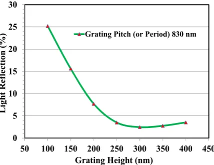
Figure 8 shows the simulated minimum light reflection versus the nano‐grating height
characteristics for a triangular (i.e., conical or perfect cone)‐shaped nano‐grating structure of GaAs
having a constant period at 830 nm. The minimum light reflection about 2% was observed at 300 nm
nano‐grating height. However, when the nano‐grating heights further increased to 350 nm and 400
nm, then the light reflection increased further to higher order direction, such as about 4%. Therefore,
this results indicated that the nano‐grating height about 300 nm has the minimum reflection losses
for GaAs solar cells. This simulated results confirmed that the nano‐grating height about 300 nm is
the optimum nano‐grating height for minimum light reflection losses of GaAs solar cells. Hence, most
of the incident light passes through the GaAs substrate without reflecting back to the air (i.e., reduced
the light reflection losses) and it increases the conversion efficiency of GaAs solar cells significantly.
For minimum light reflection, we have considered different aspect ratio’s for the nano‐grating
period or pitches of 830‐nm to obtain the minimum light reflection for GaAs solar cells structure. The
parameter “aspect ratio” controls the shape of the nano‐grating structure. Figure 9 shows the
minimum light reflection loss for the nano‐grating pitch (or period) of 830 nm. For this case, the
minimum light reflection is approximately 1%–2% with the nano‐grating height of 300–400 nm, when
the aspect ratio is ‘0’. However, the light reflection is increased to 1%–4% (with the aspect ratio of 0.5)
and the nano‐grating height of 250–450 nm; and reaches to 13%–17% with the aspect ratio of 0.8 and
the nano‐grating height of 200–450 nm.
Figure 9. Minimum light reflection versus the nano‐grating height characteristics with the grating
period or pitch of 830 nm. Here, the aspect ratio is considered “0” as triangular‐shaped nano‐grating,
“0.5” and “0.8” as the trapezoidal‐shaped nano‐grating.
Figure 10 shows the minimum light reflection versus the aspect ratio characteristics for different
nano‐grating heights. For this study, the nano‐grating height is varied from 50 nm to 500 nm. For this 0 5 10 15 20 25 30
50 100 150 200 250 300 350 400 450
Ligh t R eflec tion ( % )
Grating Height (nm)
[image:10.595.191.406.89.254.2]Grating Pitch (or Period) 830 nm
Figure 8.Light reflection versus nao-grating height characteristics when the grating pitch or period is kept constant at 830 nm.
Figure 8 shows the simulated minimum light reflection versus the nano-grating height
characteristics for a triangular (i.e., conical or perfect cone)-shaped nano-grating structure of GaAs having a constant period at 830 nm. The minimum light reflection about 2% was observed at 300 nm nano-grating height. However, when the nano-grating heights further increased to 350 nm and 400 nm, then the light reflection increased further to higher order direction, such as about 4%. Therefore, this results indicated that the nano-grating height about 300 nm has the minimum reflection losses for GaAs solar cells. This simulated results confirmed that the nano-grating height about 300 nm is the optimum nano-grating height for minimum light reflection losses of GaAs solar cells. Hence, most of the incident light passes through the GaAs substrate without reflecting back to the air (i.e., reduced the light reflection losses) and it increases the conversion efficiency of GaAs solar cells significantly.
For minimum light reflection, we have considered different aspect ratio’s for the nano-grating period or pitches of 830-nm to obtain the minimum light reflection for GaAs solar cells structure.
The parameter “aspect ratio” controls the shape of the nano-grating structure. Figure9shows the
minimum light reflection loss for the nano-grating pitch (or period) of 830 nm. For this case, the minimum light reflection is approximately 1%–2% with the nano-grating height of 300–400 nm, when the aspect ratio is ‘0’. However, the light reflection is increased to 1%–4% (with the aspect ratio of 0.5) and the nano-grating height of 250–450 nm; and reaches to 13%–17% with the aspect ratio of 0.8 and the nano-grating height of 200–450 nm.
Energies 2016, 9, 690 10 of 13
Figure 8. Light reflection versus nao‐grating height characteristics when the grating pitch or period
is kept constant at 830 nm.
Figure 8 shows the simulated minimum light reflection versus the nano‐grating height characteristics for a triangular (i.e., conical or perfect cone)‐shaped nano‐grating structure of GaAs having a constant period at 830 nm. The minimum light reflection about 2% was observed at 300 nm nano‐grating height. However, when the nano‐grating heights further increased to 350 nm and 400 nm, then the light reflection increased further to higher order direction, such as about 4%. Therefore, this results indicated that the nano‐grating height about 300 nm has the minimum reflection losses for GaAs solar cells. This simulated results confirmed that the nano‐grating height about 300 nm is the optimum nano‐grating height for minimum light reflection losses of GaAs solar cells. Hence, most of the incident light passes through the GaAs substrate without reflecting back to the air (i.e., reduced the light reflection losses) and it increases the conversion efficiency of GaAs solar cells significantly.
For minimum light reflection, we have considered different aspect ratio’s for the nano‐grating period or pitches of 830‐nm to obtain the minimum light reflection for GaAs solar cells structure. The parameter “aspect ratio” controls the shape of the nano‐grating structure. Figure 9 shows the minimum light reflection loss for the nano‐grating pitch (or period) of 830 nm. For this case, the minimum light reflection is approximately 1%–2% with the nano‐grating height of 300–400 nm, when the aspect ratio is ‘0’. However, the light reflection is increased to 1%–4% (with the aspect ratio of 0.5) and the nano‐grating height of 250–450 nm; and reaches to 13%–17% with the aspect ratio of 0.8 and the nano‐grating height of 200–450 nm.
Figure 9. Minimum light reflection versus the nano‐grating height characteristics with the grating
period or pitch of 830 nm. Here, the aspect ratio is considered “0” as triangular‐shaped nano‐grating,
“0.5” and “0.8” as the trapezoidal‐shaped nano‐grating.
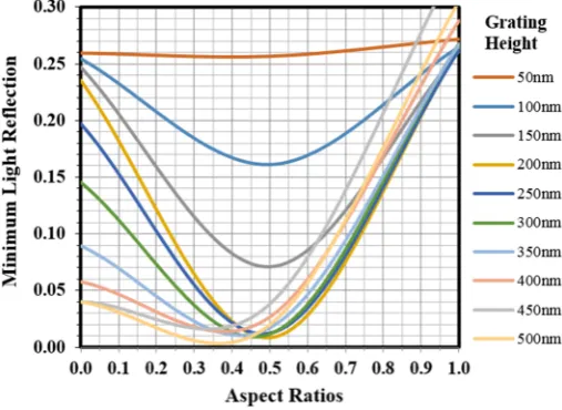
Figure 10 shows the minimum light reflection versus the aspect ratio characteristics for different nano‐grating heights. For this study, the nano‐grating height is varied from 50 nm to 500 nm. For this
0 5 10 15 20 25 30
50 100 150 200 250 300 350 400 450
Ligh t R eflec tion ( % )
Grating Height (nm)
[image:10.595.188.409.565.716.2]Grating Pitch (or Period) 830 nm
Energies2016,9, 690 11 of 13
Figure10shows the minimum light reflection versus the aspect ratio characteristics for different
nano-grating heights. For this study, the nano-grating height is varied from 50 nm to 500 nm. For this case, the nano-grating period is kept constant at 830 nm. Here, the aspect ratio is varied from ‘0’ to ‘1’. As discussed earlier, when the aspect ratio is ‘0’ then the shape of the nano-grating is triangular and when the aspect ratio is >0 but <1, then the shape of the nano-grating is trapezoidal. However, when the aspect ratio is ‘1’ then the shape of the nano-grating is rectangular. The simulated results show the light reflection for 50 nm grating height is >26%, which is like a flat type (about 30% light reflection) substrates. From the plot, it shows clearly that when the nano-grating height increasing from 50 nm to 250–350 nm, then the light reflection is decreasing sharply and drops to about 2%. However, if further increasing the nano-grating height, the reflection loss is increasing rapidly and reached toward to the flat type of substrates, like a 50 nm nano-grating height.
Energies 2016, 9, 690 11 of 13
case, the nano‐grating period is kept constant at 830 nm. Here, the aspect ratio is varied from ‘0’ to
‘1’. As discussed earlier, when the aspect ratio is ‘0’ then the shape of the nano‐grating is triangular
and when the aspect ratio is >0 but <1, then the shape of the nano‐grating is trapezoidal. However,
when the aspect ratio is ‘1’ then the shape of the nano‐grating is rectangular. The simulated results
show the light reflection for 50 nm grating height is >26%, which is like a flat type (about 30% light
reflection) substrates. From the plot, it shows clearly that when the nano‐grating height increasing
from 50 nm to 250–350 nm, then the light reflection is decreasing sharply and drops to about 2%.
However, if further increasing the nano‐grating height, the reflection loss is increasing rapidly and
reached toward to the flat type of substrates, like a 50 nm nano‐grating height.
Figure 10. Minimum light reflection versus the aspect ratios for different nano‐grating heights with
the grating period or pitch of 830‐nm. Here, the nano‐grating height is varied from 50 nm to 500 nm.
7. Conclusions
In conclusion, this paper reported the design and analysis of nano‐structured gratings that can
improve the conversion efficiency in GaAs solar cells. The light reflection is about 2% with an
optimized nano‐grating height of about 300 nm and the period of about 830 nm, which is about 28%
lower than that of flat type substrates. The light reflection is calculated by the FDTD simulation tool.
The simulated results confirm that the light reflection of a rectangular‐shaped nano‐grating structure
is about 30%, however, the light reflection becomes about 2% for a triangular (i.e., conical or perfect
cone)‐shaped nano‐grating structure, because the refractive index changes gradually in several steps
and reduces the light reflection losses from the surface of the substrates or panels. From the
simulations, it also noticed that the intermediate structures (i.e., trapezoidal‐ and parabolic‐shaped),
the light reflection loss is lower than the rectangular shaped nano‐grating structure but higher than
the triangular‐shaped nano‐grating structure. The simulated results confirm that the reduction of
light reflection losses will increase the conversion efficiency significantly in GaAs solar cells can be
correlated to a practical example of higher conversion efficiency achieved in thin layer dielectric‐
coated graphene/GaAs solar cells [12]. Therefore, it has confirmed that the triangular (i.e., conical or
perfect cone)‐shaped nano‐grating structures are an excellent alternative antireflective (AR) coating
for the reduction of light reflection losses and improve the conversion efficiency in GaAs solar cells
for a sustainable future.
Acknowledgments: This research is supported by the Centre for Smart Grid and Sustainable Power Systems,
the Faculty of Science and Engineering, Curtin University, Perth, Australia and School of Mechanical and
Electrical Engineering, Faculty of Health, Engineering, and Sciences, University of Southern Queensland,
Toowoomba, Australia.
Author Contributions: Narottam Das and Syed Islam conceived, designed and performed the simulations,
analyzed the data/results and wrote the paper.
Figure 10.Minimum light reflection versus the aspect ratios for different nano-grating heights with the grating period or pitch of 830-nm. Here, the nano-grating height is varied from 50 nm to 500 nm.
7. Conclusions
In conclusion, this paper reported the design and analysis of nano-structured gratings that can improve the conversion efficiency in GaAs solar cells. The light reflection is about 2% with an optimized nano-grating height of about 300 nm and the period of about 830 nm, which is about 28% lower than that of flat type substrates. The light reflection is calculated by the FDTD simulation tool. The simulated results confirm that the light reflection of a rectangular-shaped nano-grating structure is about 30%, however, the light reflection becomes about 2% for a triangular (i.e., conical or perfect cone)-shaped nano-grating structure, because the refractive index changes gradually in several steps and reduces the light reflection losses from the surface of the substrates or panels. From the simulations, it also noticed that the intermediate structures (i.e., trapezoidal- and parabolic-shaped), the light reflection loss is lower than the rectangular shaped nano-grating structure but higher than the triangular-shaped nano-grating structure. The simulated results confirm that the reduction of light reflection losses will increase the conversion efficiency significantly in GaAs solar cells can be correlated to a practical example of higher conversion efficiency achieved in thin layer dielectric-coated graphene/GaAs solar cells [12]. Therefore, it has confirmed that the triangular (i.e., conical or perfect cone)-shaped nano-grating structures are an excellent alternative antireflective (AR) coating for the reduction of light reflection losses and improve the conversion efficiency in GaAs solar cells for a sustainable future.
[image:11.595.171.425.251.436.2]Energies2016,9, 690 12 of 13
Author Contributions: Narottam Das and Syed Islam conceived, designed and performed the simulations, analyzed the data/results and wrote the paper.
Conflicts of Interest:The authors declare no conflict of interest.
References
1. Song, Y.M.; Lee, Y.T. Simulation of antireflective subwavelength grating structure for optical device
applications. In Proceedings of the 9th International Conference on Numerical Simulations of Optoelectronic Devices 2009 (NUSOD’09), Gwangju, Korea, 14–17 September 2009; pp. 103–104.
2. Schmid, J.H.; Cheben, P.; Janz, S.; Lapointe, J.; Post, E.; Delage, A.; Densmore, A.; Lamontagne, B.;
Waldron, P.; Xu, D.-X. Subwavelength grating structures in planar waveguide facets for modified reflectivity. In Proceedings of the SPIE—The International Society for Optical Engineering, Ottawa, ON, Canada, 4 June 2007; Volume 6796.
3. Sikder, U.; Zaman, M.A. Optimization of multilayer antireflection coating for photovoltaic applications.
Opt. Laser Technol.2016,79, 88–94. [CrossRef]
4. Bouhafs, D.; Moussi, A.; Chikouche, A.; Ruiz, J. Design and simulation of antireflection coating systems for optoelectronic devices: Application to silicon solar cells. Sol. Energy Mater. Sol. Cells1998,52, 79–93. [CrossRef]
5. Das, N.K.; Tan, C.L.; Lysak, V.V.; Alameh, K.; Lee, Y.T. Light absorption enhancement in metal-semiconductor-metal
photodetectors using plasmonic nanostructure gratings. In Proceedings of the 6th International
Symposium on High capacity Optical Networks and Enabling Technologies, HONET’09, Alexandria, Egypt, 28–30 December 2009; pp. 86–90.
6. Das, N.; Karar, A.; Vasiliev, M.; Tan, C.L.; Alameh, K.; Lee, Y.T. Analysis of nano-grating assisted
light absorption enhancement in metal-semiconductor-metal photodetectors patterned using focused ion beam lithography.Opt. Commun.2011,284, 1694–1700. [CrossRef]
7. Ko, H.D. Surface Plasmon Coupled Sensor and Nanolens. Ph.D. Thesis, Texas A&M University,
College Station, TX, USA, 2009.
8. Lee, Y.T. High-efficiency GaInP/LCM-GaInP/GaAs triple-junction solar cells with antireflective subwavelength structures. In Proceedings of the Pioneering Symposium (PC-02), Gwangu, Korea, October 2009.
9. Udagedara, I.B.; Rukhlenko, I.D.; Premaratne, M. Surface plasmon-polariton propagation in piecewise
linear chains of composite nanospheres: The role of optical gain and chain layout. Opt. Express2011,19, 19973–19986. [CrossRef] [PubMed]
10. Rukhlenko, I.D.; Pannipitiya, A.; Premaratne, M. Dispersion relation for surface plasmon polaritons in
metal/nonlinear-dielectric/metal slot waveguides.Opt. Lett.2011,36, 3374–3376. [CrossRef] [PubMed]
11. Zhu, W.; Rukhlenko, I.D.; Premaratne, M. Graphene metamaterial for optical reflection modulation.
Appl. Phys. Lett.2013,102, 241914. [CrossRef]
12. Li, X.; Zhang, S.; Wang, P.; Zhong, H.; Wu, Z.; Chen, H.; Li, E.; Liu, C.; Lin, S. High performance solar cells based on graphene/GaAs hetero-structures.Nano Energy2015,16, 310. [CrossRef]
13. Thelen, A.Design of Optical Interference Coatings; McGraw-Hill: New York, NY, USA, 1989.
14. Sahoo, K.C.; Li, Y.; Chang, E.Y. Shape effect of silicon nitride subwavelength structure on reflectance for silicon solar cells.IEEE Trans. Electron. Device2010,57, 2427–2433. [CrossRef]
15. Song, Y.M.; Jang, S.J.; Yu, J.S.; Lee, Y.T. Bioinspired parabola subwavelength structures for improved
broadband antireflection.Small2010,6, 984–987. [CrossRef] [PubMed]
16. Moushumy, N.; Das, N.K.; Alameh, K.; Lee, Y.T. Design and development of silver nanoparticles to reduce the reflection loss of solar cell. In Proceedings of the 8th International Conference on High-capacity Optical Networks and Emerging Technologies (HONET’11), Riyadh, Saudi Arabia, 19–21 December 2011; pp. 38–41.
17. Das, N.K.; Islam, S.M. Optimization of nano-grating structure to reduce the reflection losses in GaAs
solar cells. In Proceedings of the Australasian Universities Power Engineering Conference 2012 (AUPEC 2012), Denpasar-Bali, Indonesia, 26–29 September 2012.
18. Bondeson, A.; Rylander, T.; Ingelstrom, P.Computational Electromagnetics, 1st ed.; Springer: New York, NY, USA, 2005.
Energies2016,9, 690 13 of 13
20. Yu, W.Electromagnetic Simulation Techniques Based on the FDTD Method; John Wiley & Sons: Hoboken, NJ, USA, 2009.
21. Yee, K.S. Numerical solution of initial boundary value problems involving Maxwell’s equations in
isotropic media.IEEE Trans. Antennas Propag.1966,14, 302–307.
22. Optiwave Support Team.Finite Difference Time Domain Photonics Simulation Software; OptiFDTD Technical background and Tutorials, Version 8; Optiwave System Inc.: Ottawa, ON, Canada, 2008.
23. Raki´c, A.D.; Djuriši´c, A.B.; Elazar, J.M.; Majewski, M.L. Optical properties of metallic films for vertical-cavity optoelectronic devices.Appl. Opt.1998,37, 5271–5283. [CrossRef] [PubMed]
24. Markovic, M.I.; Rakic, A.D. Determination of reflection coefficients of laser light of wavelength from the surface of aluminum using the Lorentz-Drude model.Appl. Opt.1990,29, 3479–3483. [CrossRef] [PubMed] 25. Markovic, M.I.; Rakic, A.D. Determination of optical properties of aluminum including electron reradiation
in the Lorentz-Drude Model.Opt. Laser Technol.1990,22, 394–398. [CrossRef]
26. Dhakal, D. Analysis of the Sub-Wavelength Grating in OptiFDTD Simulator. Master’s Thesis, Jacobs University, Bremen, Germany, 2009.
27. Ferry, V.E.; Sweatlock, L.A.; Pacifici, D.; Atwater, H.A. Plasmonic nanostructure design for efficient light coupling into solar cells.Nano Lett.2008,8, 4391–4397. [CrossRef] [PubMed]
28. Kabir, M.I.; Ibrahim, Z.; Sopian, K.; Amin, N. Effect of structural variations in amorphous silicon based single and multi-junction solar cells from numerical analysis.Sol. Energy Mater. Sol. Cells2010,95, 1542–1545. [CrossRef]
![Figure 2.Figure The structure of moth-eyes which is covered by the nano-structured film [2. The structure of moth‐eyes which is covered by the nano‐structured film [8,17].8,17 ].](https://thumb-us.123doks.com/thumbv2/123dok_us/146710.23854/4.595.150.447.87.246/figure-figure-structure-covered-structured-structure-covered-structured.webp)