Electrically-Tunable
Light-Matter Interactions
in Quantum Materials
Thesis by
William Schuyler Whitney
In Partial Fulfillment of the Requirements for
the degree of
Doctor of Philosophy
CALIFORNIA INSTITUTE OF TECHNOLOGY
Pasadena, California
2019
2019
Acknowledgements
To start, I would like to acknowledge everyone who encouraged me to find my way to
Caltech. As an undergraduate with no lab experience, Professor Eric Mazur at Harvard
was kind enough to let me join his research group for a summer, and learn from his
students and postdocs. At Cornell, Professor Paul McEuen was a great inspiration. My
graduate student mentors while working in his group, Arend van der Zande and Jonathan
Alden, were indispensable role models and sources of knowledge. Professor Keith
Schwab, now a member of my thesis committee at Caltech, was a fantastic mentor to me
and a number of other students. Before any of that, my great uncle, Professor Charles
Whitney, and aunt, Meredith Whitney, provided examples of practicing scientists
passionate about their work and worlds.
Second, I would like to acknowledge my thesis advisor, Professor Harry Atwater. Harry is
an endlessly impressive scientist, mentor, and person, and it has been a privilege and joy to
work with and learn from him these past six years. Beyond the generous encouragement,
creative freedom, and scientific mentoring he provides, Harry is a kind and caring advisor,
and I thank him for his support.
I further acknowledge the entirety of my thesis and candidacy committees, for their time
and mentorship. In particular, Professor Keith Schwab helped convince me to come to
Caltech, supported me as a first year student, and is a great friend. Professor George
Rossman is a tremendous teacher, and imparted to me nearly everything I know about
infrared spectroscopy.
I have great respect and admiration for my colleagues at Caltech and elsewhere, and would
not have been able to produce the contents of this thesis without them. Victor Brar, now a
professor at the University of Wisconsin, was a superlative mentor and, more importantly,
person. Working with him was a great pleasure. Deep Jariwala, now a professor at the
University of Pennsylvania, was an invaluable asset to the Atwater group during his time at
Sherrott was a fantastic coauthor and collaborator in several projects, all of which were
improved by her partnership. I owe a great deal of gratitude to a large number of other
colleagues and collaborators, a subset of whom I thank here: Zak Al-Balushi, Muhammad
Alam, Dimitri Basov, Hans Bechtel, Souvik Biswas, Artur Davoyan, Guy DeRose, Dagny
Fleischman, Kate Fountaine, Rebecca Glaudell, Max Jones, Seyoon Kim, Yonghwi Kim,
Emily Kosten, Wei-Hsiang Lin, Kelly Mauser, Yunbo Ou, Matt Sheldon, Ruzan Sokhoyan,
Matt Sullivan, Yulia Tolstova, Cora Went, Joeson Wong, Pin Chieh Wu, and Arky Yang.
I greatly appreciate the love and support of my parents, Nan and Garret, throughout my
time at Caltech, and the efforts they went to to provide me a life that could lead here. I
thank my wife, Sarah. She is the heart of my life, and a spring of encouragement. I say
with no hyperbole that none of this would have been possible without her. Together, we
met many friends here, all of whom have touched and enriched our lives, and made the past
Abstract
Dynamic control of the flow of light at the nanoscale is critical for next-generation
optoelectronic devices that will enable the technologies of the future. Ultra-thin, layered
materials are promising building blocks for this functionality, as they are easily fabricated
into atom-scale structures, and their optical properties change dramatically under applied
electric fields. Many of these material systems, like topological insulators – a subset of
layered materials that host spin-polarized surface states, promise more exotic functionality
as well. The emerging field of nanophotonics in quantum materials is a route not only to an
improved material platform for optoelectronics, but also to new physics, and the potential
new device paradigms that follow.
In this work we describe investigations of electrically-tunable light-matter interactions in two
different layered materials: few-layer black phosphorus, and bismuth antimony telluride. In
few-layer black phosphorus, we demonstrate several in-plane anisotropic optoelectronic
phenomena, including Pauli-blocking of intersubband optical transitions under carrier
injection, a quantum-confined Stark effect, and a change of quantum well selection rules
under applied electric field. We further describe how these optoelectronic phenomena drive
anisotropic birefringence and dichroism in few-layer black phosphorus. Lastly, we present
theory describing amplitude, phase and polarization control in a black phosphorus integrated
microcavity device, with applications that include metasurface beam-steering and more.
We next present experiments demonstrating field-effect control of optical transitions in
bismuth antimony telluride. These measurements evidence the merits of topological
insulators as optoelectronic materials, and highlight a pathway towards future exploration of
spin-plasmon excitations in bismuth antimony telluride.
Lastly, we present a summary of pending work, including initial results of an ongoing study
of plasmon excitations in few-layer black phosphorus, and a perspective on next steps for
Published Content and Contributions
Portions of this thesis have been drawn from the following publications:
Michelle C. Sherrott*, William S. Whitney*, Deep Jariwala, Souvik Biswas, Cora M. Went, Joeson Wong, George R. Rossman, and Harry A. Atwater. “Anisotropic Quantum Well Electro-Optics in Few-Layer Black Phosphorus.” Nano Letters 19 (1), 269-276 (2019). DOI: 10.1021/acs.nanolett.8b03876.
*Equal author contributors
W.S.W and M.C.S conceived the experiment together, designed and fabricated the devices, performed the measurements, and prepared the manuscript, all together with coauthors.
Harry A. Atwater, Artur R. Davoyan, Ognjen Ilic, Deep Jariwala, Michelle C. Sherrott, Cora M. Went, William S. Whitney, and Joeson Wong. “Materials Challenges for the Starshot Lightsail.” Nature Materials 17, 861-867 (2018). DOI: 10.1038/s41563-018-0075-8.
All authors conceived the project, led by H.A.A. All authors performed calculations and performed the manuscript.
William S. Whitney*, Michelle C. Sherrott*, Deep Jariwala, Wei-Hsiang Lin, Hans A. Bechtel, George R. Rossman, and Harry A. Atwater. “Field Effect Optoelectronic
Modulation of Quantum-Confined Carriers in Black Phosphorus.” Nano Letters 17 (1), 78– 84 (2017). DOI: 10.1021/acs.nanolett.6b03362.
*Equal author contributors
W.S.W. and M.C.S. conceived the experiment together, designed and fabricated the devices, performed the measurements, and prepared the manuscript, all together with coauthors.
William S. Whitney, Victor W. Brar, Yunbo Ou, Yinming Shao, Artur R. Davoyan, Dimitri N. Basov, Ke He, Qi-Kun Xue, and Harry A. Atwater. “Gate-Variable Mid-Infrared Optical Transitions in a (Bi1–xSbx)2Te3 Topological Insulator.” Nano Letters 17 (1), 255-260 (2017). DOI: 10.1021/acs.nanolett.6b03992.
W.S.W. and V.W.B. conceived the experiment together, together with H.A.A. W.S.W designed and fabricated the devices, performed the measurements, and prepared the manuscript, together with coauthors. Y.O. grew the sample films.
Katherine T. Fountaine, William S. Whitney and Harry A. Atwater. “Resonant Absorption in Semiconductor Nanowires and Nanowire Arrays: Relating Leaky Waveguide Modes to Bloch Photonic Crystal Modes.” Journal of Applied Physics 116 (15), 153106 (2014). DOI: 10.1063/1.4898758.
Table of Contents
Acknowledgements ... iii
Abstract ... v
Published Content and Contributions ... vi
Table of Contents ... vii
List of Figures ... ix
1 Introduction ... 1
1.1 The Case for Active Nanophotonics ... 2
1.2 Van der Waals Materials... 4
1.3 Topological Materials ... 6
1.4 The Scope of this Thesis ... 8
2 Charge-Driven Modulation of Intersubband Optical Transitions in Few-Layer Black Phosphorus ... 10
2.1 Introduction ... 11
2.2 Experimental Measurements of the Black Phosphorus Optical Response with Doping by an Electrostatic Gate ... 12
2.2.1 7 nm Flake with Light Doping ... 13
2.2.2 14 nm Flake with Light Doping ... 17
2.2.3 6.5 nm Flake with Heavy Doping ... 19
2.3 Conclusion ... 23
3 Field-Driven Modulation of Absorption and Anisotropy in Few-Layer Black Phosphorus ... 24
3.1 Introduction ... 25
3.2 Experimental Measurements of the Black Phosphorus Optical Response with an Applied Electric Field ... 26
3.2.1 3.5 nm Flake ... 28
3.2.3 Visible Frequency Modulation ... 33
3.3 Conclusions ... 35
4 Gate-Variable Inter and Intraband Optical Transitions in a Bismuth Antimony Telluride Topological Insulator ... 36
4.1 Introduction ... 37
4.2 Experimental Measurements of the Bismuth Antimony Telluride Optical Response with Doping by an Electrostatic Gate ... 38
4.2.1 Epitaxial Lift-Off of Bismuth Antimony Telluride ... 39
4.2.2 Infrared Optical Response ... 40
4.2.3 Transport Characterization ... 42
4.2.4 5 K Measurements ... 45
4.3 Dielectric Function and Transfer Matrix Model ... 46
4.4 Conclusions ... 49
5 Phase, Amplitude and Polarization Modulation in Few-Layer Black Phosphorus Microcavities ... 50
5.1 Introduction ... 51
5.2 Theory Results for Phase, Amplitude and Polarization Modulation ... 53
5.3 Conclusions ... 57
6 Ongoing and Future Work and Perspective ... 58
6.1 Ongoing and Future Work ... 59
6.1.1 Plasmons in Few-Layer Black Phosphorus... 59
6.1.2 Phase Modulation and Beam Steering in Black Phosphorus ... 65
6.1.3 Spin-Plasmons in Bismuth Antimony Telluride ... 67
6.2 Perspective ... 69
Bibliography ... 71
Appendix A: Nanofabrication Methods ... 76
List of Figures
1.1 Schematic examples of static metasurfaces ... 3
1.2 Overview of optoelectronic properties of van der Waals materials... 5
1.3 Crystal and electronic band structure of bismuth antimony telluride ... 7
2.1 Schematic of black phosphorus field-effect infrared transmission
modulation experiment and band structure ... 13
2.2 Lightly doped 7 nm black phosphorus: field-effect infrared and
electrical modulation results, proposed theory model, and optical
image ... 15
2.3 Lightly doped 14 nm black phosphorus: field-effect infrared and
electrical modulation results, proposed theory model, and optical
image ... 18
2.4 Heavily doped 6.5 nm black phosphorus: field-effect infrared and
electrical modulation results, proposed theory model, and optical
image ... 19
3.1 Schematic of field and charge-driven electro-optical effects in
few-layer black phosphorus, and schematic of device to separate and
probe them ... 28
3.2 3.5 nm black phosphorus: anisotropic field and charge-driven
infrared modulation, complex refractive index model, and optical
image ... 29
3.3 8.5 nm black phosphorus: anisotropic field and charge-driven
infrared modulation, complex refractive index model, and optical
image ... 32
3.4 Visible frequency optical modulation in few-layer black phosphorus:
device design, anisotropic optical modulation results, complex
4.1 Schematic of concept, device and experimental design for
field-effect modulation of optical transitions in bismuth antimony
telluride, and atomic force microscopy characterization ... 39
4.2 Epitaxial lift-off of bismuth antimony telluride: method and results . 40
4.3 Gate-variable infrared reflectance and transmittance results for
bismuth antimony telluride, proposed theory, and transfer matrix
model theory results ... 41
4.4 Electrical characterization of gate-driven metallic to insulating
behavior transition, and schematic angle-resolved photoemission
spectroscopy results ... 43
4.5 T = 5 K gate-variable infrared transmittance results for bismuth
antimony telluride ... 46
4.6 Schematic of band-bending effects in bismuth antimony telluride
field-effect devices ... 48
5.1 Schematic of 1D, active metasurface for optical beam-steering ... 52
5.2 Few-layer black phosphorus phase modulator device schematic and
calculation results, and complex refractive index model ... 54
5.3 Reflected phase modulation and reflectance calculation results as a
function of microcavity quality factor ... 55
5.4 Few-layer black phosphorus amplitude modulator device schematic
and calculation results, and complex refractive index model ... 56
6.1 Calculated complex dielectric function for 5 nm black phosphorus
along armchair and zigzag crystal axes as a function of carrier
density, and identification of hyperbolic regime ... 61
6.2 Schematic of gate-tunable black phosphorus plasmonic nanoribbon
Salisbury screen device, scanning electron microscope image of
nanoribbons, and simulation results for absorption modulation and
6.3 Experimental armchair axis absorption modulation results and dark
field optical microscope image of a completed nanoribbon
Salisbury screen device ... 64
6.4 Device and experimental setup schematic for proposed investigation
Chapter 1
1.1The Case for Active Nanophotonics
The National Research Council defines nanophotonics as “the science and engineering of
light matter interactions that take place on wavelength and subwavelength scales where the
physical, chemical or structural nature of natural or artificial nanostructured matter controls
the interactions.”1 The field of nanophotonics as a whole has seen dramatic growth over the
past few decades, as evidenced by papers published or technological impact. Examples of
the latter that are already established include integrated photonics for on-chip optical
communications; plasmonic, heat-assisted magnetic recording of data; nano-scale imaging;
advanced photovoltaic devices; miniaturized optoelectronic components, including LEDs
and lasers; and, a range of chemical and biological sensors.
While the nanophotonics community has generated a multitude of complex structures and
mechanisms to control light at the nanoscale, the large majority are static. In the field of
metamaterials and metasurfaces – artificial optical materials composed of subwavelength
structural elements – for example, it is now possible to replicate nearly all of the optical
functionality of bulk optics, and more, in compact, flat structures.2-5 Two such examples are
shown in Figure 1.1. However, once a structure is designed and fabricated to achieve a given
absorption, emission or luminescence response, this behavior is fixed. To achieve truly
complete control of radiation, we need to develop active nanophotonic structures that can
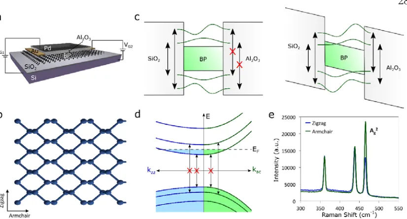
Figure 1.1: Static metasurfaces. a) A nano-antenna array plasmonic metasurface consisting of blocks of v-shaped gold nanostructures that exhibits negative refraction and b) A hyperbolic metasurface consisting of a thin metallic grating on a dielectric substrate designed to enhance the emission rate of quantum emitters. Reproduced from Reference 5.
If dynamic, tunable control of the near and far-field propagation of light can be achieved in
real time, a number of promising applications may be expected to emerge. Electrically
tunable metasurface optical phased arrays could enable beam steering for high-speed,
solid-state lidar detectors. Other technology directions for active metasurfaces include holographic
displays for virtual and augmented reality, LED lighting wi-fi (li-fi), and active thermal
radiation management. Beyond metamaterials, new devices and materials for high-speed
optical modulation could revolutionize telecommunications for both long and short-haul
interconnects in and around electronic microprocessors, or even to usher in entirely new,
all-optical computing paradigms.6, 7
While several paradigms have been posed for dynamically tunable optical materials,
electrical tuning promises uniquely compelling advantages in speed, reliability and cost.
Phase changes materials, for example, can generate large tunability in the refractive index,
but suffer from slow switching speeds, hysteresis, and low reliability. Likewise, thermal
effects can be utilized in CMOS materials, but are slow as well, and are typically difficult to
miniaturize due to problems with cross-talk. Semiconductor charge injection can occur at
gigahertz speeds, and field-based effects like the Stark shifting of semiconductor quantum
wells can be even faster. Thus, the research and development of ideal, electrically tunable
optical materials is critical to the viability of these technologies.
1.2Van der Waals Materials
Van der Waals materials are two-dimensional crystals that stack together in sheets, adhered
only by van der Waals interactions.8 The two-dimensional nature of these layers has a
number of important impacts on their electronic, optical, mechanical and thermal properties.
For example, the band structure of graphene, the most studied van der Waals material, is
radically different than that of graphite, its bulk form. The unique electronic landscapes in
these materials may be thought of as deriving from quantum confinement, and precipitate a
range of novel optoelectronic phenomena.9
The family of explored van der Waals materials is growing rapidly, and now includes
insulators, metals and semiconductors with light-matter interactions that span the
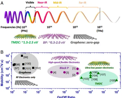
electromagnetic energy spectrum, as depicted in Figure 1.2. Most importantly for
electrically-tunable nanophotonics, the ultra-thin geometry of van der Waals materials
enables efficient modification of their optical properties via field-effect gating and other
Figure 1.2: The family of van der Waals materials spans a) light-matter interactions across the electromagnetic spectrum and b) a range of mobility and on / off ratio values. Reproduced from Reference 10.
The electro-optical responses of a small number of two-dimensional materials have already
been explored. In graphene, for example, a plasmonic response can be generated and
modulated at mid to far-infrared frequencies by adding electrons or holes via field-effect
gating.11 At near-infrared frequencies, gating allows Paul-blocking of interband optical
transitions, wherein filling or depleting the electronic states associated with these transitions
shuts them off or turns them on.12 In other two-dimensional materials, strongly bound
excitons generate strong light-matter interactions in the visible and near-infrared that can be
tunability can be achieved near a dominant visible frequency exciton peak by broadening
the spectral width of this peak via charge injection.
Black phosphorus is a new and compelling candidate for van der Waals optoelectronics. This
layered, semiconducting allotrope of phosphorus, evolves continuously from a bulk-like
semiconductor to a natural quantum well structure when thinned down to the few-layer limit.
As the layer count is reduced, quantum confinement increases the band gap from 0.3 eV in
bulk to approximately 2 eV for monolayers.10 In this regime, few layer black phosphorus
may be expected to exhibit tunable optoelectronic behavior along the lines of that seen in
compound semiconductor quantum well structures, which are ideal amplitude and phase
modulators. In addition, the anisotropic crystal structure of black phosphorus induces severe
anisotropy in its electronic, thermal, and optical properties.10 This anisotropy opens the door
for compelling new physics, such as hyperbolic plasmons, and technology applications, such
as polarization control and beam-steering of propagating surface waves.
As the family of van der Waals materials expands, we can hope to both shed light on novel
physics, and develop a new toolbox for dynamic nanophotonics and optoelectronics that will
enable new technology.
1.3Topological Materials
Topological materials, and specifically topological insulators, are a second class of
promising new materials for active nanophotonics. Three-dimensional electronic topological
insulators are band insulators with Dirac semimetallic surface states in which carrier spins
are locked in plane, orthogonal to their crystal momentum.13, 14 These surface states are
remarkably robust; they span the entire bulk band gap, and are topologically protected against
material defects and reconstructions that do not break time reversal symmetry.15 In addition,
back-scattering events – in which both momentum and spin directions must flip – are strongly
suppressed. Many of these compounds, such as the bismuth and antimony chalcogenides,
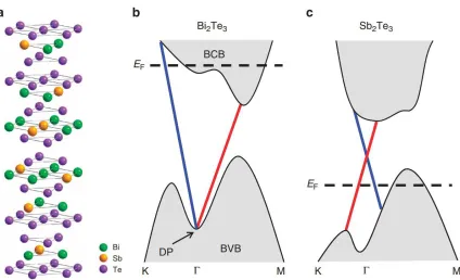
Figure 1.3: a) The van der Waals crystal structure of bismuth antimony telluride, and b), c) the electronic band structures of bismuth telluride and antimony telluride, respectively. The two spin-polarized surface state bands, which intersect at the Dirac point, are shown in blue and red. Reproduced from Reference 16.
Over the last decade, a range of new electronic phenomena have been observed in topological
insulator systems, including the quantum anomalous Hall effect.17 These materials have also
been predicted to host physically and technologically compelling optical and optoelectronic
behavior. Some of these effects have been experimentally demonstrated – giant
magneto-optical effects, helicity-dependent photocurrents and more – but many other remarkable and
novel light-matter interactions, including gapless infrared photodetection, gate-tunable,
long-lived Dirac plasmons, and hybrid spin-plasmon modes, remain to be seen and explored.18-22
Plasmonics is one promising direction for electrically tunable optoelectronics in topological
insulators. Due to the suppression of carrier back scattering, plasmon resonances are
expected to exhibit reduced dissipation and enhanced lifetimes. In addition, spin-momentum
locking is predicted to hybridize they typical charge degree of freedom with spin, yielding
can be tuned from purely charge-like excitations to purely spin-like excitations by changing
the carrier densities on the top and bottom surfaces via field-effect gating.
A second exciting direction is the electrical control of surface and bulk interband and
intraband optical transitions in topological insulators via field-effect gating. These four types
of optical transitions can in principle all be modulated, much like Paul-blocking and free
carrier effects in graphene. By controlling these interactions, topological insulators could
enable efficient optical modulation, tunable coupling to spintronic systems, or other
paradigms yet to be explored.
While topological insulator optoelectronics is an area ripe with opportunity, materials
challenges persist. To see these concepts to fruition, ideal materials must be developed that
exhibit strong light matter interactions with the topological surface states, and weak bulk
carrier interactions.
1.4The Scope of this Thesis
This thesis explores novel light-matter interactions in quantum materials, and how such
phenomena may be applied for active nanophotonics.
Chapters 2 and 3 of this thesis focus on new optoelectronic phenomena in few-layer black
phosphorus. In Chapter 2, we demonstrate the Pauli-blocking of intersubband optical
transitions in black phosphorus quantum wells under carrier injection. In Chapter 3, we
demonstrate the quantum-confined Stark effect in black phosphorus, and examine the role of
anisotropy in black phosphorus optics. We further explore how anisotropic
electro-optical effects in few-layer black phosphorus yield tunable birefringence and dichroism.
Chapter 4 of this thesis focuses on optical transitions in bismuth antimony telluride
topological insulator materials. We demonstrate electrical control of bulk interband
transitions, and both topological surface and bulk intraband transitions. We construct a
surface interband transitions, and develop a method for epitaxial lift-off of bismuth
antimony telluride films from common epitaxy substrates.
Chapter 5 of this thesis reports theory results indicating that resonant nanophotonic devices
loaded with few-layer black phosphorus can act as ideal, polarization-dependent phase and
amplitude modulators with highly efficient performance. This chapter serves as an example
application of the fundamental research described in Chapters 2 through 4, and highlights an
important direction for future work.
Chapter 6 of this thesis reports existing results and immediate plans for ongoing work, and
provides a perspective on future directions. First, we describe initial results from an ongoing
effort to observe gate-tunable, anisotropic plasmon resonances in black phosphorus
nanoribbon structures. Next, we propose a program of experiments to follow up on the
theory results from Chapter 5. We further propose a direction for future experiments on
hybrid spin-plasmon modes in topological insulator materials. Lastly, we provide a
perspective on both the work described herein, and the scientific and technological impact
we might expect from future research on electrically tunable light matter interactions in
quantum materials.
Chapter 2
Charge-Driven Modulation of Intersubband
Optical Transitions in Few-Layer Black
Here, we report measurements of the infrared optical response of thin black phosphorus
under field-effect modulation.23 We interpret the observed spectral changes as a combination
of an ambipolar Burstein-Moss (BM) shift of the absorption edge due to band-filling under
gate control, and a quantum confined Franz-Keldysh (QCFK) effect, phenomena which have
been proposed theoretically to occur for black phosphorus under an applied electric field.
Distinct optical responses are observed depending on the flake thickness and starting carrier
concentration. Transmission extinction modulation amplitudes of more than two percent are
observed, suggesting the potential for use of black phosphorus as an active material in
mid-infrared optoelectronic modulator applications.
2.1Introduction
The emergence of a variety of two-dimensional materials has spurred tremendous research
activity in the field of optoelectronics24-27. While gapless graphene can in principle exhibit
an optoelectronic response at wavelengths ranging from the far infrared to the ultraviolet, its
optoelectronic behavior is limited by a lack of resonant absorption and poor optical
modulation in the absence of one-dimensional confinement. On the other hand, the
semiconducting molybdenum- and tungsten-based transition metal dichalcogenides have
shown considerable prospects for visible frequency optoelectronics. Yet while these
materials promise exciting new directions for optoelectronics and nanophotonics in the
visible range, they have limited response for lower energy, infrared light.
The isolation of atomically thin black phosphorus in recent years has bridged the wavelength
gap between graphene and transition metal dichalcogenides, as black phosphorus is an
emerging two-dimensional semiconductor material with an infrared energy gap and typical
carrier mobilities between those of graphene and transition metal dichalcogenides.28-32 Since
the first isolation of black phosphorus and demonstration of a field effect device, numerous
reports investigating the synthesis and optoelectronic properties of this material have
emerged, appropriately summarized in recent reviews.10, 28, 29, 33, 34 Likewise a number of
reports have also appeared on the applications of black phosphorus in fast photodetectors35,
photodetectors38, visible to near-infrared absorbers39 and emitters, 40-43heterojunction30
and split gate p-n homojunction photovoltaics44, gate-tunable van der Waals heterojunctions
for digital logic circuits45, 46 and gigahertz frequency transistors in analog electronics47. A
majority of the studies on both the fundamental optical properties of black phosphorus and
applications in optoelectronic devices have explored only the visible frequency range48-51.
Therefore, little is known about the intrinsic optical response of black phosphorus in the
infrared range. As a narrow band-gap semiconductor, much of the potential for black
phosphorus lies in these infrared optoelectronic applications – ranging from tunable infrared
emitters52 and absorbers for waste heat management/recovery53 to thermophotovoltaics54 and
optical modulators for telecommunications55. Theoretical investigations of black phosphorus
have suggested novel infrared optical phenomena, such as anisotropic plasmons56, 57,
field-effect tunable exciton stark shifts58, and strong Burstein-Moss59 and quantum-confined
Franz-Keldysh effects60 that promise to open new directions for both fundamental
nanophotonics research and applications. In this work, we report the first experimental
observations of the infrared optical response of ultrathin BP samples under field effect
modulation. We observe modulation of oscillations in the transmission spectra which we
attribute to a combination of an ambipolar Burstein-Moss shift / Pauli-blocking effect and
quantum-confined Franz-Keldysh behavior.
2.2Experimental Measurements of the Black Phosphorus Optical Response with Doping by an Electrostatic Gate
Measurements were performed on black phosphorous flakes that were mechanically
exfoliated in a glove box onto a 285 nm SiO2/Si substrate. We analyzed three flakes of 6.5
nm, 7 nm, and 14 nm thickness, determined by Atomic Force Microscopy (details are
provided in the Supporting Information Fig. S6), and lateral dimensions of approximately 10
μm x 10 μm. A schematic of our experimental setup is shown in Figure 1a. Standard electron beam lithography and metal deposition methods were used to define Ni/Au electrodes to each
exfoliated BP flake. The samples were then immediately coated in 90nm PMMA for
protection against environmental degradation. Once encapsulated in PMMA we observe
spectroscopy61 and reported in literature precedent62. Transmission measurements were
obtained via Fourier Transform Infrared (FTIR) Spectroscopy. All optical measurements
were done in a Linkam cryo-stage at a pressure of 3 mTorr and a temperature of 80 K. First,
a room-temperature gate-dependent source-drain current was measured to extract
approximate carrier densities as a function of gate bias. Transmission spectra were then
gathered at different gate voltages applied between the flake and lightly doped Si substrate.
We note that in our setup, the silicon substrate is grounded and BP experiences the applied
voltage, so the sign of the applied voltages is reversed from the more common convention.
In order to probe the electric field- and charge-carrier-dependent optical properties of the BP,
all spectra were normalized to the zero-bias spectrum. The measured infrared optical
properties result primarily from the unique band structure of thin BP, schematically depicted
in Figure 1b. Quantized inter sub-band transitions provide the primary contribution to its
zero-field optical conductivity.
Figure 2.1: a) Schematic illustration of transmission modulation experiment. Broadband mid-IR beam is transmitted through black phosphorus sample. Variable gate voltage applied across SiO2 modulates transmission extinction, b) Schematic band diagram of few-layer black phosphorus with subbands arising from vertical confinement.
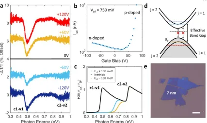
[image:24.612.109.536.369.584.2]We first present results for the 7 nm thick BP flake, in Figure 2. An optical image is shown
in Figure 2e. FTIR spectra were taken using a Thermo Electron iS50 FTIR spectrometer and
Continuum microscope for which the light source is a broadband, unpolarized tungsten
glo-bar. To improve signal/noise and minimize spatial drift, we surrounded the sample with a
150 nm thick gold reflector which also served as the gate electrode. The extinction
modulation results are presented in Figure 2a. We observe two major features in this flake at
energies of 0.5 eV (I) and 0.9 eV (II). The dip in extinction at 0.5 eV is present for both
positive and negative gate voltages, as the sample is increasingly hole or electron doped,
respectively. It grows in strength as the doping is further increased at larger gate-biases. The
same trend is true for the feature at 0.9 eV, where a smaller peak in extinction modulation is
observed for both polarities of voltage. This peak also is strengthened as the gate voltage is
increased to +/- 120V. To gain insights into this behavior, we measure gate-dependent
transport, using a scheme in which a positive bias induces hole-doping, and a negative bias
introduces electron-doping. We observe ambipolar transport at room temperature and
atmospheric conditions, as shown in Figure 2b. Similar results have been shown in the
literature with on/off ratios of ~104 for flakes thinner than the one considered here, at low
temperature.30, 63 From this, the CNP is observed to be at 20 V, and, using the parallel plate
model described in the Supporting Information, the unbiased, n-type carrier concentration is
Figure 2.2: Gate modulation of lightly doped 7 nm flake. a) FTIR transmission extinction vs photon energy normalized to zero bias b) Source-drain current vs gate voltage. Ambipolar conduction is seen. c) Calculated optical conductivity of a 4.5 nm thick BP flake at different carrier concentrations, normalized to the universal conductivity of graphene. No field effects included. d) Schematic of electronic band structure and allowed interband transitions at different voltages. e) Optical microscope image of flake. Scale bar is 10μm.
We can interpret our spectroscopic results with consideration of a Burstein-Moss shift, which
is a well-known phenomenon in chemically doped narrow-band gap semiconductor
materials. This effect, which changes the optical band gap of a semiconductor, results from
band-filling or Pauli-blocking. As the charge carrier density is increased and the Fermi level
moves into the conduction or valence band, there are fewer unoccupied electronic states
available, and optical transitions to the occupied states are disallowed. This results in a
decrease in the optical conductivity of the material at the energy of the transition, and is
manifest in measurements as a decrease in absorption.64, 65 Because this flake exhibits
ambipolar transport behavior, we can explain both features (I) and (II) as arising from an
ambipolar BM effect. At zero applied bias, the flake is very lightly doped, and all optical
transitions are allowed. As a positive gate voltage is applied and the sample becomes hole
decreases. Feature (I) corresponds to the Pauli-blocking of the E11 intersubband transition,
and feature (II) corresponds to the blocking of the E22 intersubband transition, shown
schematically in Figure 2d. For a negative gate voltage, as the sample is electron-doped and
the Fermi level moves into the conduction band, the E11 and E22 transitions are again blocked
due to band filling, resulting again in a decrease in absorption. To support this explanation,
we calculate the optical conductivity for the flake, as shown in Figure 2c to identify the
appropriate energies of the intersubband transitions. To do so, we use the Kubo method
described by Tony Low, et al.59, to calculate the components σαβ of the optical conductivity tensor. Further details on the Hamiltonian, eigenfunctions and eigenvalues, velocity operator
and more are available in that reference, and Matlab code used to perform the calculation is
available in the Appendix.
𝜎𝜎𝛼𝛼𝛼𝛼(𝒒𝒒,𝜔𝜔) =−𝑖𝑖𝑔𝑔𝑠𝑠ℏ𝑒𝑒 2
(2𝜋𝜋)2 � � 𝑑𝑑𝒌𝒌
𝑓𝑓�𝐸𝐸𝑠𝑠𝑠𝑠𝒌𝒌� − 𝑓𝑓�𝐸𝐸𝑠𝑠′𝑠𝑠′𝒌𝒌′� 𝐸𝐸𝑠𝑠𝑠𝑠𝒌𝒌− 𝐸𝐸𝑠𝑠′𝑠𝑠′𝒌𝒌′ 𝑠𝑠𝑠𝑠′𝑠𝑠𝑠𝑠′
×�Φ𝑠𝑠𝑠𝑠𝒌𝒌𝐸𝐸�𝑣𝑣�𝛼𝛼�Φ𝑠𝑠′𝑠𝑠′𝒌𝒌′��Φ𝑠𝑠′𝑠𝑠′𝒌𝒌′�𝑣𝑣�𝛼𝛼�Φ𝑠𝑠𝑠𝑠𝒌𝒌�
𝑠𝑠𝑠𝑠𝒌𝒌− 𝐸𝐸𝑠𝑠′𝑠𝑠′𝒌𝒌′ +ℏ𝜔𝜔+𝑖𝑖𝑖𝑖 (2.1)
We note that this optical conductivity is normalized to 𝜎𝜎0 = 𝑒𝑒2⁄4ℏ, the universal optical conductivity of graphene. It can then be used to calculate the (non-normalized) dielectric
function, using the static dielectric constant 𝜖𝜖𝑟𝑟𝑟𝑟𝑟𝑟 and black phosphorus thickness Δ.
𝜖𝜖𝑠𝑠𝑠𝑠(𝜔𝜔) =𝜖𝜖𝑟𝑟𝑟𝑟𝑟𝑟+𝑖𝑖𝑒𝑒 2 4ℏ
𝜎𝜎𝑠𝑠𝑠𝑠(𝜔𝜔)
Δ𝜖𝜖0𝜔𝜔 (2.2)
The observed transitions energies are consistent with theoretical models that predict an
increase in band gap energy from the bulk 0.3 eV value as the material thickness decreases
to several layers or less.50 This deviation from the bulk band gap indicates the influence of
vertical confinement of charge carriers, a feature of the two-dimensionality of the material.
We note that these transition energies suggest that the true thickness of our sample is thinner
than 7 nm, at approximately 4.5 nm. This apparent variation between true and observed
reported.66 The surface oxide on our samples is expected to be between 1-2 nm on either
side, which appears inevitable despite following best practices, and is stable with no
measurable degradation over an ambient exposure of > 18 hrs in ambient (see Supporting
Information). It is noteworthy that we observe extinction modulation at relatively high
photon energies, indicative of very large charge modulation taking place in the fraction of
the BP nearest to the silicon oxide interface, with an accumulation/depletion layer that decays
over the remainder of the flake. This is consistent with in-depth calculations of charge
screening in BP using the Thomas-Fermi model done previously, reported by Tony Low, et
al.56 We estimate this screening length to be of order 3 nm for our devices in the Supporting
Information. This ambipolar, gate-modulated Burstein-Moss shift is the first observed in a
two-dimensional semiconductor, to the best of our knowledge.
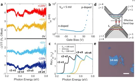
2.2.2 14 nm Flake with Light Doping
We next present data for a BP flake of 14 nm thickness in Figure 3. An optical image is
shown in Figure 3e. Extinction measurements are again taken with an iS50 FTIR
spectrometer and Continuum microscope for which the light source is a tungsten glowbar.
These results are presented in Figure 3a. Four prominent features are observed to modulate
under application of a gate voltage, at energies of 0.35 eV, 0.41 eV, 0.55 eV, and 0.75 eV.
As in the previous sample, they grow in strength with increased magnitude of the gate
voltage, regardless of polarity. To better understand this behavior, we again measure
gate-dependent transport, reported in Figure 4b. We observe ambipolar transport characteristics
as in the previous flake, centered about a conductance minimum at approximately 20 V.
Again using a parallel-plate capacitor model, we estimate an unbiased n-type carrier density
Figure 2.3: Gate modulation of lightly doped 14 nm flake. a) FTIR transmission extinction vs photon energy normalized to zero bias b) Source-drain current vs gate voltage. Ambipolar conduction is seen. c) Calculated optical conductivity of a 10 nm thick BP flake at different carrier concentrations, normalized to the universal conductivity of graphene. No field effects included. d) Schematic of electronic band structure and allowed interband transitions at different voltages. e) Optical microscope image of flake. Scale bar is 10 µm.
We propose that the optical modulation for this sample also results from an ambipolar
Burstein-Moss effect. In this case, as the Fermi energy is moved into the conduction band
of the BP under negative bias, transitions become disallowed and the transmission is
increased at each of the E11 – E44 energies. Under positive bias, as the Fermi energy is moved
into the valence band, the band-filling effect of opposite charge carrier type results in
negative extinction modulation peaks at the same energies of transitions E11 – E44. As in the
previous sample, we estimate an oxide layer of 1-2 nm has grown on our BP on either surface.
Based on optical conductivity calculations presented in Figure 3c, we again estimate the
adjusted thickness of our flake to be less than that measured by AFM, at approximately 10
nm. We further note that for this sample, the measurement extended beyond the area of the
We thus suggest that the true modulation strength of this device is of order six percent, not
the 0.75 percent indicated by the modulation of the entire area.
2.2.3 6.5 nm Flake with Heavy Doping
Finally, results for the 6.5 nm thick flake are reported in Figure 4, for which an optical image
is shown in Figure 4e. Unlike the previous two flakes, transmission measurements for this
sample were taken using a Nicolet Magna 760 FTIR spectrometer coupled to a Nic-Plan
infrared microscope on infrared Beamline 1.4.3 at the Advanced Light Source (ALS) at
Lawrence Berkeley National Laboratory. This allowed us to perform measurements using a
high brightness, diffraction-limited infrared beam, which is beneficial for accurately
analyzing the small-area BP samples attainable by mechanical exfoliation. In contrast to the
previous measurements, the incident light was elliptically polarized due to the synchrotron
source, with an intensity ratio of two to one. The major axis and details of the polarization
state are indicated and discussed in Supporting Information Figure S3.
[image:30.612.111.538.397.646.2]allowed interband transitions at different voltages. d) Schematic representation of quantum confined Franz-Keldysh Effect e) Calculated optical conductivity of a 6.5 nm thick BP flake at different carrier concentrations, normalized to the universal conductivity of graphene. No field effects included f) Optical microscope image of flake. Scale bar is 10 μp.
Figure 4a shows the primary result of this experiment, which is the modulated extinction of
the sample at different voltages, normalized to the zero-bias extinction spectrum. Three
prominent features are observed in these spectra. First, under negative applied bias (i.e.: when
the sample is being depleted of holes), a negative peak (I) appears in transmission near 0.45
eV, which grows in amplitude and broadens to lower energies as the magnitude of the bias
increases. Second, under positive applied bias (i.e.: when the sample is being increasingly
hole-doped), a positive peak (II) appears in transmittance near 0.5-0.7 eV. Lastly, these two
effects, which we propose to depend on the Fermi level, are superimposed with an oscillatory
feature (III) that varies with the magnitude of the applied field, but not its polarity, and which
is most clearly visible in the negative bias spectra in the 0.5 - 0.7 eV range.
To better understand these results, transport measurements were again taken at room
temperature under ambient conditions, as shown in Figure 4b. The gate dependence of the
conductance indicates that, unlike the previous samples, this BP flake was initially heavily
hole-doped, as ambipolar transport is not observed and only hole-type conduction is seen
even at large negative bias. This indicates a zero-bias carrier concentration in excess of 6∙1012 cm-2.
Due to the distinct character of each feature and their relation to the transport measurements,
we can understand the overall spectral shifts as arising from a combination of a
Burstein-Moss (BM) shift and a quantum confined Franz-Keldysh (QCFK) effect, both of which have
been predicted theoretically for gated BP flakes of this thickness.60 In the bulk limit, the
Franz-Keldysh effect refers to electron and hole wavefunctions leaking into the band gap, as
described by Airy functions. This behavior introduces oscillatory features to the interband
absorption spectrum, and redshifts the band edge. In confined systems, the
confinement becomes stronger and excitonic effects dominate, this phenomenon
eventually gives way to the quantum-confined Stark effect. Because our flake exceeds a
thickness of ~4 nm, we expect excitonic effects to be weak and therefore will not focus our
discussion on the quantum-confined Stark effect or a normal-to-topological phase transition
in our analysis.50, 51, 58
We suggest that peak (I) at 0.45 eV can be described by the onset of j = 1 intersubband
transitions as the material is depleted of holes at negative gate voltages and the valence band
is un-filled, in agreement with our transport measurements. We further suggest that peak (II)
can be described primarily by the suppression of j = 2 inter sub-band transitions as more
holes are accumulated in the flake at positive gate voltages. This behavior is shown
schematically in Figure 4d, and is again supported by calculations of the optical conductivity
of the flake for various doping levels, shown in Figure 4e. Our experimental results
correspond to modulation of the calculated intersubband transitions only in part, suggesting
that a simple Burstein-Moss shift is insufficient to explain this measurement. From these
results, we assign the band gap energy of our flake to be approximately 0.4 eV. Unlike our
previous samples, the optical data indicates minimal oxide formation, as the E11 and E22
transition energies match well to theory for a 6.5 nm thick BP quantum well. Given we do
not see the charge neutral point in transport, we do not assign a carrier density to this flake,
but can say that with a charge neutral point of greater than -80 V, its p-type carrier density
must be greater than 6∙1012 cm-2.
We suggest that quantum-confined Franz-Keldysh effects lead to the appearance of the
additional oscillatory spectral features we observe. Specifically, we point to the oscillations
in the negative voltage extinction curves at energies above 0.5 eV – where Burstein-Moss
considerations would predict zero modulation – and in the positive voltage extinction curves
both in that same range – where Burstein-Moss behavior would predict only a single dip in
extinction centered at the 0.575 transition energy – and at 0.45 eV. This oscillatory
modulation increases with bias magnitude, but does not depend significantly on the sign of
conduction and valence sub-band wavefunctions, as described by the quantum-confined
Franz-Keldysh effect. This behavior is investigated theoretically for gated BP by Charles
Lin, et al.60 In addition, under a sufficiently strong electric field, hybrid optical transitions
between sub-bands of different index (eg: Ev1 to Ec2) that are nominally forbidden at zero
field become allowed. In total, quantum-confined Franz-Keldysh effects in thin BP are
expected to lead to behavior including redshifting of intersubband transitions, modification
of intersubband selection rules (allowing hybrid transitions), or oscillatory, Airy function
modulation of the absorption edge, all of which can be considered as consistent with our
experimental observations. However, further theoretical work is needed to understand this
effect satisfactorily; the same authors provide evidence in a more recent, experimental report
that hybrid transitions may occur with zero applied field as well.68 Interestingly, we see no
evidence of a tunable plasma edge; investigations in the long-wave infrared wavelength
range with larger samples would likely be needed to observe this feature.
The clear appearance of the QCFK effect in this measurement distinctly differs from our
previous two samples, indicating that BP quantum wells of similar thickness may have very
different optical responses. We suggest that the primary reason for this is that this flake is
very heavily doped under zero bias, whereas our previous measurements were performed on
nearly intrinsic flakes. In particular, in the intrinsic case, field strength and carrier
concentration vary proportionally (ie: under larger bias, there is a larger carrier concentration,
and vice-versa). To the contrary, in our heavily doped sample, this proportionality is absent,
leading to potentially competing effects and the clear emergence of oscillatory features. It is
also worth noting that, while we see no clear evidence of the QCFK effect in our first two
experiments, it is possible that the large BM shift is simply dominant over the QCFK effect,
making the latter effect difficult to observe, or that our increased noise prevents the effect
from obviously manifesting. A complete theoretical framework that addresses the interplay
between zero-bias carrier concentration and field-effect has not yet been developed, and is
beyond the scope of this paper. We also note that, while we see no clear evidence of excitonic
not be present in flakes of this thickness, we do not rule out the possibility that they may
be influencing our results.
We note that because of the complicated polarization state of incident light from the
synchrotron, and because a previous study has extensively studied this effect
experimentally69, we do not address in detail the anisotropic optical properties of BP.
However, due to the primary contribution to the optical conductivity arising from the σxx component, we argue that the only effect of elliptically polarized light is to scale the observed
modulation, as discussed in the Supplement Section 1 - 3.
2.3 Conclusion
In conclusion, we have demonstrated experimentally that ultra-thin black phosphorus
exhibits widely tunable, quantum well-like optical properties at mid-infrared wavelengths.
In 7 and 14 nm, lightly doped flakes, we observe for the first time an ambipolar
Burstein-Moss shift of intersubband transitions, which also varies with thickness as these transition
energies are changed. In a heavily doped 6.5 nm thick BP flake, modulation of infrared
transmission takes place as a result of both a Burstein-Moss shift and additional,
quantum-confined Franz-Keldysh effects. While our results verify some of the recent theoretical
predictions about the electro-optical effects in few-layer BP, they also report new behavior
and serve as motivation to further understand the BP optical response as function of sample
thickness, doping and field. Our results indicate that BP is both an interesting system for
exploring the fundamental behavior of quantum-confined carriers in two-dimensional
semiconductors under field-effect modulation, and a promising candidate for tunable
Chapter 3
In this work, we report the first known examples of electrically tunable bifringence and
linear dichroism, observed here in few-layer black phosphorus (BP).70 We observe these
effects across mid-infrared and visible frequencies, suggesting that BP is an ideal
material system for actively controlling the complex polarization state of light – or even
the propagation direction of surface waves. This phenomenon is driven by anisotropic
Burstein-Moss (Pauli-blocking) and quantum-confined Stark effects, which we
distinguish via different gating schemes, as well as by modification of quantum well
selection rules under applied field. We further observe that these effects generate
near-unity tuning of BP absorption for certain material thicknesses and photon energies.
3.1Introduction
As photonic structures for controlling the near- and far-field propagation of light become
increasingly complex and compact, the need for new materials that can exhibit unique,
strong light-matter interactions in the ultra-thin limit is growing rapidly. Ultrathin van der
Waals materials are especially promising for such applications, as they allow for the
control of light at the atomic scale, and have properties that can be modulated actively
using an external gate voltage.71, 72 Of these, few-layer black phosphorus (BP) is
particularly noteworthy due to its high electronic mobility, and a direct band gap that can
be tuned as a function of thickness from 0.3 eV to 2 eV.29, 73 This has enabled the
realization of numerous optoelectronic devices with high performance, including
photodetectors that can be easily integrated with other photonic elements such as
waveguides.37, 74-77 In addition to this static control, recent works using electrostatic
gating and potassium ions have shown that the electronic band gap of BP may be tuned
by an electric field.51, 78-80
One of the most salient features of BP is its large in-plane structural anisotropy, leading
to a polarization-dependent optical response49, 57, 81 as well as mechanical82, thermal83,
and electrical transport characteristics36, 84 that vary with in-plane crystallographic
orientation.31 This optical anisotropy corresponds to a large, broadband birefringence85,
between polarization states of light. Moreover, mirror-symmetry in the x-z plane
forbids intersubband optical transitions along the zigzag axis, and as a result, BP exhibits
significant linear dichroism, wherein the material absorption depends strongly on the
polarization state of exciting light.81, 86
In this work, we experimentally demonstrate that the application of a static electric field
enables the tunability of the linear dichroism of few-layer black phosphorus (BP). This
response – which approaches near-unity tunability of the BP oscillator strength for some
thicknesses and photon energies – is achieved by active control of quantum-confined
Stark and Burstein-Moss effects, and of quantum-well selection rules. We observe
anisotropic tunability from the visible to mid-infrared (mid-IR) spectral regimes,
behavior not seen in traditional electro-optic materials such as graphene87, transparent
conducting oxides88, 89, silicon90, and quantum wells.91 This opens up the possibility of
realizing novel photonic structures in which linear dichroism in the van der Waals plane
can be continuously tuned with low power consumption, because the switching is
electrostatic in nature. By controlling optical losses in the propagation plane, for
example, efficient in-plane beam steering of surface plasmon polaritons or other guided
modes is enabled. Moreover, an electrically tunable polarizer could be realized by
modulating the polarization state of light absorbed in a resonant structure containing BP.
Because this tunability is strongest at infrared wavelengths, it could also enable control of
the polarization state of thermal radiation.52, 92, 93
3.2Experimental Measurements of the Black Phosphorus Optical Response with an Applied Electric Field
In order to probe and distinguish the electro-optical tuning mechanisms evident in
few-layer BP, we used a combination of gating schemes wherein the BP either floats in an
applied field or is contacted, as shown in Fig. 1a and described further in the Methods
section. Polarization-dependent optical measurements are taken aligned to the crystal
axes, in order to probe the structural anisotropy shown in Fig. 1b. This enables us to
external field-effects – i.e.: the quantum-confined Stark effect and control of forbidden
transitions in the infrared – to the tunability of linear dichroism, qualitatively illustrated
in Figures 1c and 1d.23, 59, 60, 79 In the anisotropic Burstein-Moss (BM) shift, the optical
band gap of the material is changed as a result of band filling and the consequent
Pauli-blocking of intersubband transitions. As the carrier concentration of the sample is
changed, the Fermi level moves into (out of) the conduction or valence band, resulting in
a decrease (increase) of absorptivity due to the disallowing (allowing) of optical
transitions.64, 94 Because intersubband optical transitions are only allowed along the
armchair axis of BP, this tunability occurs only for light polarized along this axis. In the
quantum-confined Stark Effect, the presence of a strong electric field results in the
leaking of electron and hole wave functions into the band gap as Airy functions,
red-shifting the intersubband transitions energies.95 In quantum well structures, this
red-shifting is manifested for multiple subbands, and therefore can be observed over a wide
range of energies above the band gap. To assess the gate-tunable anisotropy of the optical
response of BP, the armchair and zigzag axes, illustrated in Fig. 1b, of the samples
considered are identified by a combination of cross-polarized visible microscopy,
described in the Supporting Information S1, and either polarization-dependent Raman
spectroscopy or infrared measurements, described below. Representative Raman spectra
are presented for the visible frequency sample on SrTiO3 in Figure 1e. The optically
active armchair axis exhibits a maximum intensity of the Ag2 resonant shift at 465 cm-1,
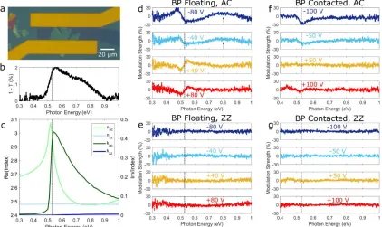
Figure 3.1. Anisotropic electro-optical effects in few-layer BP. (a) Schematic figure of infrared tunability devices. Few-layer BP is mechanically exfoliated on 285 nm SiO2/Si and then capped with 45 nm Al2O3 by ALD. A semitransparent top contact of 5 nm Pd is used to apply field (VG1) while the device floats and 20 nm Ni/200 nm Au contacts are used to gate (VG2) the contacted device. (b) Crystal structure of BP with armchair and zigzag axes indicated. (c) Illustration of quantum-confined Stark effect and symmetry-breaking effect of external field. Under zero external field, only optical transitions of equal quantum number are allowed. An external field tilts the quantum well-like energy levels, causing a red-shifting of the optical band gap and allowing previously forbidden transitions. (d) Illustration of anisotropic Burstein-Moss shift in BP. Intersubband transitions are blocked due to the filling of the conduction band. Along the ZZ axis, all optical transitions are disallowed regardless of carrier concentration. (e) Raman spectra with excitation laser polarized along AC and ZZ axes. The strength of the Ag2 peak is used to identify crystal axes.
3.2.1 3.5 nm Flake
To illustrate the mechanisms of tunable dichroism of BP in the mid-infrared, we measure
tunability of transmittance using Fourier-Transform Infrared (FTIR) microscopy as a
function of externally (VG1) or directly applied bias (VG2), presented for a 3.5 nm thick
flake, as determined from atomic force microscopy (AFM) (Figure S1, Supporting
Information), in Figure 2. Fig. 2b presents the raw extinction of the flake along the
armchair axis at zero bias, obtained by normalizing the armchair axis extinction to that of
[image:39.612.125.538.78.300.2]consistent with a thickness of 3.5nm. A broad, weak shoulder feature is observed at
approximately 0.75 eV. The corresponding calculated optical constants for the flake (see
[image:40.612.113.535.176.427.2]Methods for calculation details) are presented in Figure 2c for comparison.
Figure 3.2. Electrically tunable linear dichroism: quantum-confined Stark and Burstein-Moss effects and forbidden transitions. (a) Optical image of fabricated sample; (b) Zero-bias infrared extinction of 3.5 nm flake, polarized along armchair (AC) axis. (c) Calculated index of refraction for 3.5 nm thick BP with a Fermi energy at mid-gap. (d) Tunability of BP oscillator strength with field applied to floating device, for light polarized along the AC axis. (e) Corresponding tunability for light polarized along the zigzag (ZZ) axis. (f) Tunability of BP oscillator strength with gating of contacted device, for light polarized along the AC axis. (g) Corresponding tunability for light polarized along the ZZ axis.
Figures 2d and 2e illustrate the influence of an external field on the extinction of BP with
carrier concentration held constant (i.e. the BP is left floating). The extinction data for
each voltage is normalized to the zero bias case and to the peak BP extinction seen in
Figure 2b, to obtain a tuning strength percentage that quantifies the observed tunability of
the BP oscillator strength. We note that this normalization scheme underestimates the
armchair axis, presented in Fig. 2d, two tunable features are measured near photon
energies of 0.5 and 0.8 eV. We explain the first feature at 0.5 eV as arising from a
shifting of the BP band edge due to the quantum-confined Stark effect. At negative bias,
the band gap effectively shrinks and this is manifest as a redistribution of oscillator
strength near the band edge to lower energies. As a result, an increase in absorptance is
measured below the zero-bias optical band gap, and a decrease is seen above it. At
positive bias, this trend is weakened and reversed. We propose two explanations for this
asymmetry: the first is the influence of electrical hysteresis, and the second is the
presence of a small internal field in the BP at zero bias, which has been observed in
previous works on the infrared optical response of few-layer BP.81
The second, higher energy feature observed in the measured spectrum does not
correspond to any predicted intersubband transition. Rather, we propose it arises due to
the allowing of an optical transition that was previously forbidden by quantum-well
selection rule constraints dictated by symmetry (i.e. only transitions of equal quantum
number are allowed under zero field59). We note that this feature is present in the 0 V
extinction spectrum, consistent with a zero-bias internal field. As the symmetry is further
broken with an externally-applied electric field, this transition is strengthened. Under
positive bias, the internal and external fields are in competition, resulting in minimal
change. This suppressed tunability can also be attributed to hysteresis, as before.
In Figure 2e, no tunability is measured for any applied bias for light polarized along the
zigzag axis. This can be well understood due to the dependence of the Stark effect on the
initial oscillator strength of an optical transition; because no intersubband optical
transitions are allowed along this axis, the field effect is weak. Similar behavior has been
observed in excitons in ReS2 based on an optical Stark effect.97 Moreover, while the
externally applied field can allow ‘forbidden’ transitions along the armchair axis by
breaking the out-of-plane symmetry of the quantum well, in-plane symmetry properties
unaffected. This selection rule and the corresponding symmetry properties have been
previously described.36
In Figures 2f and 2g, we present the complementary data set of tunable dichroism
measurements due to a directly applied gate bias with electrical contact made to the BP in
a standard field-effect transistor (FET) geometry. Here, we observe tunability dominated
by carrier concentration effects. At the band gap energy of approximately 0.53 eV, a
simple decrease in absorptance is observed at negative and large positive biases,
consistent with an ambipolar BM shift. Unlike the results of applying field while the BP
floats, no tunability of the forbidden transition at 0.75 eV is observed; this is explained in
part due to the screening of the electric field due to the carrier concentration tunability.
We additionally may consider the possibility that this optical transition is disallowed by
Pauli-blocking effects, negating the symmetry-breaking effect of the directly applied
field. As in the case for the floating BP measurement, no tunability is observed along the
zigzag axis.
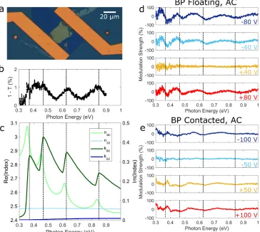
3.2.2 8.5 nm Flake
The anisotropic electro-optical effects described above change character rapidly as the
BP thickness – and hence band gap and band structure – is varied. Figure 3 presents
analogous results on a flake of 8.5 nm thickness, determined by AFM (see Supporting
Information, Fig. S1), for which an optical image is presented in Fig. 3a. Due to the
increased thickness, the energy separation between subbands is smaller, resulting in a
narrower free-spectral range between absorptance features measured in the zero-bias
spectrum, presented in Fig. 3b and for which corresponding calculated optical constants
are presented in Fig. 3c. Results for tunability by an external field with the BP left
floating are presented in Fig. 3d. As in the thin flake, substantial tuning of the
absorptance at each intersubband transition is observed due to the quantum-confined
Stark effect (QCSE) red-shifting the energy of the subbands. Due to the large Stark
coefficient in BP – which increases with thickness in the few-layer limit – absorption is
the material.78, 98 Unlike the previous sample, tuning of forbidden transitions is not
apparent; all features correspond to transitions measured in the 0 V normalization scheme
as well as the calculated optical constants for a thickness of 8.5 nm. As before, no tuning
is seen along the zigzag axis, as shown in Figure S2, Supporting Information. In Fig. 3e,
the tunability for directly gated, contacted BP is shown. The observed tuning – a
reduction in extinction centered at each of the calculated intersubband transition energies
– is relatively weak and does not persist to high photon energies. This suggests that the
dominant tunability mechanism is the ambipolar BM shift, rather than the QCSE.
Additional measurements at lower energies are presented in Figure S3, Supporting
[image:43.612.142.506.308.634.2]Information.
BP oscillator strength with gating of contacted device, for light polarized along the AC axis.
3.2.3 Visible Frequency Modulation
In Figure 4 we present results of gate-tunable dichroism at visible frequencies in a 20 nm
thick flake, comparable to those considered for infrared tunability. A new device
geometry is used to enable transmission of visible light, shown schematically in Fig. 4a
and in an optical image in Fig. 4b. In this configuration, a SrTiO3 substrate is utilized to
allow transmission-mode measurements at visible wavelengths. A symmetric gating
scheme is devised based on semi-transparent top and back gate electrodes of 5 nm Ni, as
described in the Methods section. Only an applied field, floating BP measurement is
utilized, as band-filling effects should be negligible at this energy range. In Fig. 4c, we
present tunability results from 1.3 to 2 eV. Due to the QCSE, tunability is observed up to
1.8 eV, corresponding to red light. Thus we demonstrate that electro-optic tuning of
linear dichroism is possible across an extraordinarily wide range of wavelengths in a
single material system, enabling multifunctional photonic devices with broadband