Rochester Institute of Technology
RIT Scholar Works
Theses
Thesis/Dissertation Collections
11-1-1991
Development of a modular 2-micron BiCMOS
process from an existing 2-micron n-well CMOS
process
R. Michael Guidash
Follow this and additional works at:
http://scholarworks.rit.edu/theses
This Thesis is brought to you for free and open access by the Thesis/Dissertation Collections at RIT Scholar Works. It has been accepted for inclusion in Theses by an authorized administrator of RIT Scholar Works. For more information, please [email protected].
Recommended Citation
Approved
by:
DEVELOPMENT OF A
MODULAR 2-MICRON BICMOS PROCESS
FROMAN
EXISTING 2-MICRON N-WELL CMOS PROCESS
by
R. Michael Guidash
A Thesis Submitted
i
n
Partial
Fulfillment
of the
Requirements
for the Degree of
MASTER OF SCIENCE
I
n
Electrical
Engineering
Prof.
Reyan Zentum
(Thesis
Advisor)
Prof.
Lynn Fuller
Prof.
Robert E. Pearson
DEPARTMENT OF ELECfRICAL ENGINEERING
COLLEGEOFENG~G
ROCHESTER INSTITUTE OF TECHNOLOGY
ROCHESTER. NEW YORK
DEVELOPMENT OF A
MODULAR 2-MICRON BICMOS PROCESS
FROMAN
EXISTING 2-MICRON N-WELL CMOS PROCESS
I, R. Michael Guidash, hereby grant permission to the Wallace Memorial
Library of RIT to reproduce my thesis in whole or part.
Any reproduction will
not be for commercial use or profit.
ABSTRACT:
A modular 2-micron BiCMOS process was developed from an existing 2-micron N-Well CMOS process. The process maintains compatibility with the existing
2-micron CMOS design rules and design
library,
meets the NPN device parametertargets supplied, and utilizes present manufacturing operations and
equipment, with a minimum number of additional masks and steps. NPN
transistor parameter targets were determined from intended technology applications. Process integration options are introduced and evaluated. A
procedure for process latitude determination and process optimization is
TABLE OF CONTENTS
PAGE
LIST OFTABLES
LIST OFFIGURES
LIST OFSYMBOLS
I.
INTRODUCTION/OBJECTIVE
31 1. LITERATURE REVIEW
A.BiCMOSPROCESS INTEGRATION 4
B. REVIEW OF BIPOLAR DEVICE THEORY 4
1. Current Gain 7
2. Knee Current 8
3. Collector Resistance 9
4.
Early
Voltage 1 15.
Unity
GainFrequency
146. Maximum Voltage Limitations
a. Collector to Base 16
b. Collector to Emitter 18
c. Emitter to Base 18
III. NPN DEVICE TARGETS 1 9
I V. PROCESS INTEGRATION OPTIONS 19
A.COLLECTOR INTEGRATIONOPTIONS 2 0
B. EMITTER INTEGRATION OPTIONS 2 9
C. BASE INTEGRATION OPTIONS 3 2
V. TESTCHIP DESIGN 36
VI. PROCESS DESIGN AND DEVICE MODELLING
A. TRANSISTOR DESIGN FOR BREAKDOWN VOLTAGE 3 9
l.BVCBO 39
2.BVCEO 39
3. BVEBO 40
B.PMOS REQUIREMENTS 4 1
C. INITIAL DEVICE FABRICATION AND MODELCALIBRATION 42 D. OPTIMIZATION PROCEDURE
1. Experiment Design and Evaluation 46
VII. RESULTS AND DISCUSSION
A. RTAEFFECTS 54
B.EFFECT OF DN+ ON THE NPN 56
C. PMOS CHARACTERISTICS VERSUS EPITHICKNESS 5 7 D. BASEOPTION 2 RESULTS
1.
Modularity
Verification 592. Base Anneal Comparison 61
3. BVCEO versus Epi Thickness 62
4. NPN Performance Obtained 63
E. BASE OPTIONS 3 and4 RESULTS
1.
Modularity
Verification 642. BVCEO versus Epi Thickness 64
3. Gate Oxide
Integrity
644. NPN Performance Obtained 68
F. BASEOPTION 5 RESULTS
1.
Modularity
Verification 682. BVCEO versus Epi Thickness 68
3. NPN Performance Obtained 69
VIII. CONCLUSIONS 69
LISTOF REFERENCES 7 1
APPENDIX A 75
LIST OF TABLES:
3.1 NPN Parameter Targets
4.1 Collector Resistance Calculations 4.2
Ii
Calculations4.3 Collector Integration Options
Summary
4.4 Emitter Integration OptionsSummary
4.5 Intrinsic Base Integration Options
Summary
5.1 TestChip
Structures6.1 Initial NPN Model Verification Results 6.2 Revised NPN Model Verification Results 6.3 Final NPN Model Verification Results 6.4 Base Option 1 Simulation
6.5 Designed Experiment Results (Base Option
2;
OriginalDesign)
6.6 Comparison of Regression Model and Device Simulator (Base Option
2;
OriginalDesign)
6.7 Comparison of Regression Model and Device Simulator (Base Option
2;
RevisedDesign)
6.8 Comparison of Regression Models and Device Simulator 6.9 Optimum Performance Conditions (Initial
Test)
7.1 Emitter-Base Leakage Current (RTA vs. Standard
Anneal)
7.2 NPN Parameter Results - Base Option 27.3 NPN Parameter Results - Base Option 3 and 4 7.4 NPN Parameter Results - Base Option 5 B.l BIPOLE Results - Base Option
2;
Designed Experiment A B.2 Regression Model - Base Option2;
Design A B.3 BIPOLE Results - Base Option2; Designed Experiment B B.4 Regression Model - Base Option
2;
Design BB.5 BIPOLE Results - Base Option
2; Designed Experiment C B.6 Regression Model - Base Option
2;
Design CB.7 Designed Experiment A - Base Option 3 B.8 BIPOLE Results - Base Option
3;
Designed Experiment A B.9 Regression Model - Base Option3;
Design AB.10 Designed Experiment B - Base Option 3
B.l3 Designed Experiment B - Base Option 4
B.14 BIPOLE Results - Base Option 4; Designed Experiment B B.15 Regression Model - Base Option
4;
Design B B.16 Designed Experiment B-Base Option 5 B.17 BIPOLE Results - Base Option
LIST OF
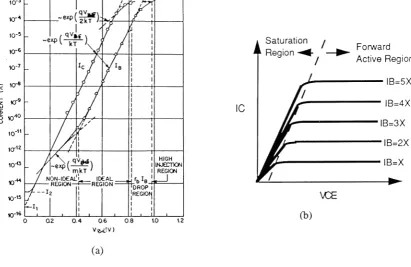
FTGTTRFS-2.1 Standard NPN bipolar transistor symbols and nomenclatures 2.2a Typical NPN Gummel plot
2.2b Typical NPN IC versus VCE plot
2.3 Typical BiCMOS NPN process cross section
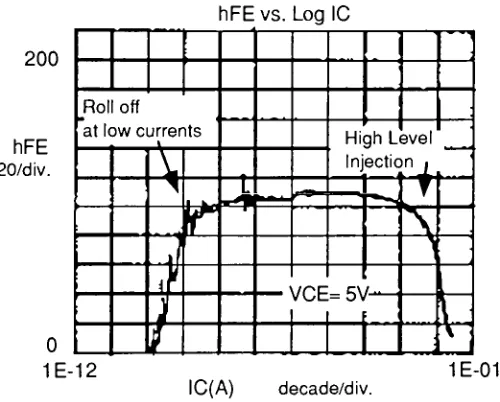
2.4 Typical plot of
hFE
versus IC2.5 Plot of NPN
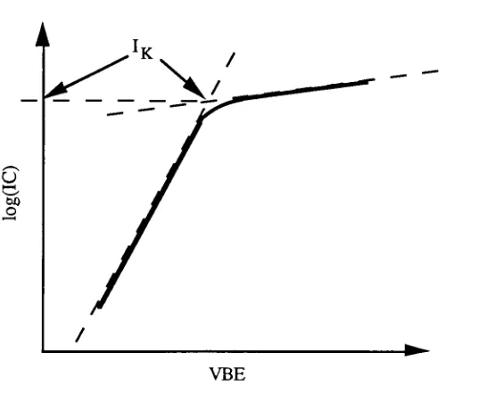
Log
IC versus VBE showing definition ofIK
2.6 NPN IC versus VCE curves showing effect ofRc
2.7 Collector Resistance schematic
2.8 NPN IC versus VCE curves showing definition of
VA
2.9 Cross section of NPN active base region, showing effect of AVCE on basewidth
2.10 Typical plot of
f-p
versus IC2.11 Critical breakdown field versus
doping
concentration 2.12 Breakdown voltages for one-sided abrupt junctions 4.1a Collector integration process flow4.1b Process cross sections for collector integration options 4.2 N-Well
doping
profiles4.3
Doping
profiles under the collector contact 4.4 Emitter integration process flow4.5 Base integration process flow
4.6 Possible intrinsic base
doping
profiles5.1 Test chip photo
6.1 1-dimensional potential versus depth for BVCEO determination 6.2 Effect of epi thickness on N-Well
doping
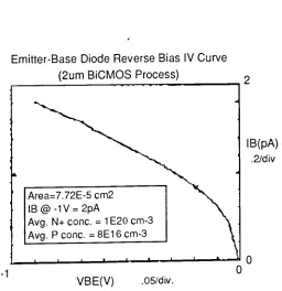
profile6.3a 2um BiCMOS emitter-base diode leakage current 6.3b 4um
BiCMOS
emitter-base diode leakage current6.4a Original 3
factor,
2 level Central Composite experiment for base option 2 6.4b Experimental design matrix for a 3factor,
2 level Central Compositedesign
6.5 Regression model for original design of base option 2 6.6 Revised Central Composite design for base option 2
7.1
hFE
versus IC for devices with a standard anneal, and an additional RTA7.2 Drain current versus gate voltage plot of NMOS devices processed with
the standard anneal and an additional RTA
7.3 IC versus VCE for NPN devices with and without DN+
7.4 Drain current versus gate voltage for PMOS devices processed with
various epi thicknesses
7.5 P+ S/D to N-Well breakdwon voltage measurments versus epi thickness
7.6a NMOS ID versus VDS curves for baseline
device,
and devices processedusing base integration options
7.6b NMOS ID versus VG curves for baseline device, and devices processed
using base integration options
7.6c PMOS ID versus VDS curves for baseline
device,
and devices processedusing base integration options
7.6d PMOS ID versus VG curves for baseline device, and devices processed
using base integration options.
7.7a
hFE
versus IC base integration option2,
with and without an additionalanneal
7.7b
hpE
versus IC base integration option2,
with and without an additionalanneal
7.8 BVCEO versus epi thickness
7.9 NMOS transconductance shift versus channel hot electron stress time
7.10a 1MHz CV measurments for
baseline,
base option 3 and base option 47.10b lOKHz CV measurments for baseline, base option 3 and base option 4
7.10c CT measurments for baseline, base option 3 and base option 4
7.11 Gated diode measurments for
baseline,
base option 3 and base option 4 A.lhpE
measurment methodA.2
Rc
measurment methodA. 3
VA
measurment methodA. 4
Ij
measurment methodLIST OF SYMBOLS; A
AE
A/D al a3 0 a-p BiCMOS bl b3 BVCBOBVCBO,
BVCEO BVCES BVEBO CCe
CMOS CT CVDn
D Pi Area Emitter AreaAnalog
to Digital converterratio of width of the bottom rectangle in Figure 2.7 to the width of
the emitter
similar to al in Figure
2.7,
except for the region under the collectorcontact
Common base current gain of an NPN transistor
Base transport factor for an NPN transistor
Bipolar-CMOS
ratio of length of the bottom rectangle in Figure 2.7 to the length of
the emitter
similar to bl in Figure
2.7,
except for the region under the collectorcontact
Curvature limited collector to base breakdown voltage for an NPN
transistor with the emitter open
Breakdown voltage of a planar junction
having
thedoping
profile ofthe base-collector region under the emitter, with the emitter open
NPN transistor collector to emitter breakdown voltage with the base
lead open
NPN transistor collector to emitter breakdown voltage with the base
lead shorted to ground
NPN transistor emitter to base breakdown voltage with the collector
lead open
Degrees Celsius
Emitter capacitance
Collector capacitance
p-n junction capacitance
Any
parasitic capacitance tied to the base of an NPN transistorComplementary
Metal-Oxide-SemiconductorCapacitance-time Capacitance-voltage
Diffusivity
of electrons in the base of an NPN transistorDN+
Deep
N+ plug diffusionDSP Digital Signal Processor
AVCB Change in VCB
AWB
Change in base widthAxb
Change in the width of the base depletion regionAxbc
Change in the width of the base-collector depletion region%bi
Built in electric field from the basedoping
profileo
Electric field as a result of minority carrier injection into the base^1
Critical electric field required to produce breakdown in a one-sidedabrupt p-n junction
esj Dielectric permittivity of silicon
fp
Unity
gainfrequency
of an NPN transistory Emitter efficiency of an NPN transistor
hpg
Common emitter configuration current gain of an NPN transistorIB NPN base current
IC NPN collector current
IE NPN emitter current
Ij(
NPN knee current^GEN
Reverse bias generation currentI5
p-n junction saturation currentIj Collector current where onset of high level injection effects occurs
due to base pushout
k
Boltzman constantLg
Diffusion length of minority carriers in the base of an NPNtransistor
Lp
Diffusion length of minority carriers in the emitter of an NPNtransistor
LI Emitter length
L2 Subcollector length
L3 Length of collector contact
M Collector Multiplication Factor
NA
Acceptordoping
density
NAB
Acceptordoping density
in the base of an NPN transistorND
Donordoping
density
NDmin
NMOS NPN N-Well N+ S/D ninib
nie T| PMOS P+ S/D?bi
Qb
qRc
RTA rcl rc2 rc3 re Pi ps2 P3 SE T Tl T3 xb xc T'c xecMinimum donor
doping density
in the collector region under theactive base
N-channel Metal-Oxide-Semiconductor transistor
NPN bipolar transistor N-type well diffusion
Heavily
doped N-type source and drain of an NMOS transistor Intrinsic carrier concentration in siliconIntrinsic carrier concentration in the base of an NPN Intrinsic carrier concentration in the emitter of an NPN
Constant used in
determining
electric field effect on xbP-channel Metal-Oxide-Semiconductor transistor
Heavily
doped P-type source and drain of a PMOS transistorBuilt in potential of a p-n junction
Charge stored in the base of an NPN
Charge of an electron
Collector resistance
Rapid Thermal Anneal
Component of collector resistance from the base to the subcollector
Subcollector component of collector resistance
Collector contact region component of collector resistance
Emitter resistance
Average resistivity of the
lightly
doped collector region under thebase of an NPN
Sheet resistance of the subcollector
Average resistivity of the collector region under the collector contact
Emitter size
Temperature
Thickness of the
lightly
doped collector region under the base of anNPN
Thickness of the collector region under the collector contact
NPN base charging time
NPN collector depletion region transit time
NPN collector charging time
NPN emitter to collector
delay
timeTp
Minority
carrier lifetime in the neutral emitterto Generation lifetime in the depletion region
VA
Early
VoltageVBE Voltage applied between the base and emitter
VCB Voltage applied between the collector and base
VCE Voltage applied between the collector and emitter
VLSI
Very
Large Scale IntegrationVj
Scattering
limited velocity of electrons in siliconum Micron
ub
Minority
carrier mobility in the basexb Depletion region width in the base
xbc Base-collector depletion region width
xc Base-collector depletion region width
x^ Depletion region width of a p-n junction
WEPI Width of the
lightly
doped collector region under the baseWc
Width of the collector region under the base Wl Emitter layout widthW2 Subcollector layout width
I. INTRODUCTION/ OBJECTIVE:
Electronic
imaging
systems require a large variety of both analog and digital signal processing techniques and circuits. These include clock generators anddrivers,
sample and hold circuits,A/D's,
memory,log
and anti-log circuits, and flexible I/O.1In order to reduce cost and size, and improve reliability of
electronic
imaging
systems, it is desirable to be able to integrate many or all of these functions on a single chip. BiCMOS process technology provides thismixed analog/digital capability.2
Due to the speed and logic
density
required, the intended applications andsystems cannot be practically realized with the existing 4um BiCMOS process.
The device speed and logic
density
of a 2um process technology is required. Much of the digital circuit design and characterization work has beencompleted in the existing 2um CMOS process. An extensive
library
of digitallogic cells and macrocells is in place and has been used to realize DSP circuits
and systems.
In order to utilize the design
library
generated, the 2um BiCMOS process mustbe modular in the sense that it is created
by
insertion of a module, or set ofsteps, into the baseline 2um CMOS process. The resulting BiCMOS process must
remain compatible with the existing baseline design rules, and the CMOS
device characteristics must be the same as those in the baseline process. In
order to mimimize development time and cost, as well as production costs, the
BiCMOS process must also be realized
by
a minimum number of additionalprocess steps and time, and use existing manufacturing equipment and
operations.
The process development procedure and results are presented. First NPN
device requirements obtained from system and circuit designers are provided.
Process integration options are introduced and evaluated for compliance with
the modularity, device performance, and cost criteria. Next, device model
approach, potential integration options are then examined to determine
attainable NPN performance. Results from fabrication experiments are
presented and
discussed,
demonstrating
2 alternatives for the NPNintegration.
II. LITERATURE REVIEW:
A. BICMOS PROCESS INTEGRATION:
BiCMOS process development has been underway for more than 22 years.
Early
efforts were ledby
RCA with the first BiCMOS publication in 1969, and work reported in the early 1970'sdealing
primarily with metal gate CMOS-Bipolar operational amplifiers.3-4The focus shifted in the mid 70's and early 80's to
smart power devices and applications. Texas Instruments, Motorola, General Electric and others published work in this area.5>6.7
The first papers
dealing
with integration of VLSI CMOS and bipolar devices appeared in 1983 to1984.-"'10,2 At
that time 2um BiCMOS processes were introduced for high speed logic and gate array families. Since then, scaled BiCMOS processes have
been reported in the literature, with 1.3um, lum, .8um and .5um published in
1985,
1985,
1987, and 1989 respectively.11.12,13.2Applications have broadened into high speed memories, mixed analog and digital circuits, and more.1 4
Specific process integration approaches have varied greatly,
depending
onthe intended application, and the process technologies already in place. The end result however, has always been to marry the strengths of CMOS and bipolar on a single integrated circuit.
B. REVIEW OFBIPOLAR DEVICETHEORY:
Collector
(N)
Base
(P)
o
O i o
fTt'
, O
^ VCE
t
VBE
Emitter
(N+)
r
V
[
o 1 o
(a)
(b)
Figure 2.1
-Standardsymbols and nomenclaturesforanNPNtransistor. Voltages in
(b)
areforthecommon emitter configuration.
The DC characteristics of this device can be derived from p-n junction theory. The expressions for terminal currents in the forward active region are given by,16
*><.*W)
u
=IB
qAEDnniz
Qb
IC"FE
IE=IC+IB
(2.1)
(2.2)
(2.3)
(2.4)
where q is the electron charge, VBE is the potential applied between the
emitter and the
base,
k is the boltzman constant, T is the temperature, A is theemitter area,
Dn
is thediffusivity
of electrons in thebase,
nj is the intrinsic carrier concentration in silicon,Qb
is the total charge in thebase,
andhpE
is the common emitter current gain.0.4 0.6 0.8
(a)
Saturation
Region-^
IC
VCE
(b)
Forward
Active Region
Figure 2.2- Typicaltransfer
curvesforan NPN transistorinthecommon emitter configuration:
(a)
Gummelplot;
log(IC)
andlog(IB)
vs.VBE foroneVCE,(b)
ICvs.VCE.A cross section of a typical NPN in a BiCMOS process is shown in Figure 2.3.2
Field Oxide
Collector Contact
Base Emitter
Contact Contact Metallization
N+S/D
(Collector)
P+S/D ixtrinsic
Base)
N+S/D
Emitter)
^
3 P Intrinsic Base/
P Substrate
N-Well
[image:18.536.65.477.26.293.2](Collector)
Figure 2.3
The NPN transistor can be described
by
a set of device parameters that are useful for circuit design and analysis.19 Theparameters pertinent to this work are presented here.
1. Current Gain:
The common emitter current gain, referred to as
lipp,
is defined as,20. 3IC o
hFE=TT^
=-i
(2-5)dIB
1-afj
where, an is the common base current gain and is defined as,20
a0=yaTM
=yaT . (2.6)
a-p is called the base transport
factor,
and is defined as,2*-*w2 _ incremental electron current reaching the collector
_ , "B ._ . OCp=
= i \Z.I)
incremental electron current from the emitter 9T2
LB
=</d~t; (2.7.1)
where W is the width of the
base,
L is the diffusion length of minority carriers in thebase,
and Tn is the electron lifetime in the base region.Thus,
the basetransport factor is a function of the base
doping
level and the minority carrier lifetime in the base.y is called emitter efficiency, and is defined as,2^
2
incremental electron current from the emitter ,
^pniE^AB^B
,Y= =1
-(2.8) total emitter current
Dni&NDELE
LE=VrV^
(281)
base,
NAB
is thedoping
concentration in the base,NDE
*s tnedoping
concentration in the emitter,
LE
is the diffusion length of holes in the emitter,and
Tp
is the lifetime of holes in the emitter. Emitter efficiency is a functionof the
doping
level,
and minority carrier lifetime in the emitter.A typical plot of
hpE
as a function of collector current is provided in Figure2.4.21
At low collector currents, the current gain can be degraded as a result
of recombination-generation current in the emitter-base depletion region, or
surface leakage current.21
At high current levels
hFE
begins to decrease dueto high level injection effects in the base or the collector.2 1
200
hFE 20/div.
hFEvs. LogIC
--1
Rolloff
atlowcurrents
High Level
\
Injection iJ
L
7
p
J
,FvCE=5\/ ..
J
{
/
E
\1E-12
[image:20.536.143.393.273.474.2]IC(A)
decade/div.Figure 2.4- Typical
plot of
hpE
vs. collector current.1E-01
The value of
hpE
affects circuit characteristics such as voltage gain of commonemitter amplifiers, and output impedance of cascode current sources.22
2. Knee Current:
As indicated in the discussion above, current gain begins to decrease at higher
collector current due to high level injection effects. These can occur in either
Figure 2.2.21 In
modern bipolar transistors, transistion into the high level
injection region is
typically
determinedby
the minimumdoping
level in thecollector. This phenomenon is referred to as the Kirk effect, or base pushoui. It can be shown that the onset of high level injection due to base push-out is
approximated by,23
*1
=qNDmin vl (2.9)
The knee current,
IK,
is a parameter used to characterize the collector curren;where this transition into the high level injection region occurs. This is
shown in Figure 2.524
VBE
Figure2.5
-Log
ICvs. VBEplot showingdefinitionof l. Notethatl
>l-|
3. Collector Resistance:
Rq
is resistance encountered as electrons flow from the emitter to the [image:21.536.145.418.279.500.2]slope=R.
IC
NPN1
-NPN2
RCNPN1 > RCNPN2
VCE
Figure2.6 - NPN IC
vsVCEplotshowingtheeffectofseriescollector resistance.
Rq
is important to consider in highfrequency
circuits as well as inapplications where a low resistance is needed.26 This
resistance can be
approximated using Equation 2.10 and Figure 2.7.27
Rc
=rcl +rc2 +rc3(2.10)
rcl=
i
2!
plTl bl
W1L1 al-bl
.
^L2
rc2=ps2w
(2.11)
(2.12)
rc3=
1
*L
p3T3 b3
W3 L3 a3-b3
(2.13)
where, rl is the resistivity of the
lightly
doped collector region under theactive base, Tl is the thickness of the
lightly
doped collector region under theactive
base,
Wl is the width of the emitter, LI is the length of the emitter, al isthe ratio of the width of the bottom rectangle, (indicated
by
the dashed lines inbottom rectangle, (indicated
by
the dashed lines in Figure2.7),
to the length ofthe emitter, rs2 is the sheet resistance of the subcollector, W2 is the width of
the subcollector, L2 is the length of the subcollector, and r3,T3,a3, and b3 are as stated for rl,Tl,al,bl for the area under collector contact.
/ f * t w
\ \ \ \ \1 ? ///_, N \ N \ \\.
/ S / S /\ \ \ \ \ \
s s s s s \ \ y, \ \ \
s / s s s \ \ \ \ X s s s s
\ \ \ \ / ? X / / \ \ \ \ \ //???? \ \ \ \ \ \
jQQQQQttagy/ / / / ? ? * P^,,U^*^t^ VTTT '- \ \ \ \ \ '- \ '- \ \ \ \ \ \ \ '- \ ^ '- * V V 5 rTTTTx \ \ \ \ \ \
Figure 2.7- Collectorresistanceschematic
4. Early Voltage:
The
Early
Voltage,V^
, is a parameter used to characterize the change inIC
Early
Voltage("
\)
0 VCE +
Figure 2.8- Ouput
characteristicsof common emitterNPN transistor, showingchange ofICwith
increasing
VCE,
anddefinitionofEarly
Voltage.With VBE constant, any change in VCE will result in an equal change in VCB.
As VCB
increases,
the base-collector depletion region will widen and the basewidth,
WB,
will decreaseby
Axb.29 This is depicted in Figure 2.9.29 The changein base-collector depletion region width, Axbc, change in base depletion
region width, Axb, and the change in base width,
AWB
are givenby
Equations2.14,
2.15 and 2.16.30Axbc
=2esi(NA
+ND
"^
Kh^
NAN(Om-avcb)
A^DrNAND^
kT<t>bi
= YlnND
Axb
= Axbc^- =AWB
(2.14)
(2.15)
(2.16)
SIC
5VCE
^ADnnP
/qVBE^
dQs
6XP1
kTJdVCE
-IC
dWB
Qb
dVCEWB
dVCB(2.17)
for a uniform base NPN transistor. From Figure
2.8,
VA
is given by,32VA IC
{
5IC
"l
1
8VCE
J
(2.18)
Examination of Equations 2.14 through 2.17 indicates that
VA
is a function ofthe base and collector
doping
profiles. For a given base profile,VA
willdecrease with
increasing
collector doping. For a given collectordoping
profile,
VA
will increase withincreasing
base doping.VCE2>VCE1
SSSSSSSSSSSSfSSS/S/S/S SSSSS/SSSSSS/S//SS///S.
1
f s f t / # j s\-mittfir * * t f * * * * * t\ % \ \ \
\ \ \ \' ... X\\\\XXX\\ :s/ss/sssHmiTTAr **********
Figure 2.9- Crosssection ofNPN active base
region,showingtheeffectof
increasing
VCEonbasewidth.
A large
Early
Voltage is important in analog circuits where a high small signaloutput resistance is required, such as active load current
5. Unity Gain Frequency:
The unity gain
frequency,
fT,
is defined as thefrequency
of operation wherehEE
is equal to one.37This
frequency
is a function of thedelay
time, xec,encountered as carriers flow from the emitter to the collector.34
fT
=1
271T0
(2.19)
This
delay
is comprised of four components; the emitter depletion-layercharging time, xe, the base charging time, xb, the collector depletion-layer
transit time, tc, and the collector charging time, t'c.34
These are a function of
the physical structure of the transistor and are given
by
Equations 2.20-2.25.34
Xec
=Te
+Tb
+Xc
+T(
(2.20)
xe
is the emitter depletion layer charging time and is givenby,
Te
=re(Ce+
Cc
+Cp)
(2.21)
where re is the small signal emitter resistance,
Ce
is the emitter capacitance,Cc
is the collector capacitance, and
Cp
is any other parasitic capacitance tied tothe base.
Tb
is the base charging time and is givenby,
V
Ti~2 1+ ;
^c
2Dn
uBWB
(2.22)
where c;bi is the built in electric field produced
by
the basedoping
profile, andub is the electron mobility in the base.
transit time and is given
by,
tc
is the collector depletion layer*c
=xc-Wc
2v,
(2.24)
where xc is the collector depletion layer width, and
Wc
is the collector width.x'c is the collector charging time and is given
by,
T'c
-RCCC
(2.25)
It is evident that to increase
fj,
the base width and collector width should bedecreased,
emitter and collector resistance should bedecreased,
and allparasitic capacitances should be decreased. A typical
fj
versus collectorcurrent curve is shown in Figure 2.10.34
o o
-4 - fT
N
3 -I
o
- 1-2
-1
-0
-to
o
in
o o
CO
o
CNJ o
IC(A)
Figure2.10- Typical
f-p
affects circuit speed performance measures such as the gain bandwidth ofamplifiers.38
6. Maximum Voltage Limitations:
a. Collector to Base:
The maximum voltage that can be applied between the collector and the base is
usually determined
by
the breakdown voltage of the collector-base junction.This maximum voltage is referred to as BVCBO, the collector to base breakdown
voltage with the emitter open.36 This breakdown
voltage is typically due to
avalanche breakdown.36 Avalanche breakdown occurs when the electric
field is high enough to impart sufficient energy to free carriers within the
depletion region, for them to break covalent bonds
during
collision with the lattice.37 Thiscreates two additional carriers that can subsequently undergo
the same process, thus producing a sudden multiplication of free carriers.37 it
can be shown that the breakdown voltage for one-sided abrupt p+n junction
can be approximated by,37
BV=
fri
2qND
(2.26)
where
1
is the electric field required to produce avalanche multiplication.A plot showing the critical electric
field,
1,
as a function ofdoping
concentration is shown in Figure 2.11.37
i i 11 i n-n i rr _
io'
tr i
r-m i ttti
E u >
10' 10 10'6 10"
Concentration N (cm-3,)
The electric field will be affected
by
the shape of the diffused junction.37 As aresult of the junction curvature the electric field increases and the breakdown voltage decreases.37 Figure 2.12 shows the breakdown voltages for
one-sided step junctions as a function of
doping
concentration and junction depth.37BREAKDOWN VOLTAGE OF PLANAR SILICON ONE-SIDED STEP JUNCTIONS
' ' ' ' '10'S ' ' 10"
BackgroundConcentration,Cg(atoms/cm )
b. Collector to
Emitter;
The maximum voltage that can be applied between the collector and the
emitter is given
by
two breakdown voltages, the collector to emitterbreakdown voltage with the base shorted,
BVCES,
and the collector to emitterbreakdown voltage with the base open, BVCEO.38 BVCES is usually equal to
BVCBO.38
BVCEO can occur either due to avalanche breakdown or due to
punch-through.39
Avalanche induced BVCEO is given by,
BVCBCL, BVCEO=
^
(2.27)
(hFE+
l)nwhere
BVCBOpi
is the planar breakdown voltage of the collector-basejunction,
and n is
typically
near 4.38Punch-through occurs when the base-collector depletion region reaches
through the base to the emitter-base depletion region, before the planar
collector-base junction can avalanche.39
This can occur if the
lightly
dopedcollector region is narrow, or the base is
lightly
doped.c. Emitter to Base:
The emitter to base breakdown voltage with the collector open,
BVEBO,
typically
determines the maximum voltage that can be applied between theemitter and the base.40 This breakdown voltage can be due to the avalanche
effect or tunneling.40
Tunneling
dominates inheavily
doped junctionswhere the potential barrier under reverse bias becomes narrow enough that
tunneling of electrons from the valence band to the conduction band can
occur.41
This mechanism dominates for breakdown voltages less than 6.2V.41
Since the emitter is typically very
heavily
doped,
care must be taken in baseIII. NPN DEVICE
TARCFTS-Device parameter targets for the NPN transistor were solicited from the system
and circuit design groups. The targets provided were based upon specific
applications of
interest,
and the subsequent circuit and device performancerequired to realize system specifications. The resulting transistor parameter
needs are shown in Table
3.1,
along with device parameters from publishedresults on similar BiCMOS processes.
fT
was stated as the primary target due torequired circuit speed performance.
TABLE
3.1
-NPN PARAMETER TARGETS
Source SE
urn x urn
hFE
fT
vA
(volts)
Ik
(mA)
Rc
(ohms)
BVCEO
(volts)
BVCBO
(volts)
BVEBO
(volts)
Refer.
DEC 2 x 30 130 16.8 9
EXAR 250 2.0 >20 42
Hitachi 2x5 100 3.8 120 8.6 10
Motorola 2.5 x 7 100 3.0 1.7 500 5.5 8
Tl 100 4.0 10 26 6.5 43
Toshiba 4.5 x 7.5 100 2.6 10 16 35 11 2
This Work
4.5 x 6 >100*
>3.0 >50 >3.0 <350 >12 -15 >12-15 >5
* valid for IC down to at least 100 nA
IV. PROCESS INTEGRATION OPTIONS:
With NPN device parameter targets established, options for integration of this
device into the existing 2um N-Well CMOS process were assessed using the
criteria of process modularity, process complexity, process compatibility with
existing manufacturing operations and equipment, and realization of the
specified NPN characteristics. In the
following
sections, process integrationalternatives are introduced, the potential compliance with device parameter
targets evaluated, advantages and disadvantages of each
discussed,
andfinally,
some alternatives chosen for further process and device design simulations
A.COLLECTORINTFOR ATION OPTIONS:
In order to maintain process modularity, the NPN collector must be created
without significantly affecting the thermal
history
ordoping
profiles of theCMOS devices. Given this constraint, and that imposed
by
use of existingfabrication equipment, eight options were identified for collector integration.
These are listed below and depicted in Figure 4.1.
1. Use existing N-Well
2. Use existing N-Well plus
Deep
N+ plug,(DN+)3. Use additional N-Well for NPN only
4. Use additional N-Well plus DN+
5. Use existing N-Well plus a
Subcollector,(SC)
6. Use existing N-Well, SC and DN+
7. Use additional N-Well and SC
8. Use additional N-Well, SC and DN+
1. Option 1-
Existing
N-Well:The exisiting N-Well profile is shown in Figure 4.2. The surface concentration
is 8xl0l->
cm'3, the junction depth is 4.6um, and the sheet resistance is 3400
ohms per square. The P+ S/D for the 2um CMOS process has a junction depth of
0.56um. The P+ to N-Well breakdown voltage is 3337,44
Consequently,
theBVCBO requirement can be met with the exsiting N-Well, provided the base of
the NPN has a junction depth or effective radius of curvature, that is not
significantly less than that for the P+ S/D. This option requires no additional
masks or process steps. The collector resistance provided
by
this option can beI
P-substrateSubcollector
Pattern,
Implant& Drive3
(option5-8) 5Epi Depositions (option 5-8)N-Well Pattern& Implant
TTUlUUmTUUHnmTtTU!.mTUUUl
Additional N-Well Patttern & Implant (option3,4,6,8)
Deep
N+Plug
Pattern& Implant^
(option2,4,7,8) N-Well Drive|
NitrideAcitveAreaPattern & Etch |P-fieldPattern & Implant
Anneal& Field Oxidation Nitride Etch & Kooi Oxidation Anti-Punchthrough Pattern & Implant
Gate Oxidation
[ThresholdAdjust Implant Gate Restore Anneal
Poly
Deposition, Dope,Pattern &Etch N+Source/Drain(alsoserves ascollectorcontact)
LTO Deposition P+ Source/Drain
BPSG Deposition
Final Anneal & BPSG Reflow Double Level MetaltoEndofProcess
j|
|
=CMOSbaseprocess=AdditionalNPNprocesssteps
Process Cross Sections
for
Collector Integration Options
Options 1-4:
ssssss/s/s////////. \ \ \ \ \ \ \
\\\\\\\\\\\S\\\ ***************************** s / s s ************** ***************************
v V . V V , ^ \ v. . VV^VVVVV^
Options5-8:
options5&7
options6 &8
p-substrate
17 1
Existing
N-WellAdditional N-Well
0 .7 1.4 2.1 2.8 3.5 4.'2 4.9 5.6 6.3 7.0
Depth(um)
Figure 4.2- N-Well
doping
profilesUsing
a minimum geometry transistor, this option will provide a collectorresistance of approximately 3803 ohms. Details of this calculation are shown
in Table 4.1.
The onset of high level injection effects at the collector will occur at a
collector current, II, approximated
by
Equation 2.9.23Assuming
an active base junction depth of 0.3 to 0.6 um,IK
for this option will be at least 3.84 mA.Details of this calculation are shown in Table 4.2.
All of the above results are summarized in Table 4.3.
2. Option 2-
Existing
N-Well with aDeep
N+ Plug:The DN+ plug serves to reduce the collector resistance as well as suppress
must be formed
by
an additional implant and the existing thermal steps. It isdesirable to have the junction depth of the plug very close to that of the
N-Well to minimize collector resistance. This option requires 1 additional mask
and
lithography
sequence, and 1 additional process step; an implant.The collector resistance can be estimated similarly to that of option 1. Details
are provided in Table 4.1. A possible DN+ plug
doping
profile is shown infigure 4.3. This option will provide a collector resistance of approximately
3348 ohms.
Using
Equation2.9,
IK
for option 2 is at least 3.84 mA, (see Table4.2).
All of the above results are summarized in Table 4.3.
3. Option 3- Additional N-Well:
The maximum N-Well
doping
level will be constrainedby
the NPN breakdownvoltages.
Assuming
that the active base junction depth will be on the order of0.3 to 0.6 um, using Figure 2.11, the N-Well surface concentration must be less
than approximately 3x10^ cm~3 in order to provide
a BVCBO greater than 15
volts. In order to maintain process modularity, it is desirable to create the
additional N-Well
by
a separate implant and the baseline process thermal steps.The lowest sheet resistance possible is obtained
by
using the existing N-Welldrive. SUPREM-34^
simulations were carried out to determine the dose
required for this implant to produce a surface concentration of 3x10*" cm"3.
The resulting N-Well with a junction depth of
6.8um,
and sheet resistance of600 ohms per square, is shown in Figure 4.2. This process option requires 1
additional mask and 3 additional process steps; a photoresist strip, an
implant,
and a clean cycle.
Using
Equation2.10,
the minimum collector resistance obtainableby
option 3 is approximately 952 ohms,(see Table 4.1).Using
Equation2.9,
IK
for option 3 isat least 7.68 mA, (see Table 4.2).
21 -T
ro i
E
o
c o
c
<X>
o c o o
Collector
Doping
Profiles0 1 2 3
Depth(um)
Figure 4.3
-Doping
profile underthecollector contact4. Option 4- Additional N-Well and
Deep
N+ Plug:This option will require 2 additional masks, and 4 additional process steps. The
Using
Equation2.10,
the lowest obtainable collector resistance for this option is approximately 770 ohms,(see Table 4.1). TheIK
for this option is at least 7.68mA,(see Table 4.2).
All of the above results are summarized in Table 4.3
5. Option
5-Existing
N-Well and Subcollector:The subcollector serves to lower the collector resistance of the NPN and
improve
latch-up
immunity
of the CMOS.2,8 Given the condition of usingexisting fabrication equipment and manufacturing operations, subcollector
formation
by
implantation into a p-type substrate, and depostion of a p-typeepitaxial
layer,
was chosen. The resistivity of the epitaxial layer must be thesame as the CMOS substrate resistivity in order to maintain process modularity.
The thickness of the epitaxial layer will be determined
by
the breakdownvoltage,
fj,
andV^
requirements of the NPN,by
the requirement that theN-Well and subcollector merge to form a continuous N-type region, and
by
therequirement that the PMOS device parameters remain the same as produced
by
the baseline 2um CMOS process.47
If the optimum condtions for the NPN are
incompatible with those required
by
the PMOSdevice,
then the subcollectorcan be implemented exclusively in the NPN region, or a separate N-Well can be
used for the NPN. This option will require 1 additional mask step, and 6
additional process steps; 2 furnace oxidations, an implant, an epi
deposition,
aphotoresist strip, and a clean.
The collector resistance for this option is approximately 628 ohms,(see Table
4.1).
Ij
for this option is estimated to be 4.61 mA,(see Table 4.2).6.
Option 6- Existing N-Well.Subcollector.and
Deep
N+ Plug:This option will require 2 additional masks, and 7 additional process steps. The
resulting collector resistance will be approximately 406 ohms,(see Table 4.1).
Ij
will be on the order of 4.61 mA,(see Table 4.2).All of the above results are summarized in Table 4.3.
7. Option 7-Additional N-Well with a Subcollector:
This option requires 2 additional masks, and 9 additional process steps. The
minimum collector resistance is on the order of 260 ohms,(see Table 4.1).
Ij
isapproximately 7.68 mA,(see Table
4.2)
These results are summarized in Table 4.3.
8. Option 8-Additional N-Well with a Subcollector and
Deep
N+ Plug:This option requires 3 additional masks and, 10 additional process steps.
Rc
isapproximately 172 ohms,(see Table 4.1).
Ij
is on the order of 7.68 mA,(see Table4.2)
All of the above results are summarized in Table 4.3.
9. Option Chosen for Further Evaluation:
It is evident from the results shown in Table
4.3,
that regardless of the N-Wellchosen, a subcollector is necessary in order to meet the collector resistance
target. In addition, the collector resistance and knee current requirements
should be realizable
by
the use of a subcollector, DN+, and the existing N-Well.Based upon these results, and the extra process steps required for the
additional N-Well, a decision was made to investigate option 5 and 6
first,
andpursue options 7 and 8 only if there were conflicts between optimum
conditions to satisfy the NPN and PMOS requirements, or if compliance with
TABLE 4.1
-COLLECTOR
RESISTANCE
CALCULATIONS
Option
Rc
(ohms)
rcl
(ohms)
rc2
(ohms)
rc3
(ohms)
pi ps2
(ohm-cm) (ohm-cm)
p3
(ohm-cm)
Tl
(um)
T3
(um)
1 3803 780 2550 473 2 3400 2 4.1 4.1
2 3348 780 2550 19 2 3400 .08 4.1 4.1
5 628 382 15 231 2 20 2 2 2
6 406 382 15 9 2 20 .08 2 2
3 952 312 450 190 .8 600 .8 4.1 4.1
4 770 312 450 8 .8 600 .08 4.1 4.1
7 260 153 15 92 .8 20 .8 2 2
8 172 153 15 4 .8 20 .08 2 2
Noiej.
For all options,Wl=8um,
Ll=6um,
al=2.025,bl=2.37, W2=28um, L2=21um,
W3=15um,
L3=6um,
a3=1.54, b3=2.37TABLE
4.2-Ii
CALCULATIONS
Option
il
(mA)
NDmin
(atoms/cm-3)
1
3.84
5
x 10152
3.84
5
x 10153
7.68
1 x 10¹⁶
4
7.68
1
x 10l6
5
4.61
6
x 10156
4.61
6
x 10157
7.68
1
x 1016
8
7.68
1
x 1016TABLE 4.3
-C0L1..ECTORINTEGRATION OPTIONS
SUMMARYOption
Re
h
ExtraMasks
Extra Steps
Comments
1
Existing
N-Well3803 3.84 0 0 Can meet BV needs. Should meet
IK
needs.Rc
too high. 2Existing
N-Welland DN+
3348 3.84 1 1 Can meet BV needs. Should meet
Ik
needs.Rc
too high.3
Added N-Well
952 7.68 1 3 Can meet BV &
Ij,^
needs.Rc
toohigh.
4
Added N-Well
and DN+
770 7.68 2 4 Can meet BV &
1^
needs.Rc
toohigh.
5
Existing
N-Welland SC
628 4.61 1 6 Can meet BV &
1^
needs.May
notmeet
Rc
needs.6
Existing
N-WellSC and DN+
406 4.61 2 7 Should meet all needs.
7
Added N-Well
and SC
260 7.68 2 9 Should meet all needs.
8
Added
N-Well,
SC and DN+
172 7.68 3 10 Should meet all needs.
B. EMITTER INTEGRATION OPTIONS:
Given the previously stated restrictions, 3 options were identified for emitter
formation. These are listed below and depicted in Figure 4.4.
1. Use N+ S/D implant as emitter
2. Use additional emitter mask; either open or not for N+ S/D implant
P-substrate
N-WellPattern & Implant
N-WellDrive
Nitride Deposition
Acitve Area Pattern & Etch
|P-fieldPattern & Implant
Anneal& Field Oxidation
NitrideEtch & Kooi Oxidation
Anti-PunchthroughPattern & Implant
GateOxidation
ThresholdAdjust Implant
Gate Restore Anneal
iPolysilicon EmitterProcess (Option3)
Poly
Deposition,Dope.Pattern & EtchlAdditional Emitter Maskand Implant
|
=CMOS baselineprocess|
=Additional NPNsteps(Option2)
N+ Source/Drain (Also Emitter Implant- Option
1)
LTO Deposition
P+ Source/Drain
BPSG Deposition
Final Anneal & BPSG Reflow
Double Level Metal to EndofProcess
Figure 4.4- Emitterintegrationoption processflow
1. Option 1- N+ S/D as Emitter:
This option requires no additional masks or process steps. Due to the high dose
used for the N+
S/D,
it may pose severe limitations on base design in order toprevent tunneling in the emitter-base junction, and
keep
BVEBO greater than5V.41
The final anneal in the 2um CMOS process is 950C for 45 minutes in a nitrogen
ambient. This may not be sufficient for complete elimination of the implant
in the emitter-base space charge region, thus producing low current
hF
Edegradation.48
Rapid thermal anneal,
(RTA),
processing has been shown tocompletely eliminate this implant damage.48 An RTA
step may be necessary to provide the low current
hFE
performance specified. However, an added RTAstep may not be compatible with the process modularity constraint.
All of the above results are summarized in Table 4.4.
2. Option 2- Additional Emitter Mask &
Implant:
An additional emitter mask and implant could be employed if option 1 could not meet device requirements due to the problems mentioned above. This option
requires 1 additional mask and 3 additional process steps; an
implant,
a photoresist strip, and a clean. It is easily implemented with existing operations and equipment, and provides a modular process.All of the above results are summarized in Table 4.4.
3. Option 3-Polysilicon Emitter:
A polysilicon emitter could be used if NPN performance requirements are not realizable with an implanted emitter.49 Due
to lack of experience with
polysilicon emitters, this option could require considerable development effort
and time. It requires at least one additional mask and may not be compatible
with maintaining process modularity. These results are summarized in Table 4.4.
TABLE
4.4
EMITTER INTEGRATION
OPTIONS SUMMARY
Option ExtraMasks Extra
Steps
Comments
1
N+ S/D
0 0 Possible low current
hFE
degradation andtunneling
problems.
2
Added Implant
1 3
Easily
implementable to overcome problems with option 1.3
Poly
Emitter>1 >4 \Io experience with poly emitters.
May
not be4,
Option Chosen for Further Evaluation:Based upon the complexity, lack of experience, development effort required,
and significant deviation from the CMOS baseline process of option
3,
theprevalent use of option 1 for similar processes reported in the literature,1 2
and subsequent lack of anticipated problems in meeting device requirements
with option
1,
option 1 was chosen for initial process and device design work.Option 2 was chosen as the alternative approach if problems were encountered
in using option 1. Due to the lack of available tools that could accurately model
RTA processes, it was decided to investigate the effect of RTA processing
empirically.
C. BASE INTEGRATION OPTIONS:
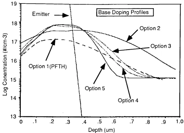
Given the previously stated restrictions, 5 options were identified for
incorporation of the base of the NPN. These are listed below and depicted in
Figure 4.5. Process simulations for each option were completed using implant
doses and energies that would supply a peak active base
doping
concentrationof lxlO1** Cm"3
at a junction depth close to that of the N+ S/D. The
corresponding
doping
profiles for each option are shown in Figure 4.6. In allinstances the P+ S/D will be used as an extrinsic base.
1. Implant intrinsic base, (IB), prior field oxidation
2. Implant IB after Kooi oxidation, and prior to gate oxidation
3. Implant IB after gate oxidation, and prior to gate restore anneal
4. Implant IB after gate restore anneal, and prior to poly deposition.
P-substrate
N-Well Pattern& Implant
N-Well Drive
|]=
Baseline CMOS Process1
=AdditionalStepsfor NPN:
P-fjela7jntrinsic BasePartern & Implant (Option 1;
Nitride Deposition
Acitve Area Pattern & Etch
P-field Pattern & Implant
Anneal& Field Oxidation
Nitride Etch& KooiOxidation
[IntrinsicBase Pattern& Implant (Option2)
Anti-PunchthroughPattern & Implant
Gate Oxidation
[Threshold Adjust Implant
I (ntrinsic BasePattern& Implant
GateRestore Anneal
Intrinsic BasePattern & Implant
(Option3)
(Option4)
Poly
Deposition, Dope,Pattern & EtchN+ Source/Drain
LTODeposition Intrinsic Base Pattern & Implant (Option5)
P+ Source/Drain
BPSG Deposition
FinalAnneal & BPSG Reflow
DoubleLevelMetalto EndofProcess
Figure 4.5
Base
Doping
ProfilesOption 2
Option 4
.4 .5 .6
Depth(um)
Figure 4.6
-Possible intrinsic base
doping
profilesi1 'i ' ' i
7 .8 .9 1.0
1. Optionl-dmplant IB prior to field oxidation):
Option 1 was chosen primarily to investigate the
feasibility
of using the P-fieldthreshold implant as an intrinsic base. The first thermal step
following
thisimplant is a nitrogen anneal, consistent with the requirement of complete
damage elimination in higher dose boron implants.^u It is necessary to move
the P-field implant prior to nitride deposition in order to place it in the active
area of the NPN. This should have no effect on the resulting CMOS device
parameters. The possibility of altering the P-field threshold dose exists, but
this may affect the junction capacitance of the NMOS device since the N+
source and drain are in contact with the P-field region. The junction
capacitance is given by,^ 1
EsiA
J Xj
(4.1)
where, xd is the N+ S/D depletion region width and is calculated
by
substitutingthe appropriate
doping
levels and applied biases in Equation 2.14. An increase [image:46.536.109.427.63.293.2]With this approach, field oxide or polysilicon can be used to provide self
alignment of the emitter and extrinsic base. This option would require no additional masks or process steps. All of the above results are summarized in Table 4.5.
2. Option 2-Implant IB prior to gate oxidation:
This option requires 1 additional mask, and 3 additional process steps; an
implant,
a photoresist strip, and a clean. One potential problem with thisoption is that the thermal step
immediately
following
the intrinsic base implant would be an oxidation. It may be necessary to insert a short nitrogenanneal step in order to completely eliminate all implant damage in the intrinsic base region.5u An additional anneal is
not desirable for maintaining
process modularity. Polysilicon can be used to provide self alignment of the
emitter and extrinsic base. All of the above results are summarized in Table 4.5.
3. Option 3-Implant IB prior to gate restore anneal:
This option requires 1 additional mask and 3 additional process steps; an
implant,
a photoresist strip and a clean. The first thermal step after theimplant is a nitrogen anneal, and polysilicon can be used to provide self
alignment of the emitter and the extrinsic base. A possible problem exists with
exposure of the gate oxide to a photoresist pattern, an implant and a
photoresist strip. This may introduce contamination, and degrade the
reliablity of the gate oxide, and subsequently that of the CMOS devices.52 All
of
the above results are summarized in Table 4.5.
4. Option 4-Implant IB prior to poly deposition:
Option 4 is identical to option 3 except that it is done after the gate restore
anneal, so there may be an even greater potential for degradation of gate oxide quality. There are no more thermal oxidations after this point in the process,
5.
Option 5-Implant intrinsic base after poly deposition;This option also requires 1 additional mask and 3 additional process steps.
Polysilicon cannot be used to provide self alignment of the emitter and
extrinsic base. The implant can be inserted either prior to or after the N+ S/D
implant. All of the above results are summarized in Table 4.5.
TABLE 4.5 INTRINSIC
BASE INTEGRATION
OPTIONS
SUMMARY
Option Extra
Masks
Extra
Steps
Comments
1
P-Field
0-1 0-3 Base anneal built in. Will have to move P-field
implant prior to nitride deposition. Change of P-field implant may be possible. Extra mask & implant
could also be used.
2
After Kooi
ox.
1 3-4 Base anneal step may need to be added. This may be
incompatible with modularity requirement.
3 After gate
ox., before
gate anneal
1 3 Base anneal built in.
May
degrade gate oxide withpattern and implant. Gate restore anneal may repair
any gate damage.
4 After gate
anneal
1 3 Base anneal built in.
May
degrade gate oxide withpattern and implant.
5
After
Poly
1 3 Base anneal built in. Polysilicon not available for
self alignment of extrinsic base and emitter.
6. Options Chosen for Further Evaluation:
V. TEST CHIP DESIGN:
A test chip was designed in order to complete fabrication experiments and
characterize process results. The design rules for the NPN were derived from
the assumptions used in
determining
the 2um CMOS rules. In some instancesvariations of specific rules were included in test structures to investigate
their effects on performance and reliability. A list of structures designed , as
well as the purpose of each is given in Table 5.1. The test chip dimensions are
5805um
by
5030um. The mask set was obtained for a lx exposure tool, andconsisted of 15
levels,
3 additional for the NPN. A picture of the test chip isshown in Figure 5.1.
_* ^""'^.""""""iiiMMiMiMHii ...,.
. ....
a i
i/ in>ipiimi#iii
::::,::::=:
i !'"'p'. #.*vt*v pjpa*vavjiM'p.1!!lliiMJ!lf&
{
n
fa aal m ; a a a
>a ad C aa aa a
-'a ai E
a^a^a ,m mmmaa uiiln aa a a a a a * i m.uiiiu a
a.ira a aa aa aa aa aa aa aa aa.[aa [aa
aaVaa.-aa^aa-Ba^ri a aa aa a
> i ii: aa aa aa !>!=< aa';aa'aaJ,-laa,=B,l> .::;':';
al.-a a aa aa aa aa aa aa aa >. iiJ Ba-;aa-;aa--aai a?:* : a aa aa a rnr u r u
ia~a"w ftiiiiiMsmiioiimonBi(iinniurii\irt,Jr'^nu"d"ii
> i
i aa
{((m:
.M^aaaaaaaaaaaaaaaaaaaaa
Figure 2.12 - Photograph
26rn-230rn
26rnil,2
26rnwl,2,3
TABLE
5.1
-TEST
CHIP STRUCTURES
Structure Name
Standard layout NPN round emitter size series. Emitter diameters
of
6,10,12,17,20,24,30,38
microns; for evaluation of NPNparameters obtained, and onset of emitter crowding. All have
subcollector and DN+. Subcollector coincident with N-Well.
6um round emitter, standard layout NPN, with subcollector inset
to
N-Well;
for evaluation of subcollector layout latitude. Description/Purpose6um round emitter, standard layout NPN, with varied N-Well to
active area spacings; for evaluation of N-Well layout latitude.
26rnwfl,2,3 Same structures as
26rnw's,
except field oxide used to provide selfalignment of base and collector.
26sn,212sn,
224sn
Standard layout square emitter NPN's, with emitter widths of 6,12
and 24 um; for evaluation of square emitter devices.
26rnx,212rnx Same as 26rn &
212rn,
except DN+ omitted26rnpf 1,2 Same as 26rn except Nwell to P-field spacing is reduced to 4um &
Oum;
for evaluation of Nwell to P-field layout latitude.26rnel-6 Same as
26rn,
except variations on extrinsic base layout rules; forevaluation of extrinsic base layout latitude.
26rnsapl-4 Same as
26rn,
except polysilicon used in transistor for selfalignment of emitter and extrinsic
base,
and as an intrinsic basefield plate.
26rnp
Poly
emitterNPN,
(via mask used for emitter area).npwrlx,2x,4x Interdigitated power npn devices
npwrlxb-4xb Same as npwr's above, except emitter ballast resistors built in.
Ipnp
1-6 Lateral PNP structures; for evaluation of parasitic lateral pnpcharacteristics as a function of layout rules.
vpnpl-6 Vertical PNP structures; for evaluation of parasitic vertical pnp characteristics as a function of layout rules.
GDl-8,GDlF-8F|Gated diodes for all diodes possible, F structures have field oxide
"fingers"
in the diode; for evaluation of dark current
characteristics of all diodes and field oxide region.
R1-R5 Structures for evaluation of sheet resistance and contact
resistance of all regions
including
pinch resistors.CMOS T1-T15 2um CMOS standard test structure set; includes
L-series, W-series,
and
latch-up
test structures.BiPMOS's Same as standard PMOS test structures, except subcollector mask
included.
BiLUT's Standard
latch-up
test structures except subcollector included.Also
latch-up
structures using DN+, and NPNlatch-up
structures.5 3
VI. PROCESS/DEVICE DESIGN AND MODELLING:
In this section, the process integration options chosen are evaluated further
for compliance with the criteria previously described. All process simulations
were done using SUPREM-3. NPN transistor simulations were done using
SEDAN-254
and BIPOLE.55 CMOS device simulations were carried out using
SUPREM-3.
A. TRANSISTORDESIGNFOR BREAKDOWN VOLTAGE:
Breakdown voltage requirements were used to provide
boundary
conditionsfor the intrinsic base and collector design.
1. BVCBO:
The curvature limited collector to base breakdown voltage is determined
primarily
by
thedoping
concentration of the N-Well and the junction depth ofthe intrinsic and extrinsic base.3 7 With use of the existing N-Well as the
collector, the N-Well
doping
profile is fixed. The present P+ to N-Wellbreakdown voltage is 33V. Hence, the 15V BVCBO target provides the limits for
the intrinsic base design. The intrinsic base must be designed such that the
critical field for avalanche breakdown is not exceeded at 15V. The 2um CMOS
P+ S/D junction depth is 0.56um.
Using
Figure2.11,
and assuming an effectivebackground N-Well concentration of 4xl015 cm"3,the effective junction depth
of the P+ S/D is lum. Given the same conditions, the minimum effective
junction depth required to maintain a BVCBO greater than 15V, is on the order
of 0.3um. Consequently, the minimum radius of curvature for the intrinsic
base junction should be greater than or equal to 0.3 times that for the P+ S/D
junction. If this limit imposes a constraint on realizing desired device targets,
the P+ S/D could be used as an extrinsic base guardring, at the expense of
increased device size and collector to base junction capacitance. This would
reduce ij.
2. BVCEO:
This breakdown will be due either to the onset of avalanche breakdown of the
planar base-collector diode, or punch-through of the
a.) Avalanche Limited Breakdown:
Avalanche limited breakdown will be given
by
the relationship in Equation2.27. To determine the minimum
BVCBOpl,
insert the minimum BVCEO and themaximum
hpg
in Equation 2.27.Assuming
n=4, and a maximumhFE
of200,
theminimum allowable
BVCBOpl
is 56.5 volts.. For maximumhFE
of150,
theminimum
BVCBOp]
is 52.5 volts.Using
Figure2.11,
this results in a maximumallowable collector
doping
concentration at the base-collector junction ofapproximately 1.3xl01(> cm~3. This will place constraints on epi thickness and
subcollector up-diffusion.
b. Punch-Through Limited Breakdown:
Base integration option 1 was chosen to investigate the limits on epi thickness
imposed
by
punch-through BVCEO. Base implant dose and energy parameterswere chosen to provide a peak active base
doping
concentration of lxl018cm~3near the N+ S/D junction depth. Subcollector implant parameters were
chosen to provide a subcollector sheet resistance of 20 ohms per square.
SEDAN-2 was used to look at the 1-dimensional potential curves for BVCEO. An
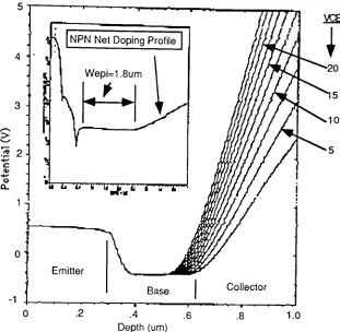
epi thickness of 7.5um was modelled . In Figure 6.1 it is seen that for this
condition the thickness of the
lightly
doped collector region is approximately1.8 um, and punch-through has not occurred at 15V. A minimum allowable epi
thickness of 5.5um was chosen as a bound for subsequent device simulations
and experiments.
3. BVEBO:
The BVEBO requirement will impose limits on the intrinsic base
doping
profile.With the
heavily
doped arsenic N+ S/D as an emitter, care must be taken in thebase design to avoid tunneling at the base-emitter junction.41 Due
to the
sensitivity of BVEBO characteristics to specific details of the intrinsic base
I I I'
I I l
4
C
o