IET Power Electronics
Research Article
Operation and control design of an
input-series–input-parallel–output-series
conversion scheme for offshore DC wind
systems
ISSN 1755-4535
Received on 9th December 2016 Revised 3rd April 2017 Accepted on 26th April 2017 doi: 10.1049/iet-pel.2016.0885 www.ietdl.org
Ahmed Darwish
1, Derrick Holliday
1, Stephen Finney
11Department of Electronic and Electrical Engineering, University of Strathclyde, Glasgow, UK
E-mail: [email protected]
Abstract: High-power converters for high-voltage direct current transmission systems and collecting networks are attracting increasing interest for application in large offshore wind farms. Offshore wind farms are capable of generating more electric energy at lower cost when compared with onshore wind systems. In this study, DC/DC voltage conversion should be achieved with a power converter that uses readily available semiconductor devices. A modular DC/DC converter can achieve the required system currents and voltages without exceeding semiconductor ratings. In this study, the operation and control strategy for an input-series–input-parallel–output-series (ISIPOS) energy conversion system for wind systems are presented. The ISIPOS system allows the direct connection of wind turbines to the DC grid. In this research, the design process to control the input and output currents and voltages is explained. In addition, a new method to ensure voltage and current sharing between the different modules is presented and explained. The basic structure, control design, and system performance are tested using MATLAB/ SIMULINK. Practical results validate the control design flexibility of the ISIPOS topology when controlled by a TMSF280335 DSP.
1 Introduction
Presently, >3000 offshore wind turbines have been installed in the European sector with total capacity of ∼11 GW. In 2015, the allocated investment for offshore wind farm projects exceeded £14bn [1]. Offshore wind farms are preferred over onshore farms for many reasons, including increased power capability, lower environmental impact and the ability to install larger wind turbines [2, 3]. Therefore, it is expected that offshore farms will form approximately one-third of the total generated wind power in the near future [2]. Thus, the international trend towards offshore wind farms necessitates long distance and large transmission networks with high power ratings.
For wind farms located >75 km offshore, advanced high-voltage direct current (HVDC) transmission systems become more promising. This is because HVDC systems require fewer transmission lines when compared with AC architectures, in addition to their stability and controllability [4]. The absence of reactive power circulation in the submarine cables of HVDC systems reduces power losses in the cables and increases the total efficiency [5]. Moreover, large-scale offshore wind power systems form weak connection points where HVDC system can assist with grid code compliance, increasing the power quality onshore and dealing with the voltage and current unbalance at high power levels [4]. Considered as important merits in weak grids, HVDC transmission systems offer the capability of black start as well as the ability to operate at relatively low wind speeds [4].
Presently, the most common configuration for offshore wind farms with an HVDC transmission network uses an AC collection network to connect all the wind turbines to an offshore AC/DC platform [6, 7]. However, this configuration has high total cost and size because it requires a bulky low-frequency AC transformer. For this reason, replacing the AC collection network with a DC network can add additional advantages. First, the circulating reactive currents will be eliminated and hence, the total efficiency will be improved. Second, DC collection networks will omit the need for the line-frequency AC transformer and hence, the total footprint of the system can be reduced. In this paper, the main challenge of this configuration would be the ability to boost the wind turbine low voltage to the desired transmission level. The
DC/DC converters proposed to achieve this should have acceptable efficiency and offer the same reliability when compared with the eliminated AC transformer [8].
Modular DC/DC converters for medium-voltage applications have been discussed extensively in the literature [9–14]. Due to their capability to operate with zero-voltage switching, phase-shift full-bridge converters are widely used for high-power applications [12]. Many configurations for parallel and series connection of several modules are proposed in order to reduce the current and voltage stresses in the semiconductor devices and hence, the device technologies that are readily available in the market can be used in the implementation. Therefore, each module is exposed to a small fraction of the total voltage and current and hence, the semiconductor devices can operate at relatively high switching frequency (> 10 kHz). In addition, the turn's ratio of the isolation transformers can be reduced if the converter outputs are series connected. This leads to a lower leakage inductance in each module. These types of DC/DC converter are suitable for both unidirectional and bidirectional power applications. Traditionally, the configurations of multi-module DC/DC converters can be classified into four main types: input-parallel–output-parallel, input-parallel–output-series (IPOS), input-series–output-parallel and input-series–output-series (ISOS) [14].
voltage ripples in the passive components can be reduced significantly when interleaved modulation of the sub-modules is used, leading to better performance. However, the control strategy of this configuration should achieve three main objectives:
i. Controlled power flow between the input and output sides while keeping the converters voltages and currents within the acceptable limits.
ii. A fast dynamic response during abnormal operating conditions.
iii. Voltage and current sharing between the different sub-modules.
Generally, two main control techniques have been used for these types of converters, namely, fixed frequency and variable frequency techniques. Variable frequency control adds to the complexity of controller design, as well as creating undesired EMI components which necessitate increased filtering [15–17]. However, fixed frequency control, such as phase-shift control (PSC) [18, 19], avoids these disadvantages and offers better performance, especially for the DC/DC converter part of the system. Using the fixed frequency control approach, this paper explains the operation and modelling of the previously mentioned ISIPOS AC/DC converter for medium-voltage applications. In addition, the paper identifies important issues in the
implementation of control algorithms to satisfy both simplicity and desired performance using classical proportional + integral (PI) control loops. The remaining of this paper is organised as follows: Section 2 describes the system under investigation and explains its basic structure and operation. Section 3 discusses the control methodologies of the system from the perspective of overall power transfer control as well as power sharing control. In power transfer control, the AC/DC rectifiers and DC/DC converter modules are considered as if their series semiconductor switches operate simultaneously, and any small voltage and current mismatches are neglected. In power sharing control, the decentralised controllers are responsible for ensuring equal power sharing between the different rectifiers and modules in order to improve the modularity and reliability. MATLAB/SIMULINK simulations for power transfer and power sharing controllers are presented in Section 3. Section 4 presents the experimental results of the ISIPOS system when controlled with a TMS320F28335 DSP.
2 System description
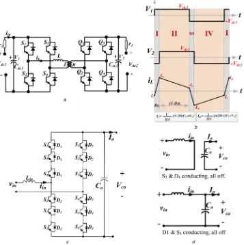
[image:2.595.107.504.51.504.2]The symbols and variables used to describe the system shown in Fig. 1a are listed in Table 1 and the overall AC/DC system is shown in Fig. 1b. For practical operation at 5 MW and a DC collecting voltage of 50 kV, the input and output currents and voltages of the system are listed in Table 2. A single rectifier with Fig. 1 ISIPOS AC/DC energy conversion system
(a) Full system, (b) Simplified AC–DC ISIPOS system, (c) Single rectifier with its DC/DC converter, (d) Simplified block diagrams of overall controllers
its DC/DC group is shown in Fig. 1c where nac is the number of
rectifiers per phase, ndc is the number of DC/DC converters per
rectifier and Ndc is the total number of DC/DC converters in the
system. For the dual-active bridge (DAB) DC/DC converter circuit, it is preferable to operate the converter in the condition that the input and output voltages are close to each other to ensure that the circulating current and the converter inductor values are as low as possible [20].
Therefore, the intermediate voltage Vm is chosen as
Vm=VNdc
dc= Vdc
3ndcnac (1)
To ensure reliable operation, the de-rating factor of the switches should be ∼70%. In view of this, the IGBT switches for the rectifiers and DC/DC converters are rated at 1.7 and 1.2 kV/200 A, respectively. The number of modules and the operating conditions
are listed in Table 3. The inductor value L is selected to transfer the module power at a duty ratio D = 0.25 while the other passive elements are chosen to allow for <10% ripple across the capacitors and inductors.
3 Control structure
Overall, the system under investigation can be viewed as a two-stage power converter, as shown in Fig. 1b. For such a system, controller design becomes complex for several reasons. The overall system bandwidth of the power transfer controller is restricted to guarantee that undesired voltages and currents at the resonance frequencies are not excited because of the existence of the resonant poles. Consequently, the dynamics and transient response of the system are limited. In addition, other control loops should be inserted to assure equal current and voltage sharing between the series and parallel modules. These loops should respond more quickly than the main power controller and should not interact with it. This adds to the complexity of the control design process. In this context, the control system can be divided into two parts:
• Overall controller which controls the power transfer from the input to the output sides and sets the operating points of the system.
• Module-based controller to ensure equal power sharing between the modules and to cater for the small mismatches in the different power modules.
The following subsections will discuss the design process for these loops in order to achieve correct operation, acceptable transients and suitable dynamic response during faults and abnormalities, as well as to achieve correct sharing between the different power modules.
3.1 Overall control
Assuming that all the passive components of the converters are identical and that all converters have the same duty ratio and gate drive signals, i.e. all the semiconductor switches are switched on and off in the same time, the equivalent circuit of the IPOS DC converter will be as the DAB circuit shown in Fig. 8a with C1 = Cdc1/ndc, C2 = ndcCdc2, and L = L/ndc. In the same way, the
equivalent circuit of the ISOS AC converter will behave as the circuit shown in Fig. 8c. In other words, the series–parallel combinations of AC and DC converters are viewed as two cascaded converters (Appendix).
3.1.1 DC converter control: The closed-loop block diagram of the overall DC converter is shown in Fig. 1d (the accompanying mathematical analysis can be found in Appendix), where
Gc1(s) = Kp1+
Ki1
s (2)
(see (3)) where d is the small-signal duty ratio of the DAB converter and D is equilibrium duty ratio where its maximum value Dmax = 0.5. To ease the gain selection process, a point at the middle
of the trajectory, D = 0.25, is selected to be the equivalent operating point. Then, the root loci of the closed-loop system can be drawn in two ways. In the first way, the proportional gain Kp1 is kept
constant at 0.5 while the integral gain Ki1 is changed in the range
of [10:50]. In the second way, Ki1 is constant at 15 and Kp1 is
changed from 0.1 to 1. The resulting loci are shown in Figs. 2a and b. The ranges of the gains are selected initially to keep the system stable. From the presented analysis, the system always has real poles and no oscillations. The controller gains are selected to be Kp1 = 0.45 and Ki1 = 25 to give acceptable dynamics and 90° phase
margin.
[image:3.595.42.290.246.645.2]3.1.2 AC converter control: Using the same approach, the equivalent circuit of the series-connected AC converters can be considered to be as shown in Fig. 8c, with Lin = nacLac and Co =
Table 1 System variables
Symbol Variable
nac number of rectifiers per phase
ndc number of DC/DC converter modules per rectifier
Ndc total number of DC/DC converter modules
vinkk ∈ {a, b, c} phase k AC voltage
iinkk ∈ {a, b, c} phase k AC current
vin_kpp ∈ {1, 2, …, nk ∈ {a, b, c}
ac}
AC voltage of the pth AC/DC rectifier in phase k
vm_kpp ∈ {1, 2, …, nk ∈ {a, b, c}
ac}
DC voltage of the pth AC/DC rectifier in phase k
Iindc_kpp ∈ {1, 2, …, nk ∈ {a, b, c}
ac}
DC current of the pth AC/DC rectifier in phase k
iindc_kp_j
k ∈ {a, b, c} p ∈ {1, 2, …, nac}
j ∈ {1, 2, …, ndc}
input current of the jth DC/DC module of the pth rectifier in phase k
vo_kp_j
k ∈ {a, b, c} p ∈ {1, 2, …, nac}
j ∈ {1, 2, …, ndc}
output voltage of the jth DC/DC module of the pth rectifier in phase k
Mod_kp_j
k ∈ {a, b, c} p ∈ {1, 2, …, nac}
j ∈ {1, 2, …, ndc}
DC/DC module number j connected to the
pth rectifier in phase k
Rec_kp
k ∈ {a, b, c} p ∈ {1, 2, …, nac}
j ∈ {1, 2, …, ndc}
AC/DC rectifier number p in phase k
Vo_kpp ∈ {1, 2, …, nk ∈ {a, b, c}
ac}
total output DC voltage of DC/DC series converters group connected to the pth
rectifier in phase k
Vo_kk ∈ {a, b, c} total output DC voltage of DC/DC series converter group in phase k
Vdc total output DC voltage
Idc output DC current
Table 2 Main characteristics of the system under consideration
Parameter Value
Prated 5 MW
vac 4 kV (line-to-line)
iin 722 A (rms)
Vdc 50 kV
Idc 100 A
[image:3.595.42.287.686.776.2]Cac/nac. Therefore, the overall AC control system can be expressed
as shown in Fig. 1d. Figs. 2c and d show the frequency domain analysis of the control loops. The gain values are selected as Kp2 =
3 and Ki2 = 15 to ensure fast response (acceptable bandwidth) and
to reduce system oscillations
Gc2(s) = Kp2+
Ki2
s (4)
Gac(s) =v~δ~co= G G14
14(1 + CoLins2) + LinsVin
where
Lin= Lac⋅ nac, Co= Cac/nac
(5)
Fig. 3a shows the MATLAB/SIMULINK simulation results for the system using these parameters and control gains. Fig. 3b shows the simulations for the case when 80% pole-to-pole fault occurs at the DC collection terminals.
3.2 Module-level control
Equal power sharing inside the converter modules may be disturbed during normal operation and switching transients. Voltage and/or current control balancing techniques should be employed to ensure equilibrium between the series or parallel connected converters [21]. In this section, decentralised power sharing techniques are implemented in parallel with the overall voltage and current control, i.e. module-level control works separately but alongside the overall AC and DC control schemes. To ensure that the overall control, which is responsible for controlling the output total voltages and currents, is not affected by module-level control schemes, the latter should be fast and have high bandwidth with respect to the main overall controllers.
3.2.1 IPOS DC/DC converter controller: Considering the first DC/DC converter cluster of phase a as a case study (see Fig. 4a), it is necessary to ensure that either the voltages (vo_a1_1, vo_a1_2, …, vo_a1_ndc) or the currents (iindc_a1_1, iindc_a1_2, …, iindc_a1_ndc) are
evenly shared. It is well known that for input–parallel connected systems, input-current sharing (ICS) between the different modules satisfies output-voltage sharing (OVS) and vice versa.
However, it is reported in [22] that OVS cannot be stable for this configuration. In this work, ICS is achieved using decentralised droop controllers where the individual output voltages and input currents are sensed. Note that the total output voltage is controlled by the aforementioned overall DC controller. The droop controller for module 1 is shown in Fig. 4a. The main purpose of the proposed controller is to ensure that the total voltage of the cluster (Vdc/3nac) is equally distributed across the individual
output voltages of the modules (vo_a1_1, vo_a1_2, …, vo_a1_ndc).
Taking module 1 as an example, the reference voltage Vref_a1_1 is
calculated from the actual total voltage Vdc.
It is important to highlight the relationship between the duty ratio of the DC/DC modules and their currents and voltages. Under steady-state conditions, the relationship between the output and input voltages and currents can be written as
vo_a1_1= f(da1_1)vm_a1
vo_a1_2= f(da1_2)vm_a1 ⋮
vo_a1_ndc= f(da1_ndc)vm_a1
(6)
For DAB circuits, f(da1_i) is an increasing function of da1_i.
From the power balance equations
iindc_a1_1= f(da1_1)Idc iindc_a1_2= f(da1_2)Idc
⋮
iindc_a1_ndc= f(da1_ndc)Idc
(7)
For module number k in the group, the proportion of individual input current iindc_a1_k to the total input current of the group Iindc_a1
can be expressed as
Pk= iindc_a1_k
iindc_a1 =∑f (da1_k)Idc j= 1
ndc
f (da1_j)Idc
= f (da1_k)
f (da1_k) + ∑njdc= 1,j≠kf (da1_i)
(8)
From (8), a perturbation increase in the duty ratio of module k leads to an increase in its input current. In other words, the individual input current iindc_a1_k and individual output voltage
vo_a1_k are monotonous increasing functions of the duty ratio da1_k.
As depicted in Fig. 4a, the duty ratio of Mod_a1_1 is composed of
two parts, namely d and dsha1_1. d is common for all different modules and generated from the overall central controller, whereas dsha1_1 is generated from the IPOS sharing controller for Mod_a1_1. Assume that all the converters have the same parameters and that Mod_a1_1 is operating at the equilibrium point ‘O’ as shown in Fig. 4b. The module output voltage vo_a1_1 then increases as the result of a perturbation. Due to output current Idc passes through all modules, Mod_a1_1 will now be delivering increased power. Consequently, iindc_a1_1 will start to increase and the operating point moves to ‘A’. However, the controller will force dsha1_1 to
decrease because of the negative feedback of the controller at summing point 1 (Fig. 4a), leading the operation point to move back towards ‘O’. The opposite operation is true for point ‘B’ when vo_a1_1 decreases.
[image:4.595.46.286.115.201.2]The ICS PI controller Gsh_dc(s) can be expressed as
Table 3 Power module characteristics
Parameter Value
nac 6
ndc 4
Ndc 72
voltage stress (rectifier) 695 V voltage stress (DC converters) 695 V current stress (rectifier) 1 kA (peak) current stress (DC converters) 100 A switching frequency fs 50 kHz
DAB inductance value L 13 µH
operational duty ratio D 0.25
transformer turns ratio n 1
Lac 100 µH
Cac 180 µF
Cdc1 and Cdc2 2 µF
Gdc(s) = Iddc
= LC1Vdc1fsr1(1 − 2D)s − (2D − 1)(Vdc2r2D(D − 1)+LVdc2fs)
(C1C2L2f
s
2r1r2)s2+ L2f
s
2(C1r1+ C2r2)s +r1D2(r2D2− 2r2D +r2) + L2f
s
2)
(3)
[image:4.595.369.490.417.476.2] [image:4.595.43.288.519.706.2]Gsh_dc(s) = Kp_sh1+ Ki_sh1
s (9)
The transfer function of the closed-loop system Tsh1(s) can be deduced from
g11(s) = v~o_a1_1
v~r_a1_1= 1 + GGsh_dcsh_dc(s)G(s)G23(s)23(s) (10.1)
v~r_a1_1= V~ref_a1_1− Kdi~indc_a1_1 (10.2)
Tsh(s) = v~o_a1_1
V~ref_a1_1= 1 + Kdg11(s)g11(s)g13(s) (10.3)
where
g13(s) = i ~
indc_a1_1
v~o_a1_1 = G11(s)/G14(s)
= (C1C2L2fs2r2)s2+ L2fs2C1s + D2(r2D2− 2r2D +r2) L2f
s
2(sC2r2+ 1)
(10.4)
The droop gain Kd affects the gradient of the droop controller
[image:5.595.119.480.47.594.2]regulation characteristic and hence, increasing its value can Fig. 2 Frequency domain analysis of overall DC/DC converters
theoretically provide faster current sharing. To avoid prolongation, examination of the specific effect of Kd on the sensitivity of the sharing technique will be postponed until a future publication. The stability limits of the controller gains Kp_sh1, Ki_sh1 and Kd can be
found using the Routh–Hurwitz stability criterion or using the MATLAB/SISOTOOL toolbox. Fig. 5 shows the closed-loop pole trajectories in response to variation of the controller gain Kp_sh1
and with different values of Ki_sh1 and Kd. The values are changed
until the desired characteristics of the controller are been found. These characteristics should achieve the lowest oscillation, stable operation, and increased bandwidth in comparison with the overall DC controller mentioned in Section 2. With this large bandwidth, the DC converter sharing techniques should not affect the main overall control of active power transfer. The gain values are selected as Kp_sh1 = 25, Ki_sh1 = 200 and Kd = 500 to provide
relatively stable operation and bandwidth equal to ten times that of the overall DC controller.
3.2.2 ISOS AC/DC converter controller: Considering AC/DC converter group of phase a as a case study, the input voltages
(vin_a1, vin_a2, …, vin_anac) and the output voltages (vm_a1, vm_a2, …, vm_anac) have to be shared equally. Generally for input–parallel
connected systems, input-voltage sharing (IVS) is sufficient to achieve OVS [23]. Under steady-state conditions, the relationship between the output and input voltages can be written as
vm_a1= f(δa1)vin_a1
vm_a2= f(δa2)vin_a2 ⋮
vm_anac= f(δanac)vin_anac
(11)
For module number k in the group, the proportion of individual input voltage vin_ak to the total input voltage of the group vina can
be expressed as
Sk=vvin_ak
ina =
1
1 + f(δak)∑njdc= 1,j≠kf (δai)
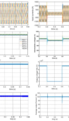
[image:6.595.178.455.45.529.2](12) Fig. 3 MATLAB simulations of AC/DC ISIPOS system
(a) Normal operation, (b) With 80% sudden drop in terminal voltage
From (12), a perturbation increase in the duty ratio of module k leads to a decrease in its input voltage in relation to the other rectifier input voltages. As depicted in Fig. 4c, the duty ratio of Rec_a1 is composed of two parts, namely δ and δsh_a1. δ is common for all phase a rectifiers and generated from the overall central controller while δsh_a1 is generated from the ISOS sharing
controller for Rec_a1.
In this research, IVS can be achieved using the decentralised droop controllers shown in Fig. 4c. Unlike the previous IPOS sharing technique, the ISOS technique has positive feedback at summing point 1 (Fig. 4c) in order to give the positive droop regulation characteristics as shown in Fig. 4d. The IVS PI controller Gsh_ac(s) can be expressed as
Gsh_ac(s) = Kp_sh2+ Ki_sh2
s (13)
The transfer function of the closed-loop system Hsh1(s) can be deduced from
g21(s) = v~m_a1
v~ar_a1=1 + GGsh_acsh_ac(s)ggrecrec(s)(s) (14.1)
grec(s) = v~m_a1
δ~sh_a1=
G14(s) G14(s) ⋅ (1 + CacLacs2) + L
acs (14.2)
V~ar_a1= V~pref_a1+ Kev~in_a1 (14.3)
Hsh(s) = v~m_a1
v~pref_a1= 1 − Kegg21(s)g21(s) rec(s) (14.4)
The same approach as that for the IPOS sharing technique with the analysis shown in Fig. 5 was followed, and the controller gains are selected as Kp_sh2 = 5, Ki_sh2 = 120 and Ke = 750 to provide
relatively stable operation and a bandwidth equal to seven times that of the overall AC controller. The presented sharing methods are decoupled from the power transfer process and they do not require communication between the different modules and rectifiers. The system modularity and flexibility are therefore improved. The regulation features of the sharing controllers are not affected by the variation of input and output voltages or currents. The sharing controllers can achieve IVS and ICS of the AC/DC rectifiers and DC/DC modules during transients and under steady-state conditions.
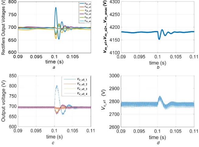
Figs. 6a and b show the MATLAB simulations of the sharing technique for one IPOS group consisting of four of the DC/DC DAB converters shown in Fig. 4a.
At t = 0.1 s, a perturbation occurs and output voltage vo1
increases. It can be seen that the total output voltage was not significantly affected and the controller succeeded in restoring normal operation. Figs. 6c and d show the MATLAB simulations of the sharing techniques for one ISOS group consisting of four DC/AC rectifiers. At t = 0.1 s, a perturbation occurs and output voltage vm1 increases. The controller is able to share the output
[image:7.595.61.281.681.769.2]voltage between the different rectifiers equally. Fig. 4 Converters and rectifier power sharing
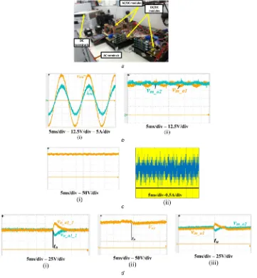
4 Experimental results
A 1 kW prototype controlled with TMS320F28335DSP was built, as shown in Fig. 7a, to validate the presented concept, mathematical analysis and control schemes. The system parameters in this case are shown in Table 4. FGY75N60SMD IGBTs have been employed for the semiconductor switches while RURG3060 diodes have been used for the anti-parallel diodes. During the normal operation shown in Figs. 7b and c, power is transferred
from the input AC side to the output DC side through the ISIPOS system. Fig. 7b(i) shows that phase a current iina is in phase with the input AC voltage vina. However, the power factor is controlled
[image:8.595.113.496.48.360.2]over the full range according to the operation. Fig. 7b(ii) shows the output voltages of the rectifiers. As shown, these voltages have oscillating components beside the desired DC components. However, as long as these components are small they will not affect the normal operation of the system as the rectifier voltage Fig. 5 Variation of IPOS DC converter closed-loop poles with controller proportional gain Kp_sh1
(a)Kd = 100, Ki_sh1 = 200, Kp_sh1 = 3,…,100, (b)Kd = 500, Ki_sh1 = 200, Kp_sh1 = 3,…,100, (c)Kd = 500, Ki_sh1 = 200, Kp_sh1 = 3,…,100, (d) open-loop Bode plot at Kd = 500,
Ki_sh1 = 200 and Kp_sh1 = 25
Fig. 6 Simulated output voltage of ISOS and IPOS sharing technique during voltage perturbations
(a) Individual output voltages of one ISOS group, (b) Total output voltage of one ISOS group, (c) Individual output voltages of one IPOS group, (d) Total output voltage of one IPOS group
[image:8.595.140.467.414.656.2]will be converted using the next stage (IPOS groups). Fig. 7c(i) shows the output DC voltage of the system, whereas Fig. 7c(ii) shows the output current. The oscillating component of the output current can be eliminated either by increasing the value of output filter capacitance or by using simple resonant controllers tuned at the oscillation frequency. The efficiency of the total system is 95% in this case. The results can be compared with the MATLAB simulations in Fig. 3. Fig. 7d shows the results when an intended unbalance occurs at time instant ‘tu’ in the first module of the IPOS
DC/DC converter in phase a. In Fig. 7d(i), the output voltages of the DC/DC modules were forced back to the equilibrium operating
point again after a very short duration by the sharing controllers. Fig. 7d(ii) shows that the total output of the DC/DC group of phase ‘a’ has not been significantly affected by the sudden unbalance. Fig. 7d(iii) shows that the output voltages of the ISOS AC/DC rectifiers in phase a have been restored to their desired equal sharing values shortly after the sudden unbalance.
5 Conclusion
[image:9.595.120.481.50.440.2]In this paper, control schemes suitable for a modular ISIPOS AC/DC energy conversion system are presented and analysed. ISIPOS AC/DC converters are considered as promising solutions for medium-voltage high-power wind energy applications. However, because of their modularity, they can be extended to other applications, such as high-voltage high-power applications. Unfortunately, because the ISIPOS energy conversion system consists of many stages, control design becomes complicated and not straight forward. In this research, the control scheme comprises two main parts, namely, overall control and module-level control. In the overall AC/DC converter control, the series connected AC/DC rectifiers of the input–parallel output-series connected modules are viewed as equivalent AC/DC and DC/DC modules, and the mismatches between the system parameters are neglected. The duty ratios of the different modules are fed from central controllers. In the module-level controllers, each module has its own controller to cater for small mismatches between the different parameters, and to ensure equal voltage and current sharing between the power converters. System-level MATLAB simulations have been conducted to show the effectiveness of the proposed controller design. In addition, scaled-down experiments verify the Fig. 7 Experimental results
[image:9.595.44.287.492.645.2](a) Experimental setup, (b) (i) input current with input voltage and (ii) rectifiers output voltages, (c) (i) total output voltage from phase a and (ii) sampled output current from the controller, (d) (i) and (ii) IPOS sharing technique and (iii) ISOS sharing technique
Table 4 Circuit conditions of experimental setup
Parameter Value
nac and ndc 2
switching frequency fs 50 kHz DAB inductance value L 30 µH transformer turns ratio n 1
Lac and Cac 1 mH and 45 µF
Cdc1 and Cdc2 20 µF
vin and iin 50 V and 10 A (peak)
Kp1 and Ki1 0.25 and 10
Kp2 and Ki2 1 and 8
Kp_sh1, Ki_sh1 and Kd 10, 80 and 200
presented mathematical analysis and simulation results using a 1 kW prototype controlled with TMS320F280335 digital signal processor.
6 Acknowledgments
This work was supported by the Engineering and Physical Sciences Research Council (EPSRC) under grant EP/K035096/1.
7 References
[1] EWEA Association.: ‘Wind in power 2015 statistics’, Available at: http:// www.ewea.org/fileadmin/files/library/publications/statistics/EWEAAnnual-Statistics-2015.pdf
[2] Wu, B., Wu, L., Zargari, N., et al.: ‘Power conversion and control of wind energy systems’ (Wiley, 2011)
[3] Barrenetxea, M., Baraia, I., Adam, G.P., et al.: ‘Analysis, comparison and selection of DC–DC converters for a novel modular energy conversion scheme for DC offshore wind farms’. EUROCON, 2015
[4] ABB: ‘HVDC Light® It's time to connect’, Available at: https:// library.e.abb.com/public/2742b98db321b5bfc1257b26003e7835/
Pow0038%20R7%20LR.pdf
[5] Zubiaga, M., Abad, G., Barrena, J.A., et al.: ‘Energy transmission and grid integration of AC offshore wind farms InTech’, 2012
[6] Holtsmark, N., Bahirat, H., Molinas, M., et al.: ‘An all DC offshore wind farm with series-connected turbines: an alternative to the classical parallel AC model?’, IEEE Trans. Ind. Electron., 2013, 60, (6), pp. 2420–2428 [7] Barrenetxea, M., Baraia, I., Larrazabal, I., et al.: ‘Design of a novel modular
energy conversion scheme for DC offshore wind farms’. IEEE EUROCON – Int. Conf. on Computer as a Tool 2015, 2015
[8] Pan, J., Bala, S., Callavik, M., et al.: ‘DC connection of offshore wind power plants without platform’. Presented at the 13th Wind Integration Workshop, Berlin, 2014
[9] Yiqing, L., Finney, S.J.: ‘DC collection networks for offshore generation’. Renewable Power Generation Conf. (RPG 2013), 2nd IET, Beijing, 2013 [10] Stieneker, M., Riedel, J., Soltau, N., et al.: ‘Design of series-connected
dual-active bridges for integration of wind park cluster into MVDC grids’, EPE'14-ECCE Europe, Lappeenranta, 2014
[11] Adam, G.P., Williams, B.W.: ‘Half- and full-bridge modular multilevel converter models for simulations of full-scale HVDC links and multiterminal DC grids’, IEEE J. Emerg. Sel. Top. Power Electron., 2014, 2, (4), pp. 1089– 1108
[12] Lian, Y., Adam, G.P., Holliday, D., et al.: ‘Medium-voltage DC/DC converter for offshore wind collection grid’, IET Renew. Power Gener., 2016, 10, (5), pp. 651–660
[13] Chen, W., Huang, A.Q., Li, C., et al.: ‘Analysis and comparison of medium voltage high power DC/DC converters for offshore wind energy systems’,
IEEE Trans. Power Electron., 2013, 28, pp. 2014–2023
[14] Aboushady, A.A.: ‘Design, analysis and modelling of modular medium-voltage DC/DC converter based systems’. PhD thesis, University of Strathclyde, Glasgow, 2012
[15] Wong, S.C., Brown, A.D.: ‘Analysis, modeling and simulation of series-parallel resonant converter circuits’, IEEE Trans. Power Electron., 1995, 10, (5), pp. 605–614
[16] Agamy, M.S., Jain, P.K.: ‘A variable frequency phase-shift modulated three-level resonant single-stage power factor correction converter’, IEEE Trans. Power Electron., 2008, 23, (5), pp. 2290–2300
[17] Chen, H., Sng, E.K., Tseng, K.J.: ‘Generalized optimal trajectory control for closed loop control of series-parallel resonant converter’, IEEE Trans. Power Electron., 2006, 21, (5), pp. 1347–1355
[18] Sano, K., Fujita, H.: ‘Performance of high-efficiency switchedcapacitor-based resonant converter with phase-shift control’, IEEE Trans. Power Electron., 2011, 26, (2), pp. 344–354
[19] Bhat, A.: ‘Fixed-frequency PWM series-parallel resonant converter’, IEEE Trans. Ind. Appl., 1992, 28, (5), pp. 1002–1009
[20] Zhao, B., Song, Q., Liu, W., et al.: ‘Overview of dual-active-bridge isolated bidirectional DC–DC converter for high-frequency-link power-conversion system’, IEEE Trans. Power Electron., 2014, 29, (8), pp. 4091–4106 [21] Giri, R., Choudhary, V., Ayyanar, R., et al.: ‘Common-duty-ratio control of
input-series connected modular dc–dc converters with active input voltage and load-current sharing’, IEEE Trans. Ind. Appl., 2006, 42, (4), pp. 1101– 1111
[22] Chen, W., Ruan, X., Yan, H., et al.: ‘DC/DC conversion system consisting of multiple converter modules: stability, control, and experimental verifications’,
IEEE Trans. Power Electron., 2009, 24, (6), pp. 1463–1474
[23] Chen, W., Wang, G.: ‘Decentralized voltage-sharing control strategy for fully modular input-series–output-series system with improved voltage regulation’,
IEEE Trans. Ind. Electron., 2015, 62, (5), pp. 2777–2787
[24] Mease, K.D., Topcu, U.: ‘Two-timescale nonlinear dynamics and slow manifold determination’. Presented at the AIAA Guidance, Navigation, and Control Conf. and Exhibit, San Francisco, CA, August 2005, AIAA, pp. 2005–5846
[25] Bacha, S., Munteanu, I., Bratcu, A.I.: ‘Power electronic converters modeling and control: with case studies’ (Springer, 2014)
[26] Darwish, A., Massoud, A., Holliday, D., et al.: ‘Single-stage three-phase differential-mode buck-boost inverters with continuous input current for PV applications’, IEEE Trans. Power Electron., 2016, 31, (12), pp. 8218–8236
8 Appendix
8.1 Average model of bidirectional DAB
Operation when the DAB is controlled with PSC can be explained as shown in Fig. 8b. The state-space representation can be arranged as
i I: 0 < t ≤ Dts
dV1 dt diL dt dV2 dt = −1
r1C1 −1C1 0
1
L 0 nL1
0 nC−1 2
−1
r2C2
V1
iL V2
+ 1
r1C1 0
0 0
0 r1 2C2
Vdc1 Vdc2
(15)
ii II: Dts < t ≤ (1−D)ts
dV1 dt diL dt dV2 dt = −1
r1C1 −1C1 0
1
L 0 −1nL
0 nC1 2
−1
r2C2
V1
iL V2
+ 1
r1C1 0
0 0
0 r1 2C2
Vdc1 Vdc2
(16)
Operation in durations (I and II) is symmetrical to that during (III and IV), so durations I and II will be considered.
It can be noted that two states, namely V1 and V2, are varying
much more slowly than the third variable iL. So, the system under
investigation is a two-time scale system [24].
Equating (diL/dt) to zero and substituting for iL in (dV1/dt) and (dV2/dt), the equations yield
dV1
dt =r11C1Vdc1− 1r1C1V1− 1C1iL dV2
dt =r21C2Vdc2− 1r2C2V1− 1nC2iL
iL=V1+ V2/n
L t + 12 fsL[(1 − 2D) − nV1])
0 < t ≤ Dts (17)
where
dV1
dt =r11C1Vdc1− 1r1C1V1− 1C1iL dV2
dt =r21C2Vdc2− 1r2C2V1+ 1nC2iL
iL=V1− V2/n
L (t − Dts) + 12 f
sL[V2− n(1 − 2D)V1]) Dts
< t ≤ ts
(18)
Arranging and averaging over the period ts gives
dV¯ 1 dt dV¯ 2 dt
= −1
r1C1 D
2− D
L fsC1 D − D2
L fsC2 r−12C2 V¯
1
V¯ 2
+ 1
r1C1 0
0 r1 2C2
Vdc1 Vdc2 (19)
8.2 DAB converter small-signal model
The equations in (19) can be written as
dV1
dt =r−11C1V1+ D 2− D
L fsC1V2+ 1r1C1Vdc1
f1
dV2
dt =D − D 2
L fsC2V1+ −1r
2C2V2+ 1r2C2Vdc2
f2
(20)
The small-signal model can be expressed as [25, 26]
dv~1 dt dv~2
dt =
∂ f1 ∂V1
∂ f1 ∂V2 ∂ f2 ∂V1
∂ f2 ∂V2
v~1 v~2
+ ∂ f1 ∂Vdc1
∂ f1 ∂Vdc2
∂ f1 ∂d ∂ f2
∂Vdc1 ∂ f2 ∂Vdc2
∂ f2 ∂d
v~dc1 v~dc2 d
(21)
Hence
dv~1 dt dv~2
dt =
−1
r1C1 D
2− D
L fsC1 D − D2
L fsC2 r−12C2 v~1 v~1
+ 1
r1C1 0 2D − 1L fsC1V2
0 r1 2C2
1 − 2D
L fsC2V1
v~dc1 v~dc2 d
[image:11.595.122.479.51.409.2](22) Fig. 8 DAB and AC/DC rectifiers
Therefore, the small-signal transfer functions of the system can be expressed as (see (23a))
(see (23b)) (see (23c)) (see (23d)) (see (24a)) (see (24b)) (see (24c))
8.3 Bidirectional AC/DC converter average model
The state-space representation of the circuit can be expressed as
diin dt dVco
dt =
0 −1L
in
1
Co 0 iin Vco +
1
Lin 0
0 −1C
o vin
Io (25)
δ: iin decreases and Vco increases (25)
diin dt dVco
dt
= 0 00 0 Viin
co +
1
Lin 0
0 −1C
o vin
Io (26)
1−δ: iin increases and Vco decreases (26).
Similarly, the average equations of the AC/DC rectifier can be written as
v~co= 1 + Cδ~
oLins2Vin− Lins
1 + CoLins2i~o (27)
Equation (27) can be rewritten as
v~co= 1 + Cδ~
oLins2Vin− Lins
1 + CoLins2
v~co
G14 (28)
Rearranging (28)
G11(s) = v~1
v~dc1
= L2fs2(sC2r2+ 1) (C1C2L2f
s
2r1r2)s2+ L2f
s
2(C1r1+ C2r2)s +r1D2(r2D2− 2r2D +r2) + L2f
s
2)
(23a)
G12(s) = v~1
v~dc2
= DLfsr1(D − 1)
(C1C2L2f
s
2r1r2)s2+ L2f
s
2(C1r1+ C2r2)s +r1D2(r2D2− 2r2D +r2) + L2f
s
2)
(23b)
G13(s) =v~1
d
= LC2Vdc2fsr1r2(2D − 1)s +r1(2D − 1)(V1r2D(1 − D) + LVdc1fs)
(C1C2L2f
s
2r1r2)s2+ L2f
s
2(C1r1+ C2r2)s +r1D2(r2D2− 2r2D +r2) + L2f
s
2)
(23c)
G14(s) = i ~
in v~dc1
= (C1C2L2fs2r2)s2+ L2fs2C1s + D2(r2D2− 2r2D +r2) (C1C2L2f
s
2r1r2)s2+ L2f
s
2(C1r1+ C2r2)s +r1D2(r2D2− 2r2D +r2) + L2f
s
2)
(23d)
G21(s) = v~2
v~dc1
= Lfsr2D(1 − D)
(C1C2L2f
s
2r1r2)s2+ L2f
s
2(C1r1+ C2r2)s +r1D2(r2D2− 2r2D +r2) + L2f
s
2)
(24a)
G22(s) = v~2
v~dc2
= L2fs2(sC1r1+ 1) (C1C2L2f
s
2r1r2)s2+ L2f
s
2(C1r1+ C2r2)s +r1D2(r2D2− 2r2D +r2) + L2f
s
2)
(24b)
G23(s) =v~2
d
= LC1Vdc1fsr1r2(1 − 2D)s − r2(2D − 1)(Vdc2r2D(D − 1)+LVdc2fs)
(C1C2L2f
s
2r1r2)s2+ L2f
s
2(C1r1+ C2r2)s +r1D2(r2D2− 2r2D +r2) + L2f
s
2)
(24c)
Gac(s) =v~δ~oc= G14(1 + CG14
![Fig. 2 (a)Frequency domain analysis of overall DC/DC converters Closed-loop pole-zero map and open-loop Bode plot (Kp1 = 0.5 and Ki1 = [10 : 50]), (b) Closed-loop pole-zero map and open-loop Bode plot (Ki1 = 15 and Kp1 = [0.1:1]), (c)Closed-loop pole-zero map and open-loop Bode plot (Kp2 = 3 and Ki2 = [10:20]), (d) Closed-loop pole-zero map and open-loop Bode plot (Ki2 = 15 and Kp2 = [1:10])](https://thumb-us.123doks.com/thumbv2/123dok_us/1442191.96625/5.595.119.480.47.594/frequency-analysis-overall-converters-closed-closed-closed-closed.webp)